Maynard, MA, June 25, 2025, EFFECT Photonics, a leading provider of next-generation coherent optical solutions for data center and edge networks, today announced it has raised an additional $24 million as part of its Series D financing round. This brings the total raised in the round to $62 million. The new capital underscores the ongoing commitment of existing investors and
Maynard, MA, June 25, 2025, EFFECT Photonics, a leading provider of next-generation coherent optical solutions for data center and edge networks, today announced it has raised an additional $24 million as part of its Series D financing round. This brings the total raised in the round to $62 million.
The new capital underscores the ongoing commitment of existing investors and their continued confidence in EFFECT Photonics’ leadership in coherent technology and growing commercial momentum with leading industry partners
Maynard, MA, June 25, 2025, EFFECT Photonics, a leading provider of next-generation coherent optical solutions for data center and edge networks, today announced it has raised an additional $24 million as part of its Series D financing round. This brings the total raised in the round to $62 million. The new capital underscores the ongoing commitment of existing investors and their continued confidence in EFFECT Photonics’ leadership in coherent technology and growing commercial momentum with leading industry partners “This funding milestone reinforces the strong market demand we’re seeing and allows us to execute aggressively on our roadmap,” said Roberto Marcoccia, CEO of EFFECT Photonics. “We’re grateful for the continued support of our investors and partners as we scale to meet the needs of a rapidly growing optical interconnect market.” The Series D round follows significant technical and commercial progress. The company’s solutions are enabling the next wave of high-performance networking at the edge and AI infrastructure.
Join EFFECT Photonics from April 1 to 3, 2025 at the 50th OFC in San…
Join EFFECT Photonics from April 1 to 3, 2025 at the 50th OFC in San Francisco, California, the world’s largest event for optical networking and communications, to discover firsthand how our technology is transforming where light meets digital. Visit Booth #2850 to learn how EFFECT Photonics’ full portfolio of optical building blocks are enabling 100G coherent to the network edge and next-generation applications.
What to Expect in 2025:
Global Participation: Anticipate over 13,500 participants from 83+ countries, alongside 670 exhibiting companies, making it a truly international affair.
Innovation Hub: Witness the debut of startups and the pioneering strides of industry leaders, setting the tone for the future of optical communications.
Inclusive Programs: Immerse yourself in a diverse array of programs and events designed to encompass the entire ecosystem, with a strong emphasis on inclusivity.
Key Highlights:
Interoperability Demonstrations: Experience live demonstrations by leading optics companies, showcasing seamless integration over OFCnet.
Plenary Sessions: be inspired by industry luminaries as they delve into the transformative power of technology and its impact on our world.
Cloud computing offers scalable and flexible IT resources over the Internet, allowing businesses to avoid…
Cloud computing offers scalable and flexible IT resources over the Internet, allowing businesses to avoid the upfront cost and complexity of owning and maintaining their own IT infrastructure. Cloud services allow organizations to access a wide array of computing resources on demand, such as servers, storage, databases, and software applications.
Edge computing complements cloud computing by processing data near the source rather than relying on a central data center. This is important for applications requiring real-time processing and low latency, such as autonomous vehicles, industrial automation, and smart city technologies. By minimizing the distance data must travel, edge computing reduces latency, increases data processing speed, and could also increase data privacy and reliability.
These advantages are causing the global market for edge computing to explode, with STL Partners predicting that the total edge computing addressable market will grow from $9 billion in 2020 to $445 billion in 2030. They also forecast that the number of edge data center sites will triple, from 491 in 2023 to 1584 in 2025.
Various trends are driving the rise of the edge cloud:
5G technology and the Internet of Things (IoT): These mobile networks and sensor networks need low-cost computing resources closer to the user to reduce latency and better manage the higher density of connections and data.
Content delivery networks (CDNs): The popularity of CDN services continues to grow, and most web traffic today is served through CDNs, especially for major sites like Facebook, Netflix, and Amazon. By using content delivery servers that are more geographically distributed and closer to the edge and the end user, websites can reduce latency, load times, and bandwidth costs as well as increasing content availability and redundancy.
Software-defined networks (SDN) and Network function virtualization (NFV). The increased use of SDNs and NFV requires more cloud software processing.
Augment and virtual reality applications (AR/VR): Edge data centers can reduce the streaming latency and improve the performance of AR/VR applications.
However, in this article, we will discuss arguably the most important trend powering the explosive growth of the edge data center sector: artificial intelligence.
The Impact of AI on Edge Data Centers
AI will enhance many of the applications we mentioned before, including real-time analytics, autonomous vehicles, augmented reality, and IoT devices, which require low-latency data processing and immediate decision-making capabilities.
As AI workloads grow, traditional centralized data centers face challenges in handling the sheer volume of data generated at the edge. Due to these challenges, there is increased motivation to move these AI workloads towards the network edge. Edge data centers provide a decentralized solution, distributing computing resources closer to end-users and devices, which reduces the strain on centralized cloud infrastructures.
This proximity to the end user allows for more real-time data processing and decision-making, which is critical for applications that require immediate responses. Industries such as manufacturing, healthcare, retail, and smart cities could benefit from edge AI. For instance, in manufacturing, edge AI can monitor machinery in real-time to predict and prevent failures, enhancing operational efficiency and reducing downtime. In healthcare, edge AI enables real-time patient monitoring, providing immediate alerts to medical staff about critical changes in patient conditions.
The integration of AI at the edge also addresses the growing need for data privacy and security. By processing data locally, sensitive information does not need to be transmitted to centralized cloud servers, reducing the size and risk of data breaches and streamlining compliance with data protection regulations. Moreover, edge AI reduces the bandwidth required for data transfer, as only the necessary information is sent to the cloud, optimizing network resources and reducing costs.
The Value of Edge Data Centers
Several of these applications require lower latencies than before, and centralized cloud computing cannot deliver those data packets quickly enough. As shown in Table 1, a data center on a town or suburb aggregation point could halve the latency compared to a centralized hyperscale data center. Enterprises with their own data center on-premises can reduce latencies by 12 to 30 times compared to hyperscale data centers.
Types of Edge Data Centres
Types of Edge
Data center
Location
Number of DCs per 10M people
Average Latency
Size
On-premises edge
Enterprise site
Businesses
NA
2-5 ms
1 rack max
Network (Mobile)
Tower edge
Tower
Nationwide
3000
10 ms
2 racks max
Outer edge
Aggregation points
Town
150
30 ms
2-6 racks
Inner edge
Core
Major city
10
40 ms
10+ racks
Regional edge
Regional edge
Regional
Major city
100
50 ms
100+ racks
Not edge
Not edge
Hyperscale
State/national
1
60+ ms
5000+ racks
Types of edge data centers and their characteristics. Source: STL Partners
Cisco estimates that 85 zettabytes of useful raw data were created in 2021, but only 21 zettabytes were stored and processed in data centers. Edge data centers can help close this gap. For example, industries or cities can use edge data centers to aggregate all the data from their sensors. Instead of sending all this raw sensor data to the core cloud, the edge cloud can process it locally and turn it into a handful of performance indicators. The edge cloud can then relay these indicators to the core, which requires a much lower bandwidth than sending the raw data.
Distributing data centers is also vital for future data center architectures. While centralizing processing in hyper-scale data centers made them more energy-efficient, the power grid often limits the potential location of new hyperscale data centers. Thus, the industry may have to take a few steps back and decentralize data processing capacity to cope with the strain of data center clusters on power grids. For example, data centers can be relocated to areas where spare power capacity is available, preferably from nearby renewable energy sources. EFFECT Photonics envisions a system of datacentres with branches in different geographical areas, where data storage and processing are assigned based on local and temporal availability of renewable (wind-, solar-) energy and total energy demand in the area.
Figure 1: High-speed fiber-optic connections allow data processing and storage to move to locations where excess (green) energy is available. If power is needed for other purposes, such as charging electric vehicles, data can be moved elsewhere
Coherent Technology Simplifies the Scaling of Edge Interconnects
As edge data center interconnects became more common, the issue of how to interconnect them became more prominent. Direct detect technology had been the standard in the short-reach data center interconnects. However, reaching the distances greater than 50km and bandwidths over 100Gbps required for modern edge data center interconnects required external amplifiers and dispersion compensators that increased the complexity of network operations.
At the same time, advances in electronic and photonic integration allowed longer reach coherent technology to be miniaturized into QSFP-DD and OSFP form factors. This progress allowed the Optical Internetworking Forum (OIF) to create the 400ZR and ZR+ standards for 400G DWDM pluggable modules. With small enough modules to pack a router faceplate densely, the datacom sector could profit from a 400ZR solution for high-capacity data center interconnects of up to 80km. If needed, extended reach 400ZR+ pluggables can cover several hundreds of kilometers. Cignal AI forecasts that 400ZR shipments will dominate in the edge applications, as shown in Figure 3.
Figure 3: Forecast of 100G port equivalents shipped for edge applications. These shipments are overwhelmingly 400ZR standard technology. Source: Cignal AI Transport Applications Report Q42021.
Further improvements in integration can further boost the reach and efficiency of coherent transceivers. For example, by integrating all photonic functions on a single chip, including lasers and optical amplifiers, EFFECT Photonics’ optical System-On-Chip (SoC) technology can achieve higher transmit power levels and longer distances while keeping the smaller QSFP-DD form factor, power consumption, and cost.
Takeaways
Edge computing is becoming increasingly critical for supporting AI-driven applications, such as autonomous vehicles, real-time analytics, and smart city technologies. The proximity of edge data centers to end-users allows for faster data processing, lower latency, and improved data privacy. This shift is driven by the growing need for real-time decision-making capabilities and compliance with data protection regulations. As AI workloads continue to expand, edge data centers provide a decentralized solution that alleviates the pressure on centralized cloud infrastructures and optimizes network resources.
(First published on the 2nd November 2022 updated 4th September 2024) Thanks to wafer-scale technology,…
(First published on the 2nd November 2022 updated 4th September 2024)
Thanks to wafer-scale technology, electronics have driven down the cost per transistor for many decades. This allowed the world to enjoy chips that every generation became smaller and provided exponentially more computing power for the same amount of money. This scale-up process is how everyone now has a computer processor in their pocket that is millions of times more powerful than the most advanced computers of the 1960s that landed men on the moon.
This progress in electronics integration is a key factor that brought down the size and cost of coherent transceivers, packing more bits than ever into smaller areas. However, photonics has struggled to keep up with electronics, with the photonic components dominating the cost of transceivers. If the transceiver cost curve does not continue to decrease, it will be challenging to achieve the goal of making them more accessible across the entire optical network.
To trigger a revolution in the use of photonics worldwide, it needs to be as easy to use as electronics. In the words of our Chief Technology Officer, Tim Koene-Ong:
“We need to buy photonics products from a catalog as we do with electronics, have datasheets that work consistently, be able to solder it to a board and integrate it easily with the rest of the product design flow.”
Tim Koene-Ong, Chief Technology Officer.
This goal requires photonics manufacturing to leverage existing electronics manufacturing processes and ecosystems. Photonics must embrace fabless models, chips that can survive soldering steps, and electronic packaging and assembly methods.
The Advantages of a Fabless Model
Increasing the volume of photonics manufacturing is a big challenge. Some photonic chip developers manufacture their chips in-house within their fabrication facilities. This approach has substantial advantages, giving component manufacturers complete control over their production process.
Figure 1: Simplified value chain diagram of a vertically-integrated optical transceiver developer. The developer handles the PIC design, manufacturing, and packaging.
However, this approach has its trade-offs when scaling up. If a vertically integrated chip developer wants to scale up in volume, they must make a hefty capital expenditure (CAPEX) in more equipment and personnel. They must develop new fabrication processes as well as develop and train personnel. Fabs are not only expensive to build but to operate. Unless they can be kept at nearly full utilization, operating expenses (OPEX) also drain the facility owners’ finances.
Especially in the case of an optical transceiver market that is not as big as that of consumer electronics, it’s hard not to wonder whether that initial investment is cost-effective. For example, LightCounting research data estimates that 173 million optical Ethernet transceivers were sold in 2023, while the International Data Corporation estimates that 1.17 billion smartphones were sold in 2023. The latter figure is seven times larger than the entire optical transceiver market.
Electronics manufacturing experienced a similar problem during their 70s and 80s boom, with smaller chip start-ups facing almost insurmountable barriers to market entry because of the massive CAPEX required. Furthermore, the large-scale electronics manufacturing foundries had excess production capacity that drained their OPEX. The large-scale foundries sold that excess capacity to the smaller chip developers, who became fabless. In this scenario, everyone ended up winning. The foundries serviced multiple companies and could run their facilities at total capacity, while the fabless companies could outsource manufacturing and reduce their expenditures.
This fabless model, with companies designing and selling the chips but outsourcing the manufacturing, should also be the way for photonics. Instead of going through a more costly, time-consuming process, the troubles of scaling up for photonics developers are outsourced and (from the perspective of the fabless company) become as simple as putting a purchase order in place. Furthermore, the fabless model allows photonics developers to concentrate their R&D resources on the end market. This is the simplest way forward if photonics moves into million-scale volumes.
Adopting Electronics-Style Packaging
While packaging, assembly, and testing are only a small part of the cost of electronic systems, the reverse happens with photonic integrated circuits (PICs). Researchers at the Technical University of Eindhoven (TU/e) estimate that for most Indium Phosphide (InP) photonics devices, the cost of packaging, assembly, and testing can reach around 80% of the total module cost.
Figure 2 . Process cost breakdown of an InP PIC-based module as a percentage of the overall manufacturing cost. Source: Latkowski et al., 2019
To become more accessible and affordable, the photonics manufacturing chain must become more automated and standardized. The lack of automation makes manufacturing slower and prevents data collection that can be used for process control, optimization, and standardization.
One of the best ways to reach these automation and standardization goals is to learn from electronics packaging, assembly, and testing methods that are already well-known and standardized. After all, building a special production line is much more expensive than modifying an existing production flow.
There are several ways in which photonics packaging, assembly, and testing can be made more affordable and accessible. Below are a few examples:
Passive alignments: Connecting optical fiber to PICs is one of optical devices’ most complicated packaging and assembly problems. The best alignments are usually achieved via active alignment processes in which feedback from the PIC is used to align the fiber better. Passive alignment processes do not use such feedback. They cannot achieve the best possible alignment but are much more affordable.
BGA-style packaging: Ball-grid array packaging has grown popular among electronics manufacturers. It places the chip connections under the chip package, allowing more efficient use of space in circuit boards, a smaller package size, and better soldering.
Figure 3: Top, bottom, and side views of a ball-grid array (BGA) style package.
Flip-chip bonding: A process where solder bumps are deposited on the chip in the final fabrication step. The chip is flipped over and aligned with a circuit board for easier soldering.
Figure 4: Simplified steps of the flip chip bonding process.
These might be novel technologies for photonics developers who have started implementing them in the last five or ten years. However, the electronics industry embraced these technologies 20 or 30 years ago. Making these techniques more widespread will make a massive difference in photonics’ ability to scale up and become as available as electronics.
Making Photonics Chips That Can Survive Soldering
Soldering remains another tricky step for photonics assembly and packaging. Photonics device developers usually custom order a PIC, then wire and die bond to the electronics. However, some elements in the PIC cannot handle soldering temperatures, making it difficult to solder into an electronics board. Developers often must glue the chip onto the board with a non-standard process that needs additional verification for reliability.
This goes back to the issue of process standardization. Current PICs often use different materials and processes from electronics, such as optical fiber connections and metals for chip interconnects, that cannot survive a standard soldering process.
Adopting BGA-style packaging and flip-chip bonding techniques will make it easier for PICs to survive this soldering process. There is ongoing research and development worldwide, including at EFFECT Photonics, to make fiber coupling and other PIC aspects compatible with these electronic packaging methods.
PICs that can handle being soldered to circuit boards will allow the industry to build optical subassemblies that can be made more readily available in the open market and can go into trains, cars, or airplanes.
Conclusion
Photonics must leverage existing electronics ecosystems and processes to scale up and have a greater global impact. Our Chief Technology Officer, Tim Koene-Ong, explains what this means:
Photonics technology needs to integrate more electronic functionalities into the same package. It needs to build photonic integration and packaging support that plays by the rules of existing electronic manufacturing ecosystems. It needs to be built on a semiconductor manufacturing process that can produce millions of chips in a month.
As soon as photonics can achieve these larger production volumes, it can reach price points and improvements in quality and yield closer to those of electronics. When we show the market that photonics can be as easy to use as electronics, that will trigger a revolution in its worldwide use.
Our Chief Technology Officer, Tim Koene-Ong.
This vision is one of our guiding lights at EFFECT Photonics, where we aim to develop optical systems that can impact the world in many different applications.
The Internet of Things (IoT) is transforming industries by enabling devices to communicate, collect, and…
The Internet of Things (IoT) is transforming industries by enabling devices to communicate, collect, and exchange data seamlessly. This interconnected ecosystem relies on robust, high-speed communication technologies to function effectively. Photonics, which involves the use of light to transmit data, plays a critical role in enhancing the connectivity of IoT devices. This article explores the different ways photonics enables IoT, focusing on high-speed data transmission, energy-efficient sensing, and the development of smart, self-powered devices.
High-Speed Data Transmission
The advent of 5G technology, with its promise of ultra-fast speeds and low latency, has enabled many IoT applications, turning mundane devices into smart, interconnected components of broader digital ecosystems. However, this means more devices contribute to the already vast data streams flowing through global networks.
Figure 1: tower with 5G cellular network antenna on city background
Photonics significantly enhances data transmission speeds in IoT networks, making it possible to handle the massive data volumes generated by connected devices. Optical fibers, which use light to transmit data, offer higher bandwidth and lower latency compared to traditional copper wires. This is essential for applications that require real-time data processing and rapid communication, such as autonomous vehicles, smart grids, and industrial automation.
Energy-Efficient Sensing
Photonics also plays a vital role in the development of energy-efficient sensing technologies for IoT. Photonic sensors offer high sensitivity and accuracy with much low power consumption. This is particularly important for applications in remote or hard-to-reach locations where replacing batteries is impractical.
Photonic integrated circuits (PICs) combine multiple optical components on a single chip, enabling faster and more efficient data transmission. For instance, advances in PIC technology have enabled high-performance LiDAR systems, which use laser pulses to create detailed 3D maps of environments. These systems are crucial for applications like autonomous driving, where precise and real-time data is necessary.
Figure 2: Visualization of the interaction of self-driving autonomous vehicles. Robotic cars are controlled by AI, driving along a busy city avenue, scanning the road with sensors, and exchanging information.
Smart, Self-Powered Devices
One of the most exciting developments in photonics for IoT is the creation of self-powered devices. These devices use ambient light to generate the energy needed for their operation, eliminating the need for batteries. This not only reduces maintenance costs but also minimizes environmental impact by decreasing the number of disposable batteries used.
For example, Ambient Photonics is a company that specializes in developing and manufacturing low-light energy harvesting solar cells. The company’s solar cells are thin, efficient, and capable of capturing energy from a wide range of light conditions, including dim indoor settings where traditional solar cells are less effective. Their technology is designed to generate power from low-light environments, such as indoor lighting, which can be used to power various electronic devices without the need for batteries or frequent recharging. This makes them suitable for powering IoT devices, remote sensors, and other small electronics that are often used indoors.
Conclusion
Photonics is enabling the connectivity and functionality of IoT networks. By enabling high-speed data transmission, energy-efficient sensing, and the development of smart, self-powered devices, photonics addresses many of the challenges faced by traditional electronic technologies.
Artificial Intelligence (AI) networks rely on vast amounts of data processed and transferred at incredible…
Artificial Intelligence (AI) networks rely on vast amounts of data processed and transferred at incredible speeds to function effectively. This data-intensive nature requires robust infrastructure, with lasers playing a pivotal role. AI networks depend on two primary processes: AI training and AI inference. Training involves feeding large datasets into models to learn and make predictions, while inference uses these trained models to make real-time decisions.
Lasers are crucial in enhancing the efficiency and speed of these processes by enabling high-speed data transfer within data centers and across networks. This article explores the various ways lasers power AI networks, the specific requirements for data center connections, and their broader impact on AI infrastructure.
Requirements for Data Center Connections
The connectivity requirements for data centers supporting AI workloads are stringent. They must handle enormous volumes of data with minimal latency and high reliability. The primary requirements for lasers in these environments include:
High Bandwidth: AI applications, especially those involving large language models and real-time data processing, require interconnects that can support high data rates.
Low Latency: Minimizing latency is crucial for AI inference tasks that require real-time decision-making. Lasers enable faster data transfer compared to traditional electronic interconnects, significantly reducing the time it takes for data to travel between nodes.
Energy Efficiency: AI data centers consume vast amounts of power. Integrated photonics combines optical components on a single chip, reducing power consumption while maintaining high performance.
Scalability: As AI workloads grow, the infrastructure must scale accordingly. Lasers provide the scalability needed to expand data center capabilities without compromising performance.
Lasers Arrays in Data Center Interconnects
In 2022, Intel Labs demonstrated an eight-wavelength laser array fully integrated on a silicon wafer. These milestones are essential for optical transceivers because the laser arrays can allow for multi-channel transceivers that are more cost-effective when scaling up to higher speeds.
Let’s say we need an intra-DCI link with 1.6 Terabits/s of capacity. There are three ways we could implement it:
Four modules of 400G: This solution uses existing off-the-shelf modules but has the largest footprint. It requires four slots in the router faceplate and an external multiplexer to merge these into a single 1.6T channel.
One module of 1.6T: This solution will not require the external multiplexer and occupies just one plug slot on the router faceplate. However, making a single-channel 1.6T device has the highest complexity and cost.
One module with four internal channels of 400G: A module with an array of four lasers (and thus four different 400G channels) will only require one plug slot on the faceplate while avoiding the complexity and cost of the single-channel 1.6T approach.
Table 1: Comparison of different ways to implement a 1.6 Terabit/s link: four modules of 400G, a single-channel 1.6T module, and a module with four channels of 400G.
Multi-laser array and multi-channel solutions will become increasingly necessary to increase link capacity in coherent systems. They will not need more slots in the router faceplate while simultaneously avoiding the higher cost and complexity of increasing the speed with just a single channel.
Broader Impact on AI Infrastructure
Beyond data centers, lasers are transforming the broader AI infrastructure by enabling advanced applications and enhancing network efficiency. In the context of edge computing, where data is processed closer to the source, lasers facilitate rapid data transfer and low-latency processing. This is essential for applications like autonomous vehicles, smart cities, and real-time analytics, where immediate data processing is critical.
Lasers also play a significant role in the integration of AI with 5G and future 6G networks. The high-frequency demands of these networks require precise and high-speed optical interconnects, which lasers provide.
Conclusion
Lasers are at the core of modern AI networks, providing the high-speed, low-latency, and energy-efficient interconnects needed to support data-intensive AI workloads. From enhancing data center connectivity to enabling advanced edge computing and network integration, lasers play a pivotal role in powering AI. As AI continues to evolve and expand into new applications, the reliance on laser technology will only grow, driving further innovation and efficiency in AI infrastructure.
Artificial Intelligence (AI) can impact several different industries by enhancing efficiency, automation, and data processing…
Artificial Intelligence (AI) can impact several different industries by enhancing efficiency, automation, and data processing capabilities. The network edge is another area where AI can deliver such improvements. Edge computing, combined with AI, enables data processing closer to the source of data generation, leading to reduced latency, improved real-time data analytics, and enhanced security. This article delves into the potential of AI at the network edge, exploring its applications, training and inference processes, and future impact.
The Potential of AI at the Network Edge
According to market research, the global market for edge computing technologies is projected to grow from $46.3 billion in 2022 to $124.7 billion by 2027.
AI at the network edge involves deploying AI models and algorithms closer to where data is generated, such as in IoT devices, sensors, and local servers. This proximity allows for real-time data processing and decision-making, which is critical for applications that require immediate responses. Industries such as manufacturing, healthcare, retail, and smart cities are prime beneficiaries of edge AI. For instance, in manufacturing, edge AI can monitor machinery in real-time to predict and prevent failures, enhancing operational efficiency and reducing downtime. In healthcare, edge AI enables real-time patient monitoring, providing immediate alerts to medical staff about critical changes in patient conditions.
Figure 1: Robotic vision sensor camera system in a smart PCB factory.
The integration of AI at the edge also addresses the growing need for data privacy and security. By processing data locally, sensitive information does not need to be transmitted to centralized cloud servers, reducing the risk of data breaches and ensuring compliance with data protection regulations. Moreover, edge AI reduces the bandwidth required for data transfer, as only the necessary information is sent to the cloud, optimizing network resources and reducing costs.
Training and Inference at the Edge
Training AI models involves feeding large datasets into algorithms to enable them to learn patterns and make predictions. Traditionally, this process requires significant computational power and is often performed in centralized data centers. However, advancements in edge computing and model optimization techniques have made it possible to train AI models at the edge.
One of the key techniques for enabling AI training at the edge is model optimization. This includes methods such as pruning, quantization, and low-rank adaptation, which reduce the size and complexity of AI models without compromising their performance. Pruning involves removing less important neurons or layers from a neural network, while quantization reduces the precision of the model’s weights, making it more efficient in terms of memory and computational requirements. Low-rank adaptation focuses on modifying only a subset of parameters, which is particularly useful for fine-tuning pre-trained models on specific tasks.
Inference, the process of making predictions using a trained AI model, is especially critical at the edge. It requires lower computational power compared to training and can be optimized for low-latency and energy-efficient operations. Edge devices equipped with AI inference capabilities can analyze data in real-time and provide immediate feedback. For example, in retail, edge AI can facilitate frictionless checkout experiences by instantly recognizing and processing items, while in smart cities, it can manage traffic and enhance public safety by analyzing real-time data from surveillance cameras and sensors.
The Role of Pluggables in the Network Edge
Optical transceivers are crucial in developing better AI systems by facilitating the rapid, reliable data transmission these systems need to do their jobs. High-speed, high-bandwidth connections are essential to interconnect data centers and supercomputers that host AI systems and allow them to analyze a massive volume of data.
In addition, optical transceivers are essential for facilitating the development of artificial intelligence-based edge computing, which entails relocating compute resources to the network’s periphery. This is essential for facilitating the quick processing of data from Internet-of-Things (IoT) devices like sensors and cameras, which helps minimize latency and increase reaction times.
Pluggables that fit this new AI era must be fast, smart, and adapt to multiple use cases and conditions. They will relay monitoring data back to the AI management layer in the central office. The AI management layer can then program transceiver interfaces from this telemetry data to change parameters and optimize the network.
Figure 2: Visualization of remote diagnostics in an optical link. The headend module can check read tail-end module diagnostics such as wavelength channel number, temperature, transmitter, and receiver power.
Takeaways
By bringing AI closer to the source of data generation, it enables real-time analytics, reduces latency, enhances data privacy, and optimizes network resources. Edge AI can foster innovation in areas such as autonomous vehicles, where real-time data processing is crucial for safe navigation and decision-making. In the healthcare sector, edge AI will enable more sophisticated patient monitoring systems, capable of diagnosing and responding to medical emergencies instantly. Moreover, edge AI will play a role in mobile networks, providing the necessary infrastructure to handle the massive amounts of data generated by connected devices.
Artificial Intelligence (AI) networks have revolutionized various industries by enabling tasks such as image recognition,…
Artificial Intelligence (AI) networks have revolutionized various industries by enabling tasks such as image recognition, natural language processing, and autonomous driving. Central to the functioning of AI networks are two processes: AI training and AI inference. AI training involves feeding large datasets into algorithms to learn patterns and make predictions, typically requiring significant computational resources. AI inference, on the other hand, is the process of using trained models to make predictions on new data, which requires efficient and fast computation. As the demand for AI capabilities grows, the need for robust, high-speed, and energy-efficient interconnects within data centers and between network nodes becomes critical. This is where photonics comes into play, offering significant advantages over traditional electronic methods.
Enhancing Data Center Interconnects
Data centers are the backbone of AI networks, housing the vast computational resources needed for both training and inference tasks. As AI models become more complex, the data traffic within and between data centers increases exponentially. Traditional electronic interconnects face limitations in terms of bandwidth and power efficiency. Photonics, using light to transmit data, offers a solution to these challenges.
Photonics enables the integration of optical components like lasers, modulators, and detectors on a single chip. This technology allows for high-speed data transfer with significantly lower power consumption compared to electronic interconnects. These advancements are crucial for handling the data-intensive nature of AI workloads.
Figure 1: How architectures might change inside the AI data center. AI nodes on a single rack are connected via electrical or RF connections to an electro-optic switch that connects to other racks with optical fiber. In the future (on the right side of the figure), these AI nodes might be interconnected via optics. Figure inspired by Rob Stone’s (Meta) presentation.
Enabling High-Speed AI Training and Inference
AI training requires the processing of vast amounts of data, often necessitating the use of distributed computing resources across multiple data centers. Photonic interconnects facilitate this by providing ultra-high bandwidth connections, which are essential for the rapid movement of data between computational nodes. The high-speed data transfer capabilities of photonics reduce latency and improve the overall efficiency of AI training processes.
This high transfer speed and capacity also plays a critical role in AI inference, particularly in scenarios where real-time processing and high throughput is essential. For example, in a network featuring autonomous vehicles, AI inference must process data from sensors and cameras in real-time to make immediate decisions. For other ways in which photonics plays a role in autonomous vehicles, please read our article on LIDAR and photonics.
Into Network Edge Applications
The network edge refers to the point where data is generated and collected, such as IoT devices, sensors, and local servers. Deploying AI capabilities at the network edge allows for real-time data processing and decision-making, reducing the need to send data back to centralized data centers. This approach not only reduces latency but also enhances data privacy and security by keeping sensitive information local.
Figure 2: Telecommunication tower with 5G cellular network antenna on city background
Photonics enables edge AI by providing the necessary high-speed, low-power interconnects required for efficient data processing at the edge. For some use cases, the network edge could benefit from upgrading their existing direct detect or grey links to 100G DWDM coherent. However, the industry needs more affordable and power-efficient transceivers and DSPs specifically designed for coherent 100G transmission in edge and access networks. By realizing DSPs co-designed with the optics, adjusted for reduced power consumption, and industrially hardened, the network edge will have coherent DSP and transceiver products adapted to their needs. This is a path EFFECT Photonics believes strongly in, and we talk more about it in one of our previous articles.
Conclusion
Photonics is transforming the landscape of AI networks by providing high-speed, energy-efficient interconnects that enhance data center performance, enable faster AI training and inference, and support real-time processing at the network edge. As AI continues to evolve and expand into new applications, the role of photonics will become increasingly critical in addressing the challenges of bandwidth, latency, and power consumption. By leveraging the unique properties of light, photonics offers a path to more efficient and scalable AI networks, driving innovation and enabling new possibilities across various industries.
Artificial intelligence (AI) will have a significant role in making optical networks more scalable, affordable,…
Artificial intelligence (AI) will have a significant role in making optical networks more scalable, affordable, and sustainable. It can gather information from devices across the optical network to identify patterns and make decisions independently without human input. By synergizing with other technologies, such as network function virtualization (NFV), AI can become a centralized management and orchestration network layer. Such a setup can fully automate network provisioning, diagnostics, and management, as shown in the diagram below.
Figure 1: Example of a carrier network with different applications (mobile, home, office) automated via SDN control and AI management.
However, artificial intelligence and machine learning algorithms are data-hungry. To work optimally, they need information from all network layers and ever-faster data centers to process it quickly. Pluggable optical transceivers thus need to become smarter, relaying more information back to the AI central unit, and faster, enabling increased AI processing.
The Need for Faster Transceivers
Optical transceivers are crucial in developing better AI systems by facilitating the rapid, reliable data transmission these systems need to do their jobs. High-speed, high-bandwidth connections are essential to interconnect data centers and supercomputers that host AI systems and allow them to analyze a massive volume of data.
In addition, optical transceivers are essential for facilitating the development of artificial intelligence-based edge computing, which entails relocating compute resources to the network’s periphery. This is essential for facilitating the quick processing of data from Internet-of-Things (IoT) devices like sensors and cameras, which helps minimize latency and increase reaction times.
400 Gbps links are becoming the standard across data center interconnects, but providers are already considering the next steps. LightCounting forecasts significant growth in the shipments of dense-wavelength division multiplexing (DWDM) ports with data rates of 600G, 800G, and beyond in the next five years. We discuss these solutions in greater detail in our article about the roadmap to 800G and beyond.
Figure 2: Shipments of high-speed DWDM ports by data rate (historical data and forecast). Source: LightCounting Optical Communications Market Forecast, April 2022.
The Need for Telemetry Data
Mobile networks now and in the future will consist of a massive number of devices, software applications, and technologies. Self-managed, zero-touch automated networks will be required to handle all these new devices and use cases. Realizing this full network automation requires two vital components.
Artificial intelligence and machine learning algorithms for comprehensive network automation: For instance, AI in network management can drastically cut the energy usage of future telecom networks.
Sensor and control data flow across all network model layers, including the physical layer: As networks grow in size and complexity, the management and orchestration (MANO) software needs more degrees of freedom and dials to turn.
These goals require smart optical equipment and components that provide comprehensive telemetry data about their status and the fiber they are connected to. The AI-controlled centralized management and orchestration layer can then use this data for remote management and diagnostics. We discuss this topic further in our previous article on remote provisioning, diagnostics, and management.
For example, a smart optical transceiver that fits this centralized AI-management model should relay data to the AI controller about fiber conditions. Such monitoring is not just limited to finding major faults or cuts in the fiber but also smaller degradations or delays in the fiber that stem from age, increased stress in the link due to increased traffic, and nonlinear optical effects. A transceiver that could relay all this data allows the AI controller to make better decisions about how to route traffic through the network.
A Smart Transceiver to Rule All Network Links
After relaying data to the AI management system, a smart pluggable transceiver must also switch parameters to adapt to different use cases and instructions given by the controller.
Let’s look at an example of forward error correction (FEC). FEC makes the coherent link much more tolerant to noise than a direct detect system and enables much longer reach and higher capacity. In other words, FEC algorithms allow the DSP to enhance the link performance without changing the hardware. This enhancement is analogous to imaging cameras: image processing algorithms allow the lenses inside your phone camera to produce a higher-quality image.
Figure 3: Simplified diagram of a network link with forward error correction (FEC). The FEC encoder adds redundant bits (overhead) to the transmitted data stream. The receiver can use this overhead to check for errors without asking the transmitter to resend the data.
A smart transceiver and DSP could switch among different FEC algorithms to adapt to network performance and use cases. Let’s look at the case of upgrading a long metro link of 650km running at 100 Gbps with open FEC. The operator needs to increase that link capacity to 400 Gbps, but open FEC could struggle to provide the necessary link performance. However, if the transceiver can be remotely reconfigured to use a proprietary FEC standard, the transceiver will be able to handle this upgraded link.
Reconfigurable transceivers can also be beneficial to auto-configure links to deal with specific network conditions, especially in brownfield links. Let’s return to the fiber monitoring subject we discussed in the previous section. A transceiver can change its modulation scheme or lower the power of its semiconductor optical amplifier (SOA) if telemetry data indicates a good quality fiber. Conversely, if the fiber quality is poor, the transceiver can transmit with a more limited modulation scheme or higher power to reduce bit errors. If the smart pluggable detects that the fiber length is relatively short, the laser transmitter power or the DSP power consumption could be scaled down to save energy.
Takeaways
Optical networks will need artificial intelligence and machine learning to scale more efficiently and affordably to handle the increased traffic and connected devices. Conversely, AI systems will also need faster pluggables than before to acquire data and make decisions more quickly. Pluggables that fit this new AI era must be fast, smart, and adapt to multiple use cases and conditions. They will need to scale up to speeds beyond 400G and relay monitoring data back to the AI management layer in the central office. The AI management layer can then program transceiver interfaces from this telemetry data to change parameters and optimize the network.
Given the success of 400ZR pluggable coherent solutions in the market, discussions in the telecom…
Given the success of 400ZR pluggable coherent solutions in the market, discussions in the telecom sector about a future beyond 400G pluggables have often focused on 800G solutions and 800ZR. However, there is also increasing excitement about “downscaling” to 100G coherent products for applications in the network edge. The industry is labeling these pluggables as 100ZR.
A recently released Heavy Reading survey revealed that over 75% of operators surveyed believe that 100G coherent pluggable optics will be used extensively in their edge and access evolution strategy. In response to this interest from operators, several vendors are keenly jumping on board the 100ZR train by announcing their development projects: : Acacia, Coherent/ADVA, Marvell/InnoLight, and Marvell/OE Solutions.
This growing interest and use cases for 100ZR are also changing how industry analysts view the potential of the 100ZR market. Last February, Cignal AI released a report on 100ZR, which stated that the viability of new low-power solutions in the QSFP28 form factor enabled use cases in access networks, thus doubling the size of their 100ZR shipment forecasts
The access market needs a simple, pluggable, low-cost upgrade to the 10G DWDM optics that it has been using for years. 100ZR is that upgrade. As access networks migrate from 1G solutions to 10G solutions, 100ZR will be a critical enabling technology.”
– Scott Wilkinson, Lead Analyst for Optical Components at Cignal AI.
The 100ZR market can expand even further, however. Access networks are heavily price-conscious, and the lower the prices of 100ZR pluggables become, the more widely they will be adopted. Reaching such a goal requires a vibrant 100ZR ecosystem with multiple suppliers that can provide lasers, digital signal processors (DSPs), and full transceiver solutions that address the access market’s needs and price targets.
The Need for Lower Power
Unlike data centers and the network core, access network equipment lives in uncontrolled environments with limited cooling capabilities. Therefore, every extra watt of pluggable power consumption will impact how vendors and operators design their cabinets and equipment. QSFP-DD modules forced operators and equipment vendors to use larger cooling components (heatsinks and fans), meaning that each module would need more space to cool appropriately. The increased need for cabinet real estate makes these modules more costly to deploy in the access domain.
These struggles are a major reason why QSFP28 form factor solutions are becoming increasingly attractive in the 100ZR domain. Their power consumption (up to 6 watts) is lower than that of QSFP-DD form factors (up to 15 Watts), which allows them to be stacked more densely in access network equipment rooms. Besides, QSFP28 modules are compatible with existing access network equipment, which often features QSFP28 slots.
Figure 1: Comparing transmit power, noise, size, and cost of line card transponders and different transceiver pluggable modules. Fully integrated QSFP-DD modules include lasers, amplifiers, and filters inside a single PIC, so they can deliver high transmit powers at small size and low cost.
The Need to Overcome Laser and DSP Bottlenecks
Even though QSFP28 modules are better at addressing the power concerns of the access domain, some obstacles prevent their wider availability.
Since QSFP28 pluggables require lower power consumption and slightly smaller footprints, they also need new laser and digital signal processor (DSP) solutions. The industry cannot simply incorporate the same lasers and DSPs used for 400ZR devices. This is why EFFECT Photonics is developing a pico tunable laser assembly (pTLA) and a 100G DSP that will best fit 100ZR solutions in the QSFP28 form factor.
However, a 100ZR industry with only one or two laser and DSP suppliers will struggle to scale up and make these solutions more widely accessible. The 400ZR market provides a good example of the benefits of a vibrant ecosystem. This larger vendor ecosystem helps 400ZR production scale up in volume and satisfy a rapidly growing market.
The Need for Standards and Interoperability
Another reason 400ZR solutions became so widespread is their standardization and interoperability. Previously, the 400G space was more fragmented, and pluggables from different vendors could not operate with each other, forcing operators to use a single vendor for their entire network deployment.
Eventually, datacom and telecom providers approached their suppliers and the Optical Internetworking Forum (OIF) about the need to develop an interoperable 400G coherent solution that addressed their needs. These discussions and technology development led the OIF to publish the 400ZR implementation agreement in 2020. This standardization and interoperability effort enabled the explosive growth of the 400G market.
100ZR solutions must follow a similar path to reach a larger market. If telecom and datacom operators want more widespread and affordable 100ZR solutions, more of them will have to join the push for 100ZR standardization and interoperability. This includes standards not just for the power consumption and line interfaces but also for management and control interfaces, enabling more widespread use of remote provisioning and diagnostics. These efforts will make 100ZR devices easier to implement across access networks standards-compatible modes for interoperability or in high-performance modes that use proprietary features.
Takeaways
The demand from access network operators for 100ZR solutions is there, but it has yet to fully materialize in the industry forecasts because, right now, there is not enough supply of viable 100ZR solutions that can address their targets. So in a way, further growth of the 100ZR market is a self-fulfilled prophecy: the more suppliers and operators support 100ZR, the easier it is to scale up the supply and meet the price and power targets of access networks, expanding the potential market. Instead of one or two vendors fighting for control of a smaller 100ZR pie, having multiple vendors and standardization efforts will increase the supply, significantly increasing the size of the pie and benefiting everyone’s bottom line.
Therefore, EFFECT Photonics believes in the vision of a 100ZR ecosystem where multiple vendors can provide affordable laser, DSP, and complete transceiver solutions tailored to network edge use cases. Meanwhile, if network operators push towards greater standardization and interoperability, 100ZR solutions can become even more widespread and easy to use.
The cost per bit is a metric directly impacting network operators’ economic viability and competitive…
The cost per bit is a metric directly impacting network operators’ economic viability and competitive positioning. It represents the expense of transmitting a single bit of information across a network, encompassing infrastructure, operations, and maintenance costs. Lower costs per bit enable providers to offer more data-intensive services at competitive prices, attracting more customers and increasing revenue. Additionally, optimizing this metric helps achieve higher efficiency and sustainability in network operations.
Different segments of a telecommunication network—core, metro, and access—prioritize the cost per bit differently due to their distinct roles and technical requirements. The core network, which connects major cities and data centers, handles high data volumes over long distances. Economies of scale play a significant role here, as reducing the cost per bit is crucial for maintaining profitability on the vast amount of data transmitted. This segment typically invests in high-capacity, longer-haul technologies that, while expensive, reduce the cost per bit through enhanced efficiency and higher data throughput.
Conversely, edge networks face different challenges and priorities. They must prioritize flexibility and adaptability to handle varying traffic loads efficiently. Reducing the cost per bit involves deploying technologies that can scale quickly and cost-effectively. The access segment of edge networks, which brings connectivity directly to end-users, focuses on maximizing coverage and reliability. Here, the cost per bit needs to be managed against the need for extensive physical infrastructure that reaches individual customers.
Coherent technology is often seen as more expensive than direct detection (IM-DD), but in this article, we will explore some ways in which the initial investment in coherent technology can help networks reduce their cost per bit.
Coherent Increases Transmission Reach
The quality of the light signal degrades when traveling through an optical fiber by a process called dispersion. The same phenomenon happens when a prism splits white light into several colors. The fiber also adds other distortions due to nonlinear optical effects.
These effects get worse as the input power of the light signal increases, leading to a trade-off. You might want more power to transmit over longer distances, but the nonlinear distortions also become larger, which beats the point of using more power.
Figure 1: Explaining dispersion compensation in optical fibers. A pulse of light will spread out and distort due to dispersion effects.
Coherent systems use sophisticated digital signal processing (DSP) technologies to automatically compensate for signal impairments, including chromatic and polarization mode dispersion. Coherent receivers are also highly sensitive, allowing them to detect signals over longer distances with higher fidelity than is possible with IM-DD systems. The dispersion compensation and increased sensitivity reduces the number of regenerative repeaters and other physical modules needed to boost the signal over longer distances.
Fewer repeaters mean lower energy consumption, reduced maintenance, and fewer operational disruptions, all contributing to a lower cost per bit. Additionally, the ability to transmit over extended distances without degradation in signal quality allows for more straightforward network architectures with longer point-to-point connections, simplifying the overall network design and further reducing costs
Coherent Increases Transmission Efficiency
Coherent systems use complex modulation formats that encode data on a light wave’s amplitude, phase, and polarization. By encoding multiple bits per symbol, these systems can transmit more data over a single wavelength than IM-DD, which primarily uses amplitude-only modulation, rather than just the intensity. This allows more bits to be transmitted per symbol, effectively increasing the data-carrying capacity of a single fiber.
Such efficiency can allow a single coherent channel to replace the work of several IM-DD channels. In our previous article, we provided an example of a single 100Gbps coherent channel replacing the link aggregation of four 10Gbps IM-DD channels found in some access and aggregation network architectures.
Figure 2: Comparison between 4x10G link aggregation and using a single coherent 100ZR link.
This substitution would replace eight SFP+ transceivers with just two coherent 100G transceivers, simplifying network configuration and operation. It more than doubles the capacity of 4x10Gbps link aggregation, allowing the network to handle more data traffic while reducing the required physical infrastructure, effectively reducing the cost per bit.
Dense Wavelength Division Multiplexing (DWDM) is an optical technology that dramatically increases the amount of data transmitted over existing fiber networks. Data from various signals are separated, encoded on different wavelengths, and put together (multiplexed) in a single optical fiber.
The wavelengths are separated again and reconverted into the original digital signals at the receiving end. In other words, DWDM allows different data streams to be sent simultaneously over a single optical fiber without requiring the expensive installation of new fiber cables. In a way, it’s like adding more lanes to the information highway without building new roads!
Figure 3: Example of a bidirectional DWDM system. At the central office, transceiver modules pick different wavelength channels for transmission, and these channels are combined into a single fiber through a device called a multiplexer. A demultiplexer splits the wavelength channels into separate fibers and the receiving modules on the remote end. Since this is a bidirectional system, transmission can go opposite too, from the remote end to the central office.
The tremendous expansion in data volume afforded with DWDM can be seen compared to other optical methods. A standard transceiver, often called a grey transceiver, is a single-channel device – each fiber has a single laser source. You can transmit 10 Gbps with grey optics. Coarse Wavelength Division Multiplexing (CWDM) has multiple channels, although far fewer than possible with DWDM. For example, with a 4-channel CWDM, you can transmit 40 Gbps. DWDM can accommodate up to 100 channels. You can transmit 1 Tbps or one trillion bps at that capacity – 100 times more data than grey optics and 25 times more than CWDM.
While the upgrade to DWDM requires some initial investment in new and more tunable transceivers, the use of this technology ultimately reduces the cost per bit transmitted to the network. Demand in access networks will continue to grow as we move toward IoT and 5G, and DWDM will be vital to scaling cost-effectively. Self-tuning modules have also helped further reduce the expenses associated with tunable transceivers.
Takeaways
Coherent systems minimize the need for frequent signal regeneration by compensating signal dispersion and enhancing signal reach. This simplifies network architecture and contributes to a lower cost per bit. Additionally, by employing complex modulation techniques, coherent technology maximizes the data capacity per wavelength, potentially replacing multiple IM-DD systems with a single coherent channel. This can further streamline network operations and reduce expenses.
The synergy of coherent technology with Dense Wavelength Division Multiplexing (DWDM) can multiply the data throughput of existing fiber infrastructures without requiring new infrastructure installations. Overall, while coherent technology involves a higher upfront investment compared to IM-DD systems, it can lower the cost per bit by enhancing the efficiency, reach, and capacity of data transmission.
In the information and communication technology (ICT) sector, the exponential increase in data traffic makes…
In the information and communication technology (ICT) sector, the exponential increase in data traffic makes it difficult to keep emissions down and contribute to the energy transition. A 2020 study by Huawei estimates that the power consumption of the data center sector will increase threefold in the next ten years. Meanwhile, wireless access networks are expected to increase their power consumption even faster, more than quadrupling between 2020 and 2030.
Figure 1: Comparison of estimated ICT electric power consumption in 2020 and 2030, divided by different ICT sectors. Source: Anders Andrae (Huawei), 2020.
These issues affect both the environment and the bottom lines of communications companies, which must commit increasingly larger percentages of their operating expenditure to cooling solutions.
As we explained in our previous articles, photonics and transceiver integration will play a key role in addressing these issues and making the ICT sector greener. EFFECT Photonics also believes that the transition of optical access networks to coherent 100G technology can help reduce power consumption.
This insight might sound counterintuitive at first since a coherent transceiver will normally consume more than twice the power of a direct detect one due to the use of a digital signal processor (DSP). However, by replacing the aggregation of multiple direct detect links with a single coherent link and skipping the upgrades to 56Gbps and going directly for 100Gbps, optical networks can save energy consumption, materials, and operational expenditures such as truck rolls.
The Impact of Streamlining Link Aggregation
The advanced stages of 5G deployment will require operators to cost-effectively scale fiber capacity in their fronthaul networks using more 10G DWDM SFP+ solutions and 25G SFP28 transceivers. This upgrade will pressure the aggregation segments of mobile backhaul and midhaul, which typically rely on link aggregation of multiple 10G DWDM links into a higher bandwidth group (e.g., 4x10G).
On the side of cable optical networks, the long-awaited migration to 10G Passive Optical Networks (10G PON) is happening and will also require the aggregation of multiple 10G links in optical line terminals (OLTs) and Converged Cable Access Platforms (CCAPs).
Figure 2: Comparison between 4x10G link aggregation and using a single coherent 100ZR link.
This type of link aggregation involves splitting larger traffic streams and can be intricate to integrate within an access ring. Furthermore, it carries an environmental impact.
A single 100G coherent pluggable consumes a maximum of six watts of power, which is significantly more than the two watts of power of a 10G SFP+ pluggable. However, aggregating four 10G links would require a total of eight SFP+ pluggables (two on each end) for a total maximum power consumption of 16 watts. Substituting this link aggregation for a single 100G coherent link would replace the eight SFP+ transceivers with just two coherent transceivers with a total power consumption of 12 watts. And on top of that reduced total power consumption, a single 100G coherent link more than doubles the capacity of aggregating those four 10G links.
Adopting a single 100G uplink also diminishes the need for such link aggregation, simplifying network configuration and operations. To gain further insight into the potential market and reach of this link aggregation upgrade, it is recommended to consult the recent Cignal AI report on 100ZR technologies.
The Environmental Advantage of Leaping to 100G
While conventional wisdom may suggest a step-by-step progression from 28G midhaul and backhaul network links to 56G and then to 100G, it’s important to remember that each round of network upgrade carries an environmental impact.
Let’s look at an example. As per the European 5G observatory, a country like The Netherlands has deployed 12,858 5G base stations. There are several thousands of mid- and backhaul links connecting groups of these base stations to the 5G core networks. Every time these networks require an upgrade to accommodate increasing capacity, tens of thousands of pluggable transceivers must be replaced nationwide. This upgrade entails a substantial capital investment as well as resources and materials.
A direct leap from 28G mid- and backhaul links directly to coherent 100G allows network operators to have their networks already future-proofed for the next ten years. From an environmental perspective, it saves the economic and environmental impact of buying, manufacturing, and installing tens of thousands of 56G plugs across mobile network deployments. It’s a strategic choice that avoids the redundancy and excess resource utilization associated with two consecutive upgrades, allowing for a more streamlined and sustainable deployment.
Streamlining Operations with 100G ZR
Beyond the environmental considerations and capital expenditure, the operational issues and expenses of new upgrades cannot be overlooked. Each successive generation of upgrades necessitates many truck rolls and other operational expenditures, which can be both costly and resource-intensive.
Each truck roll involves a number of costs:
Staff time (labor cost)
Staff safety (especially in poor weather conditions
Staff opportunity cost (what complicated work could have been done instead of driving?)
Fuel consumption (gasoline/petrol)
Truck wear and tear
By directly upgrading from 25G to 100G, telecom operators can bypass an entire cycle of logistical and operational complexities, resulting in substantial savings in both time and resources.
This streamlined approach not only accelerates the transition toward higher speeds but also frees up resources that can be redirected toward other critical aspects of network optimization and sustainability initiatives.
Conclusion
In the midst of the energy transition, the ICT sector must also contribute toward a more sustainable and environmentally responsible future. While it might initially seem counterintuitive, upgrading to 100G coherent pluggables can help streamline optical access network architectures, reducing the number of pluggables required and their associated power consumption. Furthermore, upgrading these access network mid- and backhaul links directly to 100G leads to future-proofed networks that will not require financially and environmentally costly upgrades for the next decade.
As the ecosystem for QSFP28 100ZR solutions expands, production will scale up, making these solutions more widely accessible and affordable. This, in turn, will unlock new use cases within access networks.
Article first published 12th October 2021, updated 3rd July 2024. The optical transceiver market is…
Article first published 12th October 2021, updated 3rd July 2024.
The optical transceiver market is expected to double in size by 2025, and coherent optical technology has come a long way over the past decade to become more accessible and thus have a greater impact on this market. When Nortel (later Ciena) introduced the first commercial coherent transponder in 2008, the device was a bulky, expensive line card with discrete components distributed on multiple circuit boards.
As time went by, coherent devices got smaller and consumed less power. By 2018, most coherent line card transponder functions could be miniaturized into CFP2 transceiver modules that were the size of a pack of cards and could plug into modules with pluggable line sides. QSFP modules followed a couple of years later, and they were essentially the size of a large USB stick and could be plugged directly into routers. They were a great fit for network operators who wanted to take advantage of the lower power consumption and cost, field replaceability, vendor interoperability, and pay-as-you-grow features.
Figure 1: Coherent module size and power consumption evolution from OIF MSA line card modules to pluggable modules like CFP and QSFP.
Despite the onset of pluggables, the big, proprietary line card optical engines have still played a role in the market by focusing on delivering best-in-class optical performance. The low-noise, high-power signals they produce have the longest reach for optical links and have wider compatibility with the ROADM multiplexers used in metro and long-haul networks. The smaller CFP2 modules produce, at best, roughly half the laser power of the line card modules, which limits their reach. Meanwhile, even smaller QSFP form factors can not fit optical amplifier components, so their transmit power and reach are much more limited than even a CFP2 module.
All in all, the trade-offs were clear: go for proprietary line card transponders if you want best-in-class performance and longest reach, and go for CFP2 or QSFP transceivers if you want a smaller footprint and power consumption. This trade-off, however, limits the more widespread adoption of coherent technology. For example, mobile network operators need high performance, a smaller footprint, and power consumption so that their metro and access networks can meet the rising demands for 5G data.
So what if we told you the current paradigm of line card transponders versus pluggable transceivers is outdated? Recent improvements in electronic and photonic integration have squeezed more performance and functions into smaller form factors, allowing pluggable devices to almost catch up to line cards.
Integration Enables Line Card Performance in a Pluggable Form Factor
Figure 2: Comparing transmit power, noise, size, and cost of line card transponders and different transceiver pluggable modules. Fully integrated QSFP-DD modules include lasers, amplifiers, and filters inside a single PIC, so they can deliver high transmit powers at small size and low cost.
The advances in photonic integration change the game and can enable high performance and transmit power in the smallest pluggable transceiver form factors. By integrating all photonic functions on a single chip, including lasers and optical amplifiers, pluggable transceiver modules can achieve transmit power levels closer to those of line card transponder modules while still keeping the smaller QSFP router pluggable form factor, power consumption, and cost.
Full photonic integration increases the transmit power further by minimizing the optical losses due to the use of more efficient optical modulators, fewer coupling losses compared to silicon, and the integration of the laser device on the same chip as the rest of the optical components.
Modern ASICs Can Fit Electronics Functions in a Pluggable Form Factor
As important as optical performance is, though, pluggable transceivers also needed improvements on the electronic side. Traditionally, line card systems not only had better optical performance but also broader and more advanced electronic functionalities, such as digital signal processing (DSP), advanced forward error correction (FEC), encryption, and advanced modulation schemes. These features are usually implemented on electronic application-specific integrated circuits (ASICs).
ASICs benefit from the same CMOS process improvements that drive progress in consumer electronics. Each new CMOS process generation can fit more transistors into a single chip. Ten years ago, an ASIC for line cards had tens of millions of transistors, while the 7nm ASIC technology used in modern pluggables has more than five billion transistors. This progress in transistor density allows ASICs to integrate more electronic functions than ever into a single chip while still making the chip smaller. Previously, every function—signal processing, analog/digital conversion, error correction, multiplexing, encryption—required a separate ASIC, but now they can all be consolidated on a single chip that fits in a pluggable transceiver.
Figure 3: Evolution of coherent transceiver generations in terms of power consumption and transistor density of ASICs.
This increase in transistor density and integration also leads to massive gains in power consumption and performance. For example, modern transceivers using 7nm ASICs have decreased their consumption by 50% compared to the previous generation using 16nm ASICs while delivering roughly a 30% increase in bandwidth and baud rates. By 2022, ASICs in pluggables will benefit from a newer 5nm CMOS process, enabling further improvements in transistor density, power consumption, and speed.
Electronic Integration Enables Line-Card System Management in a Pluggable Form Factor
The advancements in CMOS technology also enable the integration of system-level functions into a pluggable transceiver. Previously, functions such as in-band network management and security, remote management, autotuneability, or topology awareness had to live on the shelf controller or in the line card interface, but that’s not the case anymore. Thanks to the advances in electronic integration, we are closer than ever to achieving a full, open transponder on a pluggable that operates as part of the optical network. These programmable, pluggable transceivers provide more flexibility than ever to manage access networks.
For example, the pluggable transceiver could run in a mode that prioritizes high-performance or one that prioritizes low consumption by using simpler and less power-hungry signal processing and error correction features. Therefore, these pluggables could provide high-end performance in the smallest form-factor or low and mid-range performance at lower power consumption than embedded line card transponders.
EFFECT Photonics has already started implementing these system-management features in its products. For example, our direct-detect SFP+ transceiver modules feature NarroWave technology, which allows customers to monitor and control remote SFP+ modules from the central office without making any hardware or software changes in the field. NarroWave is agnostic of vendor equipment, data rate, or protocol of the in-band traffic.
Pluggable transceivers also provide the flexibility of multi-vendor interoperability. High-performance line card transponders have often prioritized using proprietary features to increase performance while neglecting interoperability. The new generations of pluggables don’t need to make this trade-off: they can operate in standards-compatible modes for interoperability or in high-performance modes that use proprietary features.
Takeaways
Coherent technology was originally reserved for premium long-distance links where performance is everything. Edge and access networks could not use this higher-performance technology since it was too bulky and expensive.
Photonic integration technology like the one used by EFFECT Photonics helps bring these big, proprietary, and expensive line card systems into a router pluggable form factor. This tech has squeezed more performance into a smaller area and at lower power consumption, making the device more cost-effective. Combining the improvements in photonic integration with the advances in electronic integration for ASICs, the goal of having a fully programmable transponder in a pluggable is practically a reality. Photonic integration will be a disruptive technology that will simplify network design and operation and reduce network operators’ capital and operating expenses.
The impact of this technological improvement in pluggable transceivers was summarized deftly by Keven Wollenweber, VP of Product Management for Cisco’s Routing Portfolio:
“Technology advancements have reached a point where coherent pluggables match the QSFP-DD form factor of grey optics, enabling a change in the way our customers build networks. 100G edge and access optimized coherent pluggables will not only provide operational simplicity, but also scalability, making access networks more future proof.”
In this world, nothing can be said to be certain except death, taxes, and the…
In this world, nothing can be said to be certain except death, taxes, and the growth of data traffic in communication networks. However, the causes of that growth vary over time depending on emerging technologies and shifting consumer behaviors.
The relationship between network capacity and data traffic closely mirrors the concept of induced demand in highway traffic management. Induced demand in the context of roadways refers to the phenomenon where increasing the number of lanes or expanding the road infrastructure to reduce congestion and accommodate more vehicles often leads to even higher traffic volumes. This is because the improved road capacity makes driving more appealing, thus encouraging more people to use their vehicles or to use them more often.
Similarly, as network capacity is increased—be it through the expansion of bandwidth or the introduction of more efficient data transmission—the network becomes capable of supporting higher loads and faster services. This improvement in network performance can encourage more data-intensive applications and services to be developed and used, such as high-definition video streaming, real-time gaming, and comprehensive Internet-of-things (IoT) solutions. As a result, the demand for data grows further, often at a pace that quickly meets or even exceeds the newly added capacity.
This article will tackle some recent key trends of the last couple of years that are driving the latest surge in data traffic.
5G and the Internet of Things
The Internet of Things (IoT) is a series of technologies interconnecting physical devices, allowing them to communicate, collect, and exchange data without human intervention. This connectivity enhances operational efficiency, improves safety, and reduces human labor in various environments—from industrial settings with automated production lines to everyday consumer use, such as smart home devices that enhance user convenience and energy efficiency.
Figure 1: Telecommunication tower with 5G cellular network antenna on city background
By converting ordinary objects into smart, connected components, IoT enables real-time data collection and analysis. This leads to more informed decision-making and predictive maintenance, which can significantly cut costs and increase productivity across multiple sectors.
The advent of 5G technology, with its promise of ultra-fast speeds and low latency, has enabled many IoT applications, turning mundane devices into smart, interconnected components of broader digital ecosystems. However, this means more devices contribute to the already vast data streams flowing through global networks.
Cloud Computing and the Edge
Cloud computing offers scalable and flexible IT resources over the Internet, allowing businesses to avoid the upfront cost and complexity of owning and maintaining their own IT infrastructure. By leveraging cloud services, organizations can access a wide array of computing resources on demand, such as servers, storage, databases, and software applications.
Meanwhile, applications such as IoT, AR/VR, and content delivery networks have driven the growth of edge computing. Edge computing complements cloud computing by processing data near the source rather than relying on a central data center. This is important for applications requiring real-time processing and low latency, such as autonomous vehicles, industrial automation, and smart city technologies. By minimizing the distance data must travel, edge computing reduces latency, increases data processing speed, and enhances sensitive data’s reliability and privacy.
As shown in Table 1, a data center on a town or suburb aggregation point could halve the latency compared to a centralized hyperscale data center. Enterprises with their own data center on-premises can reduce latencies by 12 to 30 times compared to hyperscale data centers.
Types of Edge Data Centres
Types of Edge
Data center
Location
Number of DCs per 10M people
Average Latency
Size
On-premises edge
Enterprise site
Businesses
NA
2-5 ms
1 rack max
Network (Mobile)
Tower edge
Tower
Nationwide
3000
10 ms
2 racks max
Outer edge
Aggregation points
Town
150
30 ms
2-6 racks
Inner edge
Core
Major city
10
40 ms
10+ racks
Regional edge
Regional edge
Regional
Major city
100
50 ms
100+ racks
Not edge
Not edge
Hyperscale
State/national
1
60+ ms
5000+ racks
Types of edge data centers and their characteristics. Source: STL Partners
As more people and organizations adopt cloud-based services and as these services become more data-intensive (e.g., high-definition video streaming, large-scale machine learning models), the volume of data traversing the internet continues to grow. While edge computing processes much of the data locally to reduce latency, it increases data traffic in the access networks connected to edge devices.
AI and Machine Learning
Artificial Intelligence (AI) and Machine Learning (ML) are deeply transforming many industries, enabling increased automation of man tasks. AI employs sophisticated algorithms to interpret data, automate decisions, and act upon those decisions. Machine learning, a branch of AI, focuses on algorithms that allow computers to learn from data to make predictions or decisions without explicit programming. This capability is essential for many applications, from spam detection in emails to more complex problems such as diagnosing diseases or managing traffic flows efficiently.
AI and ML significantly increase data traffic due to several factors:
Data Collection: Training and operating AI/ML models require extensive data collection from varied sources. This data must be transmitted to where it can be processed, contributing to substantial network traffic.
Connectivity Increase: Integrating AI in devices and services, such as IoT or smart devices, leads to more internet-connected devices and higher data volumes being transmitted to central servers for analysis.
Complex Computations: AI and ML computations usually occur in cloud environments, necessitating high-capacity links for processing and subsequent results downloads.
The increasing complexity of AI processing will impact not just the interconnections between data centers but also the architectures inside the data center. AI nodes inside data center racks are normally connected via electrical or RF signals, while the racks are connected via optical fiber interconnects. However, as AI systems do more parallelized processing, data center racks run into electrical memory and power consumption constraints. These electrical interconnects between AI nodes are increasingly becoming a bottleneck in the ability of data center architectures to scale and handle the demands of AI models sustainably.
Figure 2: How architectures might change inside the AI data center. AI nodes on a single rack are connected via electrical or RF connections to an electro-optic switch that connects to other racks with optical fiber. In the future (on the right side of the figure), these AI nodes might be interconnected via optics. Figure inspired by Rob Stone’s (Meta) presentation.
Takeaways
Emerging technologies such as 5G, IoT, cloud computing, and AI on data traffic are reshaping how data is generated, processed, and used across networks. Cloud computing continues democratizing access to technological resources, enabling businesses and individuals to leverage sophisticated tools without significant upfront investments. The Internet of Things (IoT) turns everyday objects into devices connected to 5G networks and the edge cloud. AI and machine learning represent perhaps the most significant drivers of increased data traffic, as they rely on massive data sets to train and operate.
These technologies will have a major impact on our society but will also need further innovations in network architecture to handle increased loads with minimal latency. Integrating AI across various devices and services not only multiplies the number of data-generating interactions but also complicates the data processing infrastructure, pushing the limits of current technologies and requiring new solutions to sustain growth. These are the challenges that drive the work of telecom and datacom companies all over the world.
Join us at the 25th China International Optoelectronic Exposition (CIOE) from September 11 to 13, 2024 at the Shenzhen World Exhibition and Convention Center in China.
Join EFFECT Photonics from September 11 to 13, 2024, at the 25th China International Optoelectronic Exposition (CIOE 2024), at the Shenzhen World Exhibition and Convention Center in China. Discover firsthand how our technology is transforming where light meets digital.
CIOE is the world’s largest and foremost optoelectronic exhibition. Visit Booth #12A703 at Area A, to learn how EFFECT Photonics’ full portfolio of optical building blocks are enabling 100G coherent to the network edge and next-generation applications.
What to Expect at CIOE 2024
With 25 years of industry experience, CIOE is a leading authority in the optoelectronics sector. Supported by over 30 authoritative institutions, the exposition is esteemed for its credibility and influence. CIOE 2024 is poised to attract over 100,000 visitors from 97 countries. CIOE will be discussing the advancements in, photonics innovation, optical communications, precision optics, laser and intelligent manufacturing, infrared, intelligent sensing, display technologies, and more.
The advances in electronic and photonic integration allowed coherent technology for metro DCIs to be…
The advances in electronic and photonic integration allowed coherent technology for metro DCIs to be miniaturized into QSFP-DD and OSFP form factors. This progress allowed the Optical Internetworking Forum (OIF) to create the 400ZR and ZR+ standards for 400G DWDM pluggable modules.
Following the success of 400ZR standardization, the industry quickly recognized the need for even higher-capacity solutions. In December 2020, the Optical Internetworking Forum (OIF) announced the initiation of the 800G Coherent project. This project aimed to define interoperable 800 Gbps coherent line specifications for various applications, including amplified DWDM links up to 120 km and unamplified fixed wavelength links of 2-10 km.
After the success of 400ZR standardization, the data center industry and the OIF are starting to promote an 800ZR standard to enable the next generation of interconnects. In OFC 2024, we started seeing some demos from several vendors and the OIF on this new standards initiative.
Coherent or Direct Detect for Data Centers
While coherent technology has become the dominant one for interconnecting data centers over long distances (80 km upwards), the campus sector and the inside of the data center continue to be dominated by direct detection technologies such as PAM-4.
However, as data rates rise into 800Gbps and beyond, the power consumption of coherent technology is expected to come much closer to that of direct detect PAM-4 solutions, as shown in the figure below. This can make coherent technology competitive for campus interconnects while direct detect technology remains dominant inside the data center.
Figure 1. The coherent device’s power consumption is getting closer to that of PAM-4 direct detect solutions as link speed increases. Here, we can see the comparison of energy per bit between coherent technologies (green) and direct detect LR (red) and SR (yellow).
A major reason for this decreased gap is that direct detect technology often requires additional amplifiers and compensators at these data rates, while coherent pluggables do not. This also makes coherent technology simpler to deploy and maintain. Furthermore, as the volume of coherent transceivers produced increases, their prices can also go down.
While the 800ZR standard is focused on longer-distance metro interconnects, efforts have also been made to develop a coherent 800G short-reach(SR) standard. Even if these efforts are unsuccessful in this generation of transceivers, they can lay the groundwork for using coherent technology in short-reach once terabit links become the new standard.
The Challenge of Power
LightCounting forecasts significant growth in dense-wavelength division multiplexing (DWDM) port shipments with data rates of 600G, 800G, and beyond in the next five years.
Figure 2: Shipments of high-speed DWDM ports by data rate (historical data and forecast). Source: LightCounting Optical Communications Market Forecast, April 2022.
The major obstacles in this roadmap remain transceivers’ power consumption, thermal management, and affordability. Over the last two decades, power ratings for pluggable modules have increased as we moved from direct detection to more power-hungry coherent transmission: from 2W for SFP modules to 3.5 W for QSFP modules and now to 14W for QSSFP-DD and 21.1W for OSFP form factors. Rockley Photonics researchers estimate that a future electronic switch filled with 800G modules would draw around 1 kW of power just for the optical modules.
Thus, many incentives exist to improve pluggable optical transceivers’ performance and power consumption. By embracing increased photonic integration, co-designed PICs and DSPs, and more compact lasers, pluggables will be better able to scale in data rates while remaining affordable and low-power.
What Does This Mean for Lasers and DSPs?
The new generation of 800ZR pluggable transceivers can leverage 5nm process technology for their digital signal processors (DSPs), offering significant advancements over the 7nm technology used in 400ZR transceivers. A primary difference between these two processes lies in the size of the transistors used to build the chips: the 5nm process technology uses smaller transistors than the 7nm process. This size reduction allows more transistors to be packed into the same silicon area, enhancing the chip’s performance and energy efficiency.
For example, this enhanced transistor density facilitates higher baud rates, a critical factor for data transmission. The 800ZR modules will operate at baud rates of 120 GBaud, which doubles the 60 GBaud used in 400ZR transceivers. The increased power efficiency also makes these 800ZR transceivers more suitable for data center environments.
Regarding lasers for 800ZR, the mandate continues to be the same as always: develop the most powerful laser possible with the smallest footprint. Since 800G transmission naturally leads to higher transmission losses than 400G transmission, higher laser power is necessary to compensate for these losses and achieve the required reach. Meanwhile, the smaller laser size helps with thermal management inside the 800ZR module, and high laser power provides a higher link budget.
Takeaways
Following the success of the 400ZR standard, the Optical Internetworking Forum (OIF) quickly moved on to developing 800ZR standards for data center interconnects. The deployment of 800ZR technology promises substantial bandwidth and system performance enhancements but also poses a sustainable solution to the escalating power and thermal challenges modern data centers face. The use of 5nm process technology for DSPs and small but high-performance lasers within these modules will be vital to achieve the required power efficiency and performance.
ECOC is Europe’s leading conference on optical communications and one of the largest and most prestigious events in the field world-wide.
Join EFFECT Photonics from September 22 to 26, 2024, at ECOC in Frankfurt/Main, Germany, the premier European conference on optical communication. Technology is transforming where light meets digital. Visit Booth #A26 to learn how EFFECT Photonics’ full portfolio of optical building blocks is enabling 100G coherent to the network edge and next-generation applications.
ECOC Celebrating 50 years:
This year the European Conference on Optical Communication celebrates its 50th year. ECOC is Europe’s leading conference on optical communications and one of the largest and most prestigious events in the field world-wide. The conference brings together experts and leaders from academia, research, and industry across the globe to share their latest breakthroughs and visions for the future.
Key Highlights:
ECOC Exhibition 2024 travels to Frankfurt in Germany. Connect with 300+ companies and 6000+ peers over three days
Market Focus
Now in it’s 18th year the Market Focus, sponsored by Acacia, now part of Cisco, is the key place to get up-to-date knowledge from across the industry in key technical areas and discover the latest commercial trends in optical communications.
Product Focus
The Product Focus theatre, sponsored by Open XR Forum, will once again be one of the focal points of the exhibition hall and a place to hear about the latest innovations and product announcements. Featuring presentations covering the latest innovative products, live demonstrations and technology announcements.
Awards
The Industry Awards feature the following categories: Data Centre Innovation/Best Product, Innovative FTTx Product, Most Innovative Product, Optical Integration (SiPh and/or other), Optical Transport Award, and Best Fibre/ Fibre Component Product.
Article first published 14th June 2023, updated 29th May 2024. Artificial intelligence (AI) is changing…
Article first published 14th June 2023, updated 29th May 2024.
Artificial intelligence (AI) is changing the technology landscape in various industries, and data centers are no exception. AI algorithms are computationally heavy and will increase data centers’ power consumption and cooling requirements, deeply affecting data center infrastructure.
The Constraints of the Power Grid
Data centers famously consume a significant amount of energy, and power-hungry AI algorithms will lead to a further increase in data center power consumption. The world’s major data center providers are already gearing up for this increase. For example, a recent Reuters report explains how Meta computing clusters needed 24 to 32 times the networking capacity. This increase required redesigning the clusters and data centers to include new liquid cooling systems.
Despite the best efforts of the world’s tech giants to rethink their architectures, it’s clear that data centers and their new AI workloads are hitting electrical power grid limitations. The capacity of the power grid is now increasingly regarded as the main chokepoint that prevents AI clusters from being more widely implemented in data centers.
Since changes in the power grid distribution would take decades to materialize, data center providers know they cannot continue to centralize their data center architectures. To adapt to the power grid constraints, providers are thinking about how to transfer data between decentralized data center locations instead.
For example, data centers can relocate to areas with available spare power, preferably from nearby renewable energy sources. Efficiency can increase further by sending data to branches with spare capacity. The Dutch government has already proposed this kind of decentralization as part of its spatial strategy for data centers.
Figure 1: High-speed fiber-optic connections allow data processing and storage to be moved to locations where excess (green) energy is available. Data can be moved elsewhere if power is needed for other purposes, such as charging electric vehicles.
Interconnecting Data Centers over Long Distances
Longer data center interconnects enable a more decentralized system of data centers with branches in different geographical areas connected through high-speed optical fiber links to cope with the strain of data center clusters on power grids.
These trends push the data center industry to look for interoperable solutions for longer interconnects over 80 to 120 km distances. The advances in electronic and photonic integration allowed coherent technology for metro DCIs to be miniaturized into QSFP-DD and OSFP form factors. This progress allowed the Optical Internetworking Forum (OIF) to create the 400ZR and ZR+ standards for 400G DWDM pluggable modules. With modules that are small enough to pack a router faceplate densely, the datacom sector could profit from a 400ZR solution for high-capacity data center interconnects of up to 80km.
After the success of 400ZR standardization, the data center industry and the OIF are starting to promote an 800ZR standard to enable the next generation of interconnects. In OFC 2024, we started seeing some demos from several vendors and the OIF on this new standards initiative.
Optical Interconnects Inside Data Centers
The increasing complexity of AI processing will impact not just the interconnections between data centers but also the architectures inside the data center. AI nodes inside data center racks are normally connected via electrical or RF signals, while the racks are connected via optical fiber interconnects. However, as AI systems do more parallelized processing, data center racks run into electrical memory and power consumption constraints. These electrical interconnects between AI nodes are increasingly becoming a bottleneck in the ability of data center architectures to scale and handle the demands of AI models sustainably.
Figure 2: How architectures might change inside the AI data center. AI nodes on a single rack are connected via electrical or RF connections to an electro-optic switch that connects to other racks with optical fiber. In the future (on the right side of the figure), these AI nodes might be interconnected via optics. Figure inspired by Rob Stone’s (Meta) presentation.
Optics will play an increasingly larger role in this area. As explained by Andrew Alduino and Rob Stone of Meta in a talk at the 2022 OCP Global Summit, interconnecting AI nodes via optics will be vital to decreasing the power per bit transmitted inside data center racks. This means changing the traditional architecture inside these racks. Instead of using an electro-optical switch that converts the electrical interconnects between AI nodes to optical interconnects with another, the switching inside the data center rack would be entirely optical.
Avoiding the power losses of electrical connections and electrical-optical conversions will improve the cost and power per bit of connections inside the data center. As more data center capacity is needed, these new optical interconnections might also need co-packaged coherent optics to scale effectively. This is the argument made recently by our very own Joost Verberk, EFFECT Photonics’ VP of Product Management, at the 2024 OCP Regional Summit in Lisbon.
Takeaways
As AI continues reshaping the technological infrastructure, data centers undergo significant transformations to meet the new demands. The shift towards AI-intensive operations has exacerbated the existing strain on power grids, pushing data center providers towards more decentralized solutions. This includes relocating to areas with spare power and transferring data with optical interconnects across geographically dispersed locations.
The adoption of advanced optical interconnections is happening also inside data centers, as data center racks might transition to all-optical switching to connect their AI nodes. These evolving strategies not only address the immediate challenges of AI workloads but also set the stage for more sustainable and scalable data center operations in the future.
Thanks to wafer-scale technology, electronics have driven down the cost per transistor for many decades.…
Thanks to wafer-scale technology, electronics have driven down the cost per transistor for many decades. This allowed the world to enjoy chips that every generation became smaller and provided exponentially more computing power for the same amount of money. This scale-up process is how everyone now has a computer processor in their pocket that is millions of times more powerful than the most advanced computers of the 1960s that landed men on the moon.
For example, this progress in electronics integration is a key factor that brought down the size and cost of coherent transceivers, packing more bits than ever into smaller areas. However, photonics has struggled to keep up with electronics, with the photonic components dominating the cost of transceivers. Making transceivers more accessible across the entire optical network requires bringing down these costs.
In this article, we will explore a bit of the relationship between optics and semiconductors and explain what optics can learn from electronics when it comes to semiconductor processes.
At the Heart of Photonic Systems
Semiconductor materials are vital for photonics due to their electronic and optical properties. These materials have a bandgap that can be precisely manipulated to control the absorption and emission of light, and this is essential for creating photonic devices like lasers and photodetectors. The ability to engineer the electronic structure of semiconductors like silicon, gallium arsenide (GaAs), and indium phosphide (InP) allows for the design of devices that operate across various wavelengths of light. These capabilities allow us to develop efficient, compact, and versatile photonic components.
Moreover, semiconductor fabrication techniques, inherited from the microelectronics industry, enable the mass production of photonic devices, which supports scalability and integration of photonics with existing electronic systems. If photonics becomes as readily available and easy to use as electronics, it can become more widespread and have an even greater impact on the world.
“We need to buy photonics from a catalog as we do with electronics, have datasheets that work consistently, be able to solder it to a board and integrate it easily with the rest of the product design flow.“
Tim Koene – Chief Technology Officer, EFFECT Photonics
Some differences between electronics and photonics complicate this transition. Silicon, the dominant material in microelectronics, cannot naturally emit laser light from electrical signals. Therefore, making suitable components for integrated photonics often requires using III-V semiconductor materials such as InP and GaAs. The need for these non-silicon semiconductors has made the photonics manufacturing space harder to standardize and streamline than microelectronics.
The Need for a Fabless Model
Increasing the volume of photonics manufacturing is a big challenge. Some photonic chip developers manufacture their chips in-house within their fabrication facilities. This approach has some substantial advantages, giving component manufacturers complete control over their production process.
Figure 1: Simplified value chain diagram of a vertically-integrated optical transceiver developer. The developer handles the PIC design, manufacturing, and packaging.
However, this approach has its trade-offs when scaling up. If a vertically-integrated chip developer wants to scale up in volume, they must make a hefty capital expenditure (CAPEX) in more equipment and personnel. They must develop new fabrication processes as well as develop and train personnel. Fabs are not only expensive to build but to operate. Unless they can be kept at nearly full utilization, operating expenses (OPEX) also drain the facility owners’ finances.
Especially in the case of an optical transceiver market that is not as big as that of consumer electronics, it’s hard not to wonder whether that initial investment is cost-effective. For example, LightCounting estimates that 55 million optical transceivers were sold in 2021, while the International Data Corporation estimates that 1.4 billion smartphones were sold in 2021. The latter figure is 25 times larger than that of the transceiver market.
Electronics manufacturing experienced a similar problem during their 70s and 80s boom, with smaller chip start-ups facing almost insurmountable barriers to market entry because of the massive CAPEX required. Furthermore, the large-scale electronics manufacturing foundries had excess production capacity that drained their OPEX. The large-scale foundries ended up selling that excess capacity to the smaller chip developers, who became fabless. In this scenario, everyone ended up winning. The foundries serviced multiple companies and could run their facilities at total capacity, while the fabless companies could outsource manufacturing and reduce their expenditures.
This fabless model, with companies designing and selling the chips but outsourcing the manufacturing, should also be the way to go for photonics. Instead of going through a more costly, time-consuming process, the troubles of scaling up for photonics developers are outsourced and (from the perspective of the fabless company) become as simple as putting a purchase order in place. Furthermore, the fabless model allows photonics developers to concentrate their R&D resources on the end market. This is the simplest way forward if photonics moves into million-scale volumes.
Investment is Needed for Photonics to Scale like Electronics
Today, photonics is still a ways off from achieving the goal of becoming more like electronics in its manufacturing process. Photonics manufacturing chains are not at a point where they can quickly produce millions of integrated photonic devices per year. While packaging, assembly, and testing are only a small part of the cost of electronic systems, they are 80% of the total module cost in photonics, as shown in the figure below.
Figure 2: Process cost breakdown of an InP PIC-based module as a percentage of the overall manufacturing cost. Source: Latkowski et al., 2019
To scale and become more affordable, the photonics manufacturing chains must become more automated and leverage existing electronic packaging, assembly, and testing methods that are already well-known and standardized. Technologies like BGA-style packaging and flip-chip bonding might be novel for photonics developers who started implementing them in the last five or ten years, but electronics embraced these technologies 20 or 30 years ago. Making these techniques more widespread will make a massive difference in photonics’ ability to scale up and become as available as electronics.
The roadmap of scaling integrated photonics and making it more accessible is clear: it must leverage existing electronics manufacturing processes and ecosystems and tap into the same economy-of-scale principles as electronics. Implementing this roadmap, however, requires more investment in photonics. While such high-volume photonics manufacturing demands a higher upfront investment, the resulting high-volume production line will drive down the cost per device and opens them up to a much larger market. That’s the process by which electronics revolutionized the world.
Takeaways
A robust investment is needed to better adapt and integrate microelectronic semiconductor processes into the photonics manufacturing chain to harness the full potential of photonic technologies. Such advancements will not only refine the production scales but also enhance the accessibility and affordability of photonic solutions.
The quest for sustainable and clean energy solutions has increasingly turned towards photonics innovations. This…
The quest for sustainable and clean energy solutions has increasingly turned towards photonics innovations. This technology, centered around the science and engineering of light, can enhance certain renewable system technologies or enable other infrastructure (such as data centers) to get closer to renewable energy sources.
Figure 1: High-speed fiber-optic connections allow data processing and storage to be moved to locations where excess (green) energy is available. Data can be moved elsewhere if power is needed for other purposes, such as charging electric vehicles.
Transfer Data, Not Power
Photonics can play a key role in rethinking the architecture of data centers. Photonics enables a more decentralized system of data centers with branches in different geographical areas connected through high-speed optical fiber links to cope with the strain of data center clusters on power grids.
For example, data centers can relocate to areas with available spare power, preferably from nearby renewable energy sources. Efficiency can increase further by sending data to branches with spare capacity. The Dutch government has already proposed this kind of decentralization as part of its spatial strategy for data centers.
Figure 1: High-speed fiber-optic connections allow data processing and storage to be moved to locations where excess (green) energy is available. Data can be moved elsewhere if power is needed for other purposes, such as charging electric vehicles.
Photonics and Solar Energy
Solar power is gaining popularity as a clean energy source that promises energy independence and environmental benefits while becoming increasingly cost-effective. Although it currently meets only a small portion of global energy needs due to its high costs compared to other technologies, significant advancements have been made thanks to government support and private investment. These developments are steadily positioning solar power as a viable mainstream energy option.
The field of photovoltaics focuses on converting sunlight directly into electricity using materials that exhibit the photovoltaic effect, primarily through solar panels. This field overlaps with the electronics semiconductor industry as both utilize similar materials, such as silicon, and share similar manufacturing techniques.
Photonics and photovoltaics are closely related because they use techniques to manipulate light. Therefore, some techniques (such as optical waveguides on semiconductors) used for photonic communication systems could also be useful to the photovoltaic sector. Meanwhile, advances in photonic communications, such as developing new materials that interact efficiently with light, can directly enhance the efficiency and effectiveness of photovoltaic cells, which capture solar energy. For example, developing photonic crystals and other nanostructured materials can lead to solar panels that trap sunlight more effectively.
There are other creative ways to use photonics technology here. For example, Ambient Photonics is a startup that develops low-light solar cells designed to generate power efficiently under indoor lighting conditions. Their technology focuses on providing a clean, sustainable energy source for powering Internet of Things (IoT) devices and other electronics that traditionally rely on batteries. By using their photovoltaic cells, Ambient aims to reduce dependency on traditional battery power and enhance the sustainability of devices through renewable energy integration.
The Impact on Wind Energy Monitoring
PhotonFirst, a Dutch startup, develops advanced photonic sensors specifically designed to enhance the efficiency and maintenance of wind turbines. Their sensors use light to measure critical turbine parameters in real-time, informing turbine operators about the behavior of components such as blades, towers, gearboxes, and cabling. This precise data helps optimize turbine performance, predict maintenance needs, and reduce downtime, thereby improving energy output and extending the lifespan of the turbines.
Initially, fiber optic sensing in wind turbines was only used at the blade roots to monitor load and temperature, and expanding this technology throughout large turbines was costly. However, PhotonFirst is trying to broaden the applications of such sensor systems while also enhancing their performance at a more manageable cost.
Takeaways
The synergy between photonics and renewable energy can lead to some important advances in the pursuit of sustainable power. Through advancements in solar energy conversion, wind energy monitoring, and moving data centers closer to renewable energy sources, photonics can help change how we generate, distribute, and utilize energy.
The digital era’s rapid expansion requires advances in data center interconnects (DCIs) to support the…
The digital era’s rapid expansion requires advances in data center interconnects (DCIs) to support the burgeoning demands of cloud computing and data architecture.
For the sake of this article, let’s think broadly about three categories of data center interconnects based on their reach and location with relation to the data center
Figure 1: Example of different data center interconnect (DCI) links. Intra-data center interconnects usually have lengths up to 2kms, campus interconnects up to 10km, and metro DCIs up to 100km, although there can be longer DCIs.
Intra-data center interconnects (< 2km)
Campus data center interconnects (<10km)
Metro data center interconnects (<100km)
As data centers become more complex and AI increases its demands on them, the intra-data center sector is increasing in complexity and variety, but that will be the subject of a different article.
Coherent optical technology has established itself as the go-to solution for interconnecting data centers over longer distances, while direct detect continues to dominate the intra data center sector.
The Increasing Importance of Decentralizing Data Centers
Smaller data centers placed locally have the potential to minimize latency, overcome inconsistent connections, and store and compute data closer to the end-user. These benefits are causing the global market for edge data centers to explode, with PWC predicting that it will nearly triple from $4 billion in 2017 to $13.5 billion in 2024.
Meanwhile, the demands of new AI infrastructure are pushing data center power consumption to such a degree that the electrical power grid might be unable to sustain it. Longer data center interconnects enable a more decentralized system of data centers with branches in different geographical areas connected through high-speed optical fiber links to cope with the strain of data center clusters on power grids.
These trends push the data center industry to look for interoperable solutions for longer interconnects over distances of 80 to 120 km. The advances in electronic and photonic integration allowed coherent technology for metro DCIs to be miniaturized into QSFP-DD and OSFP form factors. This progress allowed the Optical Internetworking Forum (OIF) to create the 400ZR and ZR+ standards for 400G DWDM pluggable modules. With small enough modules to pack a router faceplate densely, the datacom sector could profit from a 400ZR solution for high-capacity data center interconnects of up to 80km.
After the success of 400ZR standardization, the data center industry and the OIF are starting to promote an 800ZR standard to enable the next generation of interconnects. In OFC 2024, we started seeing some demos from several vendors and the OIF on this new standards initiative.
Direct Detect and Coherent Technology in DCIs
For many years, there has been an expectation that the increasing capacity demands on data centers would reach a point where coherent technology would deliver a lower cost per bit and power per bit than direct detect technologies.
However, direct detect technology (both NRZ and PAM-4) continues to successfully overcome the challenges of coherent technology and will continue to dominate the intra-DCI space (also called data center fabric) in the coming years. In this space, links span less than two kilometers, and for particularly short links (< 300 meters), affordable multimode fiber (MMF) is frequently used.
The tendency towards data center decentralization will also impact the inside of data centers. Larger data centers can require longer interconnects from one building to another. So in a way, some links inside the data centers could become more like campus DCI links, which require single-mode fiber solutions, and in those spaces coherent might have a better chance of becoming competitive.
Takeaways
The decision to use coherent or direct detection technology for DCIs boils down to the reach and capacity needs. Coherent is already established as the solution for metro DCIs, and efforts are underway towards an 800ZR standard to follow up on the highly successful 400ZR interconnect standard. With the move to Terabit speeds and scaling production volumes, it was expected to become competitive in the data center sector, too, but for now, direct detect technology continues to dominate this sector.
From basic networking to sophisticated, AI-enhanced architectures, DCIs have become the backbone of the digital infrastructure, enabling the seamless operation of global cloud services and data centers.
In the always-evolving world of communications, coherent optics deeply improved our ability to transmit at…
In the always-evolving world of communications, coherent optics deeply improved our ability to transmit at high capacity over vast distances. Coherent optical fiber communications were studied extensively in the 1980s to improve optical transmission reach, but the high complexity of receivers made the technology not so cost-effective to deploy. After 2005, a technological breakthrough made coherent systems more economically viable, and ever since, they’ve become a big part of optical networks. Since then, coherent technology has slowly but surely spread out from the network core and become more widely available on the network edge, which is a transition that EFFECT Photonics believes in.
This article delves into the fundamental principles behind coherent optics and why it’s become indispensable in modern telecommunications infrastructure.
The Basics of Coherent Transmission
Let’s start by discussing some basic concepts.
An optical transceiver is a device that converts electrical signals into optical signals for fiber transmission and vice versa when the optical signal is received. It interfaces between fiber optical networks and electronic computing devices such as computers, routers, and switches.
Figure 1: How transceivers convert electrical data signals into light pulses and vice-versa. The transmitter has a laser or LED that generates light pulses representing the electronic data signal. On the receiving end, the receiver detects the optical signals and converts them back into electrical signals, which electronic devices can further process.
There are a few ways to encode electrical data into light pulses. Perhaps the most basic way is called intensity modulation/direct detection (IM-DD). That’s a fancy way of saying that the same digital 0s and 1s of your electrical signal will be imposed directly on your light signal. This method is akin to turning a flashlight on and off to send a Morse code message.
The advantage of IM-DD transmission is that its simplicity makes the transceiver design simpler and more affordable. However, there are limitations to how much data and distance this approach can cover.
Coherent transmission improves the range and capacity of data transmission by encoding information in other properties of a light wave. To summarize the key light properties:
the intensity is essentially the height of the light wave
the phase is the position of the wave in its cycle
the polarization is the orientation of the wave
While IM-DD transmission only encodes information in the intensity of a light wave, coherent transmission encodes information into all three properties, allowing coherent systems to send far more data bits in a single light wave. A receiver’s ability to read the phase and polarization also makes the optical signal more tolerant to noise, which expands the potential transmission distance. The following video from our YouTube channel explains briefly how this works in a more graphical way.
The Role of a DSP and Laser in Coherent Systems
A sophisticated digital signal processor (DSP) encodes and decodes electrical signals into light signals in a coherent system. This is the electronic heart of the system. The DSP does much more than that: it compensates for transmission impairments in the fiber, performs analog-to-digital signal conversions (and vice versa), corrects errors, encrypts data, and monitors performance. Recently, DSPs have taken on more advanced functions, such as probabilistic constellation shaping or dynamic bandwidth allocation, which enable improved reach and performance.
Figure 2: Simplified diagram of the building blocks of a coherent QSFP transceiver designed at EFFECT Photonics, which includes a DSP and tunable laser. A particularity of our company’s implementation of the transceiver is that the tunable laser is integrated into the same optical engine chip as the other optical components.
The tunable laser is also a core component of all these optical communication systems, both IM-DD and coherent. The laser generates the optical signal encoded and sent over the optical fiber. Thus, the purity and strength of this signal will massively impact the bandwidth and reach of the communication system. For example, since coherent systems encode information in the phase of the light, the purer the light source is, the more information it can transmit.
The Miniaturization of Coherent Optics
In the past, coherent communications were the domain of complicated benchtop systems with many discrete components that were cumbersome to connect. When Nortel (later Ciena) introduced the first commercial coherent transponder in 2008, the device was a bulky, expensive line card with discrete components distributed on multiple circuit boards. Such technology was reserved for premium long-distance links where performance is everything.
As time went by, coherent devices got smaller and consumed less power. By 2018, most coherent line card transponder functions could be miniaturized into CFP2 transceiver modules that were the size of a pack of cards and could plug into modules with pluggable line sides. QSFP modules followed a couple of years later, and they were essentially the size of a large USB stick and could be plugged directly into routers. This reduction in size, power, and cost, as well as the ever-rising data demands of telecom networks, has made coherent technology increasingly viable in metro and access networks.
Figure 3: Coherent module size and power consumption evolution from OIF MSA line card modules to pluggable modules like CFP and QSFP.
Takeaways
Coherent optics transformed telecommunications, marrying complex theoretical foundations with practical engineering advancements to substantially enhance data transmission capacities and distances. The journey of coherent systems from benchtop experiments to the backbone of our digital infrastructure is an excellent example of how progress and evolution in optical communications work, always driven by the ever-increasing demands of our interconnected world.
EFFECT Photonics, with its focus on integrating advanced technologies like DSPs and tunable lasers into compact, efficient transceivers, strongly believes in making coherent optics more accessible and bringing them deeper into the network edge.
On 14 May 2024, the first edition of Green IT Conference will be held in Kas Woerden, The Netherlands and EFFECT Photonics will be there!
On 14 May 2024, the first edition of the Green IT Conference will be held in Kas Woerden, The Netherlands and EFFECT Photonics will be there! What will you report in 2024 and how will you stay compliant? Find out how to define your sustainable IT strategy and which solutions will help you achieve your goals. These and other questions will be answered at the Green IT Conference thanks to inspiring keynotes and practical break-out sessions.
About:
Green IT Conference 2024, shines a spotlight on the crucial intersection of technology and sustainability. Against the backdrop of the Netherlands’ semiconductor heritage, they present a unique opportunity to explore the urgent need for eco-friendly practices to reduce their ecological footprint. The event is themed “From Insight to Impact.” Delve into topics such as understanding your organization’s CO2 footprint, crafting sustainable IT strategies, and navigating compliance challenges.
Let’s be honest: not every optical network problem can be solved by scaling up capacity.…
Let’s be honest: not every optical network problem can be solved by scaling up capacity. It’s not always cost-effective, and it’s not always sustainable. Providers and operators who want to become market leaders must scale up while also learning to allocate their existing network resources most efficiently and dynamically. For example, they must monitor their network performance frequently, providing more energy and capacity to high-traffic links while reducing power and capacity in areas with little traffic. They must find hardware that fits the rest of their network devices to a tee instead of equipment that is over- or under-specified.
Operators usually change settings in the higher network layers to adjust their networks dynamically. For example, artificial intelligence in network layer management will become a major factor in reducing the energy consumption of telecom networks. However, as networks get increasingly complex, operators need more degrees of freedom and knobs to adjust. They must customize the network and physical layers to fit the network best.
Fortunately, the new generation of pluggable transceivers gives operators more customization options than ever to change physical layer settings and adapt to these changing and growing network requirements and use cases. In this article, we will provide examples from our own pluggable transceivers and NarroWave technology.
Customization for Remote Diagnostics and Management
NarroWave sets up a separate low-frequency communication channel between two modules. This channel allows the headend module to remotely modify certain aspects of the tail-end module, effectively enabling several remote management and diagnostics options.
Figure 1: Visualization of remote diagnostics in a DWDM optical link with a low-speed NarroWave channel. The headend module can check read tail end module diagnostics such as its DWDM channel number, temperature, transmitter and receiver power. We should point out that the local headend host can only directly read and write to the registers in its local SFP. It cannot directly read from or write to the remote tail end SFP.
For example, the operator can remotely measure metrics such as the transceiver temperature and power transmitted and received. These metrics can provide a quick and useful health check of the link. The headend module can also remotely read alarms for low/high values of these metrics.
Even after buying the module, our customers can customize several variables, such as the low/high transmitter power levels, NarroWave self-tuning variables, memory behavior when turning on/off, or also the temperature and power flags and alarms. Customers also have the freedom to rewrite administrative information such as the vendor name, organization unique identifier (OUI), serial and part numbers, and passwords to access certain memory registers. These features are useful for system integrators and OEM sellers.
Customization for Easier Installation
Some of our transceiver features are customizations that make installation tasks easier. For example, setting up a network sometimes requires fibers to be repatched, which creates a loss of signal (LOS). Our NarroWave procedures include a customizable Ignore LOS (in seconds) flag that holds up the self-tuning scan and allows operators to perform maintenance duties without causing error messages at the host equipment.
These remote diagnostics and management features can eliminate certain truck rolls and save more operational expenses. They are especially convenient when dealing with very remote and hard-to-reach sites (e.g., an underground installation) that require expensive truck rolls.
Customization for Energy Sustainability
To talk about the impact of transceiver customization on energy sustainability, we first must review the concept of performance margins. This number is a vital measure of received signal quality and determines how much room there is for the signal to degrade without impacting the error-free operation of the optical link.
In the past, network designers have played it safe, maintaining large margins to ensure a robust network operation in different conditions. However, these higher margins usually require higher transmitter power and power consumption. Network management software can develop tighter, more accurate optical link budgets in real time that require lower residual margins through the remote diagnostics provided by this new generation of pluggable transceivers. This could lower the required transceiver powers and save valuable energy.
Figure 2: Simplified example of signal degradation in a fiber link between two modules. Sources of loss include fiber connectors, splices, and intrinsic fiber attenuation. The performance margin is the difference between the Expected Rx power and the receiver sensitivity. For higher-speed links (green), a high Tx power and performance margin are need. For lower-speed links (red), a lower Tx power and performance margin can be used.
Another related sustainability feature is deciding whether to operate on low- or high-power mode depending on the optical link budget and fiber length. For example, if the transceiver needs to operate at its maximum 10G speed, it will likely need a higher performance margin and output power. However, if the operator uses the transceiver for just a 1G link, the transceiver can operate with a smaller residual margin and use a lower power setting. The transceiver uses energy more efficiently and sustainably by adapting to these circumstances.
Takeaways
Thanks to the advances in photonics and electronic integration, the new generation of pluggable transceivers has packaged many knobs and variables that previously required additional, specialized hardware that increased network complexity and costs. These advances give designers and operators more degrees of freedom than ever.
There are customizations that enable simpler remote management and diagnostics or easier installations. There are also customizable power settings that help the transceiver operate more sustainably. These benefits make access networks simpler, more affordable, and more sustainable to build and operate.
Join us at the 2024 OCP Regional Summit, taking place in Lisbon, Portugal on April 24-25. We will be discussing Coherent Optics for Artificial Intelligence.
The 2024 OCP Regional Summit in Europe, taking place in Lisbon, Portugal on April 24-25, 2024, addresses the pressing challenges posed by the increasing demand for data center capacity in Europe. With a focus on sustainability, energy efficiency, and innovation, the Summit brings together technical and business leaders from EMEA to explore solutions for managing energy consumption, water usage, and construction materials.
Key areas of emphasis include Data Center Sustainability, AI, Security & Data Protection, Power & Cooling, and Deployments, with discussions extending to quantum technology, optics, and telecommunications. Participants will gain valuable insights into how innovations within the OCP Community are driving the development of a sustainable and scalable computational infrastructure for the future.
Coherent Optics for Artificial Intelligence
Special Focus: Optics for AI Clusters
The use of generative artificial intelligence (AI) models is transforming several industries, and data centers are no exception. AI models are computationally heavy and their increasing complexity will require faster and more efficient interconnections than ever between the GPUs, nodes, server racks, and campuses of data centers. These interconnects will have a major impact on the ability of data center architectures to scale and handle the demands of AI models in a sustainable way.
In this presentation, Joost will discuss how coherent optics and photonics technologies can improve the cost and power per bit of these data center interconnects and what role they will play at different interconnect scales (intra-node, intra-rack, intra-campus). Advantages of combining optical technologies with digital signal processing to improve these coherent optical interconnects further will also be addressed.
Latency, the time it takes for data to travel from its source to its destination,…
Latency, the time it takes for data to travel from its source to its destination, is a critical metric in modern networks. Reducing latency is paramount in the context of 5G and emerging technologies like edge computing.
Smaller data centers placed locally (also called edge data centers) have the potential to minimize latency, overcome inconsistent connections, and store and compute data closer to the end-user. Various trends are driving the rise of the edge cloud:
5G technology and the Internet of Things (IoT): These mobile networks and sensor networks need low-cost computing resources closer to the user to reduce latency and better manage the higher density of connections and data.
Content delivery networks (CDNs): The popularity of CDN services continues to grow, and most web traffic today is served through CDNs, especially for major sites like Facebook, Netflix, and Amazon. By using content delivery servers that are more geographically distributed and closer to the edge and the end user, websites can reduce latency, load times, and bandwidth costs as well as increasing content availability and redundancy.
Software-defined networks (SDN) and Network function virtualization (NFV): The increased use of SDNs and NFV requires more cloud software processing.
Augment and virtual reality applications (AR/VR): Edge data centers can reduce streaming latency and improve the performance of AR/VR applications. Cloud-native applications are driving the construction of edge infrastructure and services. However, they cannot distribute their processing capabilities without considerable investments in real estate, infrastructure deployment, and management.
Several of these applications require lower latencies than before, and centralized cloud computing cannot deliver those data packets quickly enough. Let’s explore what changes are happening in edge networks to meet these latency demands and what impact will that have on transceivers.
The Different Latency Demands of the Cloud Edge
As shown in Table 1, a data center on a town or suburb aggregation point could halve the latency compared to a centralized hyperscale data center. Enterprises with their own data center on-premises can reduce latencies by 12 to 30 times compared to hyperscale data centers.
Types of Edge Data Centres
Types of Edge
Data center
Location
Number of DCs per 10M people
Average Latency
Size
On-premises edge
Enterprise site
Businesses
NA
2-5 ms
1 rack max
Network (Mobile)
Tower edge
Tower
Nationwide
3000
10 ms
2 racks max
Outer edge
Aggregation points
Town
150
30 ms
2-6 racks
Inner edge
Core
Major city
10
40 ms
10+ racks
Regional edge
Regional edge
Regional
Major city
100
50 ms
100+ racks
Not edge
Not edge
Hyperscale
State/national
1
60+ ms
5000+ racks
Types of edge data centers and their characteristics. Source: STL Partners
Cisco estimates that 85 zettabytes of useful raw data were created in 2021, but only 21 zettabytes were stored and processed in data centers. Edge data centers can help close this gap. For example, industries or cities can use edge data centers to aggregate all the data from their sensors. Instead of sending all this raw sensor data to the core cloud, the edge cloud can process it locally and turn it into a handful of performance indicators. The edge cloud can then relay these indicators to the core, which requires a much lower bandwidth than sending the raw data.
Using Coherent Technology in the Edge Cloud
As edge data center interconnects became more common, the issue of interconnecting them became more prominent. Direct detect technology had been the standard in data center interconnects. However, reaching distances greater than 50km and bandwidths over 100Gbps required for modern edge data center interconnects required external amplifiers and dispersion compensators that increased the complexity of network operations.
At the same time, advances in electronic and photonic integration allowed longer-reach coherent technology to be miniaturized into QSFP-DD and OSFP form factors. This progress allowed the Optical Internetworking Forum (OIF) to create the 400ZR and ZR+ standards for 400G DWDM pluggable modules. With modules that are small enough to pack a router faceplate densely, the datacom sector could profit from a 400ZR solution for high-capacity data center interconnects of up to 80km. The rise of 100G ZR technology takes this philosophy a step further, with a product aimed at spreading coherent technology further into edge and access networks.
How Does Latency in the Edge Affect DSP Requirements?
The traditional disadvantage of coherent technology vs direct detection is that coherent signal processing takes more time and computational resources and, therefore, introduces more latency in the network. Adapting to the latency requirements of the network edge might, especially in shorter link distances, might require digital signal processors (DSPs) to adopt a “lighter” version of the signal processing normally used in coherent technology.
Let’s give an example of how DSPs could behave differently in these cases. The quality of the light signal degrades when traveling through an optical fiber by a process called dispersion. The same phenomenon happens when a prism splits white light into several colors. The fiber also adds other distortions due to nonlinear optical effects.
These effects get worse as the input power of the light signal increases, leading to a trade-off. You might want more power to transmit over longer distances, but the nonlinear distortions also become larger, which beats the point of using more power. The DSP performs several operations on the light signal to try to offset these dispersion and nonlinear distortions.
Figure 1: Explaining dispersion compensation in optical fibers. A pulse of light will spread out and distort due to dispersion effects.
However, shorter-reach connections require less dispersion compensation, presenting an opportunity to streamline the processing done by a DSP. A lighter coherent implementation could reduce the use of dispersion compensation blocks. This significantly lowers system power consumption and latency too.
Another way to reduce processing and latency in shorter-reach data center links is to use less powerful forward error correction (FEC) in DSPs. You can learn more about FEC in one of our previous articles.
Takeaways
The shift towards edge data centers tries to address the low latency requirements in modern telecom networks. By decentralizing data storage and processing, closer to the point of use, edge computing reduces latency but also enhances the efficiency and reliability of network services across various applications, from IoT and 5G to content delivery and AR/VR experiences.
The use of coherent transceiver technology helps edge networks span longer reaches with higher capacity, but it also comes with the trade-off of increased latency due to more signal processing from the DSP. This scenario means that DSPs will have to reduce the use of certain processing blocks, such as dispersion compensation and FEC, to meet the specific latency requirements of edge computing.
Join the EFFECT Photonics DSP ASIC Team on next-generation coherent DSP ASICs in the Synopsys Cloud at SNUG Silicon Valley 2024, March 20-21, Santa Clara.
SNUG Silicon Valley is back! Since 1991, the Synopsys Users Group (SNUG) has represented a global design community focused on innovating from Silicon to Software. Today, as the electronics industry’s largest user conference, SNUG brings together over 12,000 Synopsys tool and technology users around the world. In addition to peer-reviewed technical presentations and insightful keynotes from industry leaders, SNUG provides a unique opportunity to connect with Synopsys executives, design ecosystem partners, and members of your design community. This year, join us once again for an exceptional opportunity to connect, network, and share ideas about chip and system design.
Breaking Barriers: EFFECT Photonics Journey w/ Synopsys Cloud SaaS for Cutting-Edge ASIC Development
Be sure to catch the discussion by the EFFECT Photonics DSP ASIC Team, in Room 209/210 on March 20, 2024 11:15 AM-12:00 PMas they share their experience developing next-generation coherent DSP ASICs in the Synopsys Cloud.
Educational Sessions:
Participate in general sessions, roundtable discussions, workshops, hands-on labs, and poster sessions. Benefit from knowledge directly developed from feedback gathered from SCC users to increase efficiency and maximize SCC product utilization.
Networking Events:
Enjoy networking events designed to facilitate connections with fellow SCC users and SCC staff. Share ideas, renew friendships, and meet colleagues from other client facilities.
Don’t miss this opportunity to enhance your skills, network with industry professionals, and stay at the forefront of chip and system design technology.
The world is moving towards tunability. The combination of tunable lasers and dense wavelength division…
The world is moving towards tunability. The combination of tunable lasers and dense wavelength division multiplexing (DWDM) allows datacom and telecom industries to expand their network capacity without increasing their existing fiber infrastructure. Furthermore, the miniaturization of coherent technology into pluggable transceiver modules has finally enabled the widespread implementation of IP over DWDM solutions.
With the increasing demand for coherent transceivers, many companies have performed acquisitions and mergers that allow them to develop transceiver components internally and thus secure their supply. LightCounting forecasts show that while this consolidation will decrease the sales of modulator and receiver components, the demand for tunable lasers will continue to grow. The forecast expects the tunable laser market for the transceiver to reach a size of $400M in 2026.
Figure 1: Global Market sales for high-performance modulators and receivers as well as tunable lasers. (Historical Data and Forecast). Source: LightCounting Market Forecast Report (April 2021)
East Asia is a huge driver of the rising number of tunable lasers sales. With initiatives like the “Broadband China” strategy and significant investments in 5G and beyond, the demand for advanced optical components, including tunable lasers, has surged in China. Japan and South Korea have a long history of adopting early new optical telecom innovations. After all, Japanese companies are at the forefront of research and development in tunable laser technology, and South Korea has built highly future-proofed 5G networks that are ahead of the implementations in Europe and North America. To meet the demands of this region, the industry needs to improve at making highly integrated tunable lasers at scale.
Making New and Smaller Lasers
The impact of small and integrated lasers extends beyond mere size considerations; it crucially contributes to enhancing power efficiency. Smaller laser designs inherently operate at lower voltages and currents, offering improved heat dissipation and minimizing coupling losses. Photonic integration helps achieve these reductions, maximizing efficiency by consolidating multiple functions onto a single chip.
The journey towards 100G coherent technology in access networks requires compact and power-efficient coherent pluggables in the QSFP28 form factor and, with it, compact and power-efficient tunable lasers that fit this form factor.
This monolithic integration of all tunable laser functions allowed EFFECT Photonics to develop a novel pico-ITLA (pITLA) module that will become the world’s smallest ITLA for coherent applications. The pITLA is the next step in tunable laser integration, including all laser functions in a package with just 20% of the volume of a nano-ITLA module. The figure below shows that even a standard matchstick dwarves the pITLA in size.
Figure 2: Volume reduction of ITLA form factors for coherent optics (2011-2023). A match of roughly 4cm in length is included for scale.
EFFECT Photonics’ laser solution is unique because it enables a widely tunable laser for which all its functions, including the wavelength locker, are monolithically integrated on a single chip. This setup is ideal for reducing power consumption and scaling into high production volumes.
The Economics of Scale
As innovative as these new, small lasers can be, they will have little impact if they cannot be manufactured at a high enough volume to satisfy the demands of mobile and cloud providers and drive down the cost per device.
This economy-of-scale principle is the same one behind electronics manufacturing, and the same must be applied to photonics. The more optical components we can integrate into a single chip, the more can the price of each component decrease. The more optical System-on-Chip (SoC) devices can go into a single wafer, the more can the price of each SoC decrease.
Researchers at the Technical University of Eindhoven and the JePPIX consortium have done some modelling to show how this economy of scale principle would apply to photonics. If production volumes can increase from a few thousands of chips per year to a few millions, the price per optical chip can decrease from thousands of Euros to mere tens of Euros. This must be the goal for the optical transceiver and tunable laser industry.
Figure 3: Modelling of photonic integrated chip (PIC) cost as a function of aggregate number of PICs produced per year. Exponential increases in production lead to an exponential decrease in cost. Source: Model and graph provided by Prof. Meint Smit, TU Eindhoven.
Learning to Scale from Electronics
A key way to improve photonics manufacturing is to learn from electronics packaging, assembly, and testing methods that are already well-known and standardized. After all, building a new special production line is much more expensive than modifying an existing production flow.
One electronic technique essential to transfer into photonics is ball-grid array (BGA) packaging. BGA-style packaging has grown popular among electronics manufacturers over the last few decades. It places the chip connections under the chip package, allowing more efficient use of space in circuit boards, a smaller package size, and better soldering.
Figure 4: Top, bottom, and side views of a ball-grid array (BGA) style package.
Another critical technique to move into photonics is flip-chip bonding. This process is where solder bumps are deposited on the chip in the final fabrication step. The chip is flipped over and aligned with a circuit board for easier soldering.
Figure 5: Simplified steps of the flip chip bonding process.
Takeaways
As the demand for data and telecommunication services surges globally, the industry is moving towards more compact, power-efficient, and scalable laser solutions that integrate all necessary functions on a single chip. With East Asia driving the demand for these advanced components through their ambitious broadband and 5G initiatives, the challenge now lies in applying the economies of scale principle from electronics manufacturing to photonics. This approach would dramatically reduce costs and enable the mass adoption of these technologies.
The evolution of telecommunications has led to the development of complex network architectures designed to…
The evolution of telecommunications has led to the development of complex network architectures designed to meet data transmission needs across the globe. In a very simplified way, we could segment a typical network architecture into three primary sections
The core network: A backbone network itself, designed to provide high-speed, long-distance transmission across regions or countries.
The metro network: This network binds the access network to the core network and is responsible for aggregating data from multiple access networks. It serves as an intermediary that enables the flow of data between local areas and the high-capacity backbone of the telecom network.
The access network: This network is the link between end-users and the broader telecommunications network.
Figure 1: Simplified view of a communications network with access, metro, and core segments.
Each of these segments plays a role in the network, but they differ significantly in their functions, design, and requirements. This article focuses on the telecom access network, exploring its unique characteristics, how it stands apart from metro and core networks, and the specific requirements for transceivers that distinguish it from other segments of the telecom network.
The Access Network Explained
The telecom access network is the critical link between end-users and the broader telecommunications network. It is the segment of the network that extends from the telecom service provider’s central office to the individual subscribers, whether they be residential homes, businesses, or mobile users. The primary function of the access network is to provide a direct pathway for users to access telecommunications services such as the Internet, telephone, and television.
The access network is characterized by its proximity to end-users and its focus on reaching as many subscribers as possible. It encompasses various technologies, including copper wires (DSL), fiber optics (FTTH, FTTB), coaxial cables, and wireless connections (Wi-Fi, cellular networks), each tailored to different service requirements and deployment scenarios.
The Requirements of the Access vs Core and Metro Networks
The distinction between the access network and the other sections of a telecom network, namely the metro and core networks, lies primarily in their operational focus and scale. The core network handles the highest volume of data, employing advanced technologies and high-capacity infrastructure to ensure seamless data transmission across great distances. The metro network is designed to handle a higher capacity than the access network because it consolidates traffic from many users. The access network segment is characterized by its vast and dispersed nature, aimed at covering as much geographical area as possible to connect a large number of subscribers
Metro and core networks are engineered for high capacity and long distance to manage the vast amounts of data traversing the global telecommunications infrastructure. They employ sophisticated routing, switching, and multiplexing technologies to optimize data flow and ensure reliability and quality of service over long distances. In contrast, the access network prioritizes accessibility, flexibility, and cost-effectiveness, aiming to deliver services to as many users as possible with varying bandwidth requirements.
What Do Transceivers in the Access Network Need?
Transceivers, devices that combine transmission and reception capabilities in a single unit, are critical components of all sections of a telecom network. However, the requirements for transceivers in the access network differ significantly from those in the metro and core networks.
Range and Power Consumption: Access network transceivers often operate over shorter distances than their metro and core counterparts. They are designed to be power-efficient to support a dense deployment of endpoints with varying ranges.
Flexibility and Scalability: Given the diverse technologies and deployment scenarios within the access network, transceivers must be highly flexible and scalable. This flexibility allows service providers to upgrade network capabilities or adapt to new standards without significant infrastructure overhaul.
Cost Sensitivity: Cost is a critical factor in the access network due to the need to deploy a vast number of transceivers to connect individual subscribers.
Environmental Robustness: Access network transceivers are often subjected to harsher environmental conditions than those deployed in controlled environments like data centers or network hubs. They will often have industrial temperature (I-temp) ratings.
Takeaways
The telecom access network connects end-users to the vast world of telecommunications services, distinguishing itself from the metro and core networks through its focus on accessibility and subscriber reach. The access network demands specific solutions for transceiver components, such as shorter rangers, lower power consumption and capacity, lower costs, and industrial hardening.
In the optical access networks, the 400ZR pluggables that have become mainstream in datacom applications…
In the optical access networks, the 400ZR pluggables that have become mainstream in datacom applications are too expensive and power-hungry. Therefore, operators are strongly interested in 100G pluggables that can house coherent optics in compact form factors, just like 400ZR pluggables do. The industry is labeling these pluggables as 100ZR.
A recently released Heavy Reading survey revealed that over 75% of operators surveyed believe that 100G coherent pluggable optics will be used extensively in their edge and access evolution strategy. However, this interest had yet to materialize into a 100ZR market because no affordable or power-efficient products were available. The most the industry could offer was 400ZR pluggables that were “powered-down” for 100G capacity.
By embracing smaller and more customizable light sources, new optimized DSP designs, and high-volume manufacturing capabilities, we can develop native 100ZR solutions with lower costs that better fit edge and access networks.
Smaller Tunable Lasers
Since the telecom and datacom industries want to pack more and more transceivers on a single router faceplate, integrable tunable laser assemblies (ITLAs) must maintain performance while moving to smaller footprints and lower power consumption and cost.
Fortunately, such ambitious specifications became possible thanks to improved photonic integration technology. The original 2011 ITLA standard from the Optical Internetworking Forum (OIF) was 74mm long by 30.5mm wide. By 2015, most tunable lasers shipped in a OIF form factor that cut the original ITLA footprint in half. In 2021, the nano-ITLA form factor designed for QSFP-DD and OSFP modules had once again cut the micro-ITLA footprint almost in half.
Figure 1: Volume reduction of ITLA form factors for coherent optics (2011-2023). A match of roughly 4cm in length is included for scale.
There are still plenty of discussions over the future of ITLA packaging to fit the QSFP28 form factors of these new 100ZR transceivers. EFFECT Photonics has developed a solution that monolithically integrates all tunable laser functions (including the wavelength locker) into a novel pico-ITLA (pITLA) module that will become the world’s smallest ITLA for coherent applications. The pITLA is the next step in tunable laser integration, including all laser functions in a package with just 20% of the volume of a nano-ITLA module. The figure below shows that even a standard matchstick dwarves the pITLA in size.
More Efficient DSPs
The 5 Watt-power requirement of 100ZR in a QSFP28 form factor is significantly reduced compared to the 15-Watt specification of 400ZR transceivers in a QSFP-DD form factor. Achieving this reduction requires a digital signal processor (DSP) specifically optimized for the 100G transceiver.
Current DSPs are designed to be agnostic to the material platform of the photonic integrated circuit (PIC) they are connected to, which can be Indium Phosphide (InP) or Silicon. Thus, they do not exploit the intrinsic advantages of these material platforms. Co-designing the DSP chip alongside the PIC can lead to a much better fit between these components.
To illustrate the impact of co-designing PIC and DSP, let’s look at an example. A PIC and a standard platform-agnostic DSP typically operate with signals of differing intensities, so they need some RF analog electronic components to “talk” to each other. This signal power conversion overhead constitutes roughly 2-3 Watts or about 10-15% of transceiver power consumption.
Figure 2: Simplified diagram of the building blocks of a coherent transceiver in which the DSP drives the optical engine directly from its digital-to-analog converter (DAC). This setup can minimize the power conversion overhead of optical transceivers.
If this InP PIC and the DSP are designed and optimized together instead of using a standard DSP, the PIC could be designed to run at a voltage compatible with the DSP’s signal output. This way, the optimized DSP could drive the PIC directly without needing the RF analog driver, doing away with most of the power conversion overhead we discussed previously.
Industrial Temperature Ranges
Traditionally, coherent devices have resided in the controlled settings of data center machine rooms or network provider equipment rooms. These rooms have active temperature control, cooling systems, dust and particle filters, airlocks, and humidity control. In such a setting, pluggable transceivers must operate within the so-called commercial temperature range (c-temp) from 0 to 70ºC.
On the other hand, the network edge often involves uncontrolled settings outdoors at the whims of Mother Nature. It might be at the top of an antenna, on mountain ranges, within traffic tunnels, or in Northern Europe’s severe winters. For these outdoor settings, transceivers should operate in the industrial temperature range (I-temp) from -40 to 85ºC. Higher altitude deployments provide additional challenges too. Because the air gets thinner, networking equipment cooling mechanisms become less effective, and the device cannot withstand casing temperatures as high as they can at sea level.
Making an I-temp transceiver means that every internal component—lasers, optical engine, DSP—must also be I-temp compliant. Thus, it’s essential to specifically design laser sub-assemblies and DSPs that can reliably work within the I-temp range.
Takeaways
The advent of 100G ZR modules addresses the industry’s need for more affordable and energy-efficient alternatives to implement coherent technologies in access networks. The drive towards miniaturization, exemplified by EFFECT Photonics’ development of the world’s smallest ITLA module, alongside DSP optimizations that minimize power conversion overhead, will help develop pluggables that meet the efficiency and footprint requirements of access networks. Furthermore, it’s necessary for these modules to operate across an I-temp range that can handle a variety of challenging environments in which these networks must operate.
These developments will help operators lay the groundwork for a new generation of coherent optical access networks.
Join us from March 26 to 28, 2024 at OFC in San Diego, California, the world’s largest event for optical networking and communications.
Join EFFECT Photonics from March 26 to 28, 2023 at OFC in San Diego, California, the world’s largest event for optical networking and communications, to discover firsthand how our technology is transforming where light meets digital. Visit Booth #1709 to learn how EFFECT Photonics’ full portfolio of optical building blocks are enabling 100G coherent to the network edge and next-generation applications.
What to Expect in 2024:
Global Participation: Anticipate over 13,000 participants from 74 countries, alongside 603 exhibiting companies, making it a truly international affair.
Innovation Hub: Witness the debut of startups and the pioneering strides of industry leaders, setting the tone for the future of optical communications.
Inclusive Programs: Immerse yourself in a diverse array of programs and events designed to encompass the entire ecosystem, with a strong emphasis on inclusivity.
Key Highlights:
Interoperability Demonstrations: Experience live demonstrations by leading optics companies, showcasing seamless integration over OFCnet.
Plenary Sessions: be inspired by industry luminaries as they delve into the transformative power of technology and its impact on our world.
The use of generative artificial intelligence (AI) models is transforming several industries, and data centers…
The use of generative artificial intelligence (AI) models is transforming several industries, and data centers are no exception. AI models are computationally heavy, and their increasing complexity will require faster and more efficient interconnections than ever between GPUs, nodes, server racks, and data center campuses. These interconnects will have a major impact on the ability of data center architectures to scale and handle the demands of AI models in a sustainable way.
As we discussed in a previous article, transceivers that fit this new AI era must be fast, smart, and adapt to multiple use cases and conditions. However, what impact will that have on the tunable lasers and digital signal processors (DSPs) inside these transceivers? This article will review a couple of trends in lasers and DSPs to adapt to this new era.
The Power of Laser Arrays
In 2022, Intel Labs demonstrated an eight-wavelength laser array fully integrated on a silicon wafer. These milestones are essential for optical transceivers because the laser arrays can allow for multi-channel transceivers that are more cost-effective when scaling up to higher speeds.
Let’s say we need an intra-DCI link with 1.6 Terabits/s of capacity. There are three ways we could implement it:
Four modules of 400G: This solution uses existing off-the-shelf modules but has the largest footprint. It requires four slots in the router faceplate and an external multiplexer to merge these into a single 1.6T channel.
One module of 1.6T: This solution will not require the external multiplexer and occupies just one plug slot on the router faceplate. However, making a single-channel 1.6T device has the highest complexity and cost.
One module with four internal channels of 400G: A module with an array of four lasers (and thus four different 400G channels) will only require one plug slot on the faceplate while avoiding the complexity and cost of the single-channel 1.6T approach.
Table 1: Comparison of different ways to implement a 1.6 Terabit/s link: four modules of 400G, a single-channel 1.6T module, and a module with four channels of 400G.
Multi-laser array and multi-channel solutions will become increasingly necessary to increase link capacity in coherent systems. They will not need more slots in the router faceplate while simultaneously avoiding the higher cost and complexity of increasing the speed with just a single channel.
Co-Designing DSP and Optical Engine
Transceiver developers often source their DSP, laser, and optical engine from different suppliers, so all these chips are designed separately from each other. In such cases, the DSP is like a Swiss army knife: a jack of all trades designed for different kinds of optical engines but a master of none.
For example, current DSPs are designed to be agnostic to the material platform of the photonic integrated circuit (PIC) they are connected to, which can be Indium Phosphide (InP) or Silicon. Thus, they do not exploit the intrinsic advantages of these material platforms. Co-designing the DSP chip alongside the PIC can lead to a much better fit between these components.
A PIC and a standard platform-agnostic DSP typically operate with signals of differing intensities, so they need some RF analog electronic components to “talk” to each other. This signal power conversion overhead can constitute up to 2 Watts or about 10-15% of transceiver power consumption.
However, the modulator of an InP PIC can run at a lower voltage than a silicon modulator. If this InP PIC and the DSP are designed and optimized together instead of using a standard DSP, the PIC could be designed to run at a voltage compatible with the DSP’s signal output. This way, the optimized DSP could drive the PIC directly without needing the RF analog driver, doing away with most of the power conversion overhead we discussed previously.
Figure 1: Comparison between the drive power and power consumption of three different PIC + DSP pairings: standard DSP with a silicon PIC, standard DSP with an InP PIC, and an optimized DSP with an InP.
Smart Devices Built In Scale
Making coherent optical transceivers more affordable is a matter of volume production. As discussed in a previous article, if PIC production volumes can increase from a few thousand chips per year to a few million, the price per optical chip can decrease from thousands of Euros to mere tens of Euros. Achieving this production goal requires photonics manufacturing chains to learn from electronics and leverage existing electronics manufacturing processes and ecosystems.
While vertically-integrated PIC development has its strengths, a fabless model in which developers outsource their PIC manufacturing to a large-scale foundry is the simplest way to scale to production volumes of millions of units. Fabless PIC developers can remain flexible and lean, relying on trusted large-scale manufacturing partners to guarantee a secure and high-volume supply of chips. Furthermore, the fabless model allows photonics developers to concentrate their R&D resources on their end market and designs instead of costly fabrication facilities.
Further progress must also be made in the packaging, assembly, and testing of photonic chips. While these processes are only a small part of the cost of electronic systems, the reverse happens with photonics. To become more accessible and affordable, the photonics manufacturing chain must become more automated and standardized. It must move towards proven and scalable packaging methods that are common in the electronics industry.
If you want to know more about how photonics developers can leverage electronic ecosystems and methods, we recommend you read our in-depth piece on the subject.
Takeaways
In conclusion, tunable lasers and DSPs are adapting to meet the rising demands of AI-driven data center infrastructure. The integration of multi-wavelength laser arrays and the co-design of DSPs and optical engines are crucial steps towards creating more efficient, scalable, and cost-effective optical transceivers. These devices will be smart and provide some telemetry data, and must shift towards volume production and the adoption of electronics industry methodologies. These innovations not only promise to enhance the capacity and efficiency of data center interconnects but also pave the way for a more sustainable growth trajectory in the face of AI’s computational demands.
Eindhoven, The Netherlands EFFECT Photonics, a leading developer of highly integrated optical solutions, today announced…
Eindhoven, The Netherlands
EFFECT Photonics, a leading developer of highly integrated optical solutions, today announced it has secured $38 million Series D funding, led by Innovation Industries Strategic Partners Fund, backed by Dutch pension funds PMT and PME, along with co-investor Invest-NL Deep Tech Fund and participation from other existing investors.
This investment will further accelerate the development and commercialization of EFFECT Photonics solutions and support ramping production to meet growing customer demands. EFFECT Photonics is focused on advancing its integrated product portfolio which dramatically drives down the costs, size, and power of high-speed fiber optics communication solutions.
We extend our thanks to Innovation Industries Strategic Partners Fund and our existing investors for their continued confidence in EFFECT Photonics’ mission and products. Investor excitement marks the culmination of a dynamic year of advancements across every facet of our business, reinforcing the market momentum we’ve established in the rapidly growing coherent transceiver market.
Roberto Marcoccia, CEO of EFFECT Photonics
Innovation Industries Strategic Partners Fund is excited to lead the investment in EFFECT Photonics. We believe that EFFECT Photonics possesses not only the technology solutions, but also the dedicated team, capital, and backing to expedite the advancement and market penetration of integrated photonic solutions, crucially meeting the surging need for bandwidth.
Vincent Kamphorst, Investment Director Innovation Industries Strategic Partners Fund
About EFFECT Photonics
Where Light Meets Digital – EFFECT Photonics is a highly vertically integrated, independent optical systems company addressing the need for high-performance, affordable optic solutions driven by the ever-increasing demand for bandwidth and faster data transfer capabilities. Using our company’s field-proven digital signal processing and forward error correction technology and ultra-pure light sources, we offer compact form factors with seamless integration, cost efficiency, low power, and security of supply. By leveraging established microelectronics ecosystems, we aim to make our products affordable and available in high volumes to address the challenges in 5G and beyond, access-ready coherent solutions, and cloud and cloud edge services. For more information, please visit: www.effectphotonics.com. Follow EFFECT Photonics on LinkedIn and Twitter.
A recent report from the International Telecommunications Union (ITU) declared that 37% of the global…
A recent report from the International Telecommunications Union (ITU) declared that 37% of the global population still lacks internet access due to infrastructure deficits. In this context, Tower Companies (TowerCos) will be crucial in expanding network coverage, particularly in underserved areas.
Tower Companies (TowerCos) are entities specializing in managing “passive” mobile infrastructure. In other words, they manage everything that is not active equipment that emits a mobile signal. The TowerCo’s primary role is to host telecommunications antennas for multiple operators, facilitating more efficient mobile deployments. This concept allows telecom operators to focus on active network management while TowerCos handles the maintenance, access, and security of passive infrastructures like towers and power supplies.
Historically, telecom companies managed every aspect of their service delivery, including the ownership of towers. However, increasing capital expenditure costs and the need for rapid expansion in network coverage have motivated operators to outsource this infrastructure to TowerCos. In this way, operators can reduce the required capital expenditure on infrastructure and move that into their operating costs
The increasing bandwidth demands of 5G networks and data centers, prompted by new Internet-of-Things and artificial intelligence use cases, have further solidified the importance of TowerCos. A 2018 McKinsey study reported that the migration to 5G could double the total cost of ownership of a telecommunications company’s infrastructure by 2020 to 2025.
To adapt to this fast expansion of TowerCos worldwide, optical transceiver developers should consider what are the key requirements for products that will go into TowerCo infrastructure. In this article, EFFECT Photonics would like to highlight three of them: integration, remote diagnostics and management, and industrial hardening.
Integration for Compactness and Power Efficiency
Space and energy efficiency are critical for TowerCo infrastructure because they want to accommodate telecom equipment from multiple operators on the same structure. Greater photonics integration will be key to reducing the footprint of transceivers and other optical telecom equipment, as well as improving their power efficiency.
In many electronic and photonic devices, the interconnections between different components are often sources of losses and inefficiency. A more compact, integrated device will have shorter and more energy-efficient interconnections. Using an example from electronics, Apple’s system-on-chip processors fully integrate all electronic processing functions on a single chip. As shown in the table below, these processors are significantly more energy efficient than the previous generations of Apple processors.
𝗠𝗮𝗰 𝗠𝗶𝗻𝗶 𝗠𝗼𝗱𝗲𝗹
𝗣𝗼𝘄𝗲𝗿 𝗖𝗼𝗻𝘀𝘂𝗺𝗽𝘁𝗶𝗼𝗻
𝗜𝗱𝗹𝗲
𝗠𝗮𝘅
2023, M2
7
5
2020, M1
7
39
2018, Core i7
20
122
2014, Core i5
6
85
2010, Core 2 Duo
10
85
2006, Core Solo or Duo
23
110
2005, PowerPC G4
32
85
Table 1: Comparing the power consumption of a Mac Mini with an M1 and M2 SoC chips to previous generations of Mac Minis. [Source: Apple’s website]
The photonics industry can set a similar goal to Apple’s system-on-chip. By integrating all the optical components (lasers, detectors, modulators, etc.) on a single chip can minimize the losses and make devices such as optical transceivers more compact and efficient.
Remote Diagnostics and Management
Transceivers used in TowerCo infrastructures must also include advanced diagnostic and management features. These capabilities are essential for remote sites, enabling TowerCos and their telecom operators customers to monitor and manage their networks effectively.
For example, TowerCos and operators extensively use network function virtualization (NFV) capabilities. NFV allows operator customers to build their network on the shared infrastructure as well as determine and distribute their services. These technologies benefit greatly from smart transceivers that can be diagnosed and managed remotely from the NFV layer.
The concept of zero-touch provisioning becomes useful here. Transceivers can be pre-programmed by the central office for specific operational parameters, such as temperature, wavelength drift, dispersion, and signal-to-noise ratio. They can then be shipped to remote sites, where technicians just have to plug and play. This simplifies deployment for TowerCos.
Figure 2: Short description and comparison of different approaches to wavelength tuning in optical transceivers, with the last one on the right being the self-tuning module.
Moreover, the same communication channels used for provisioning can also facilitate ongoing monitoring and diagnostics. This feature particularly benefits remote sites, where traditional maintenance methods like truck rolls are costly and inefficient. By remotely monitoring key metrics like transceiver temperature and power, TowerCos and operator customers can conduct health checks and manage their infrastructure more efficiently.
Industrial Hardening
Transceivers in TowerCo infrastructures must be designed to withstand harsh outdoor environments. The resilience of these components is critical for maintaining continuous network service and preventing downtime, especially in remote or challenging locations.
Commercial temperature (C-temp) transceivers are designed to operate from 0°C to 70°C. These transceivers suit the controlled environments of data center and network provider equipment rooms. These rooms have active temperature control, cooling systems, filters for dust and other particulates, airlocks, and humidity control. On the other hand, industrial temperature (I-temp) transceivers are designed to withstand more extreme temperature ranges, typically from -40°C to 85°C. These transceivers are essential for deployments in outdoor environments or locations with harsh operating conditions. It could be at the top of an antenna, on mountain ranges, inside traffic tunnels, or in the harsh winters of Northern Europe.
𝗧𝗲𝗺𝗽𝗲𝗿𝗮𝘁𝘂𝗿𝗲 𝗦𝘁𝗮𝗻𝗱𝗮𝗿𝗱
𝗧𝗲𝗺𝗽𝗲𝗿𝗮𝘁𝘂𝗿𝗲 𝗥𝗮𝗻𝗴𝗲 (°𝗖)
𝗠𝗶𝗻
𝗠𝗮𝘅
Commercial (C-temp)
0
70
Extended (E-temp)
-20
85
Industrial (I-temp)
-40
85
Automotive / Full Military
-40
125
Table 2: Comparing the temperature ranges of different temperature hardening standards, including industrial and automotive/full military applications.
Takeaways
TowerCos will be vital in expanding network coverage across the world and meeting the increasing demands of 5G networks. In this context, EFFECT Photonics believes that optical transceiver products that go into TowerCo infrastructure must meet the following key requirements
Integration for compactness and power efficiency
Advanced remote diagnostics and management features
Industrial hardening for durability in harsh environments.
These aspects will be crucial for efficient, reliable, and cost-effective network deployment and maintenance and will support TowerCos in making optical connectivity more accessible worldwide.
Every telecommunications provider has the same fundamental problem. Many decades ago, service providers addressed increased…
Every telecommunications provider has the same fundamental problem. Many decades ago, service providers addressed increased network demands by spending more money and buying more hardware. However, network operators cannot allow their infrastructure spending to increase exponentially with network traffic, because the number of customers and the prices they are willing to pay for mobile services will not increase so steeply. The chart below is one that everyone in the communications industry is familiar with one way or another.
Figure 1. Graphical depiction of the fundamental telecommunications cost problem. Traffic volume increases exponentially, but operator revenues do not. Therefore, operators cannot allow their costs to increase exponentially to meet the traffic demand.
Given this context, reducing the cost per bit transmitted in a network is one of the fundamental mandates of telecommunication providers. As the global appetite for data grows exponentially, fueled by streaming services, cloud computing, and an ever-increasing number of connected devices, the pressure mounts on these providers to manage and reduce this cost.
In access networks, where the end users connect to the main network, this concept takes on an added layer of importance. These networks are the final link in the data delivery chain and are expensive to upgrade and maintain due to the sheer volume of equipment and devices required to reach each end user.
This is why one of EFFECT Photonics’ main missions is to use our optical solutions to reduce the cost per bit in access networks. In this article, we will briefly explain three key pillars that will allow us to achieve this goal.
Manufacturing at Scale
Previously, deploying optical technology required investing in large and expensive transponder equipment on both sides of the optical link. The rise of integrated photonics has not only reduced the footprint and energy consumption of coherent transceivers but also their cost. The economics of scale principles that rule the semiconductor industry reduce the cost of optical chips and the transceivers that use them.
The more optical components we can integrate into a single chip, the more can the price of each component decrease. The more optical System-on-Chip (SoC) devices can go into a single wafer, the more can the price of each SoC decrease. Researchers at the Technical University of Eindhoven and the JePPIX consortium have done some modelling to show how this economy of scale principle would apply to photonics. If production volumes can increase from a few thousands of chips per year to a few millions, the price per optical chip can decrease from thousands of Euros to mere tens of Euros.
Figure 2: Modelling of photonic integrated chip (PIC) cost as a function of aggregate number of PICs produced per year. Exponential increases in production lead to an exponential decrease in cost. Source: Model and graph provided by Prof. Meint Smit, TU Eindhoven.
By integrating all optical components on a single chip, we also shift the complexity from the assembly process to the much more efficient and scalable semiconductor wafer process. Assembling and packaging a device by interconnecting multiple photonic chips increases assembly complexity and costs. On the other hand, combining and aligning optical components on a wafer at a high volume is much easier, which drives down the device’s cost.
Integration Saves Power (and Energy)
Data centers and 5G networks might be hot commodities, but the infrastructure that enables them runs even hotter. Electronic equipment generates plenty of heat, and the more heat energy an electronic device dissipates, the more money and energy must be spent to cool it down.
These issues do not just affect the environment but also the bottom lines of communications companies. Cooling costs will increase even further with the exponential growth of traffic and the deployment of 5G networks. Integration is vital to reduce this heat dissipation and costs.
Photonics and optics are trying to follow a similar blueprint to the electronics industry and improve their integration to reduce power consumption and its associated costs. For example, over the last decade, coherent optical systems have been miniaturized from big, expensive line cards to small pluggables the size of a large USB stick. These compact transceivers with highly integrated optics and electronics have shorter interconnections, fewer losses, and more elements per chip area. These features all lead to a reduced power consumption over the last decade, as shown in the figure below.
Figure 3: Coherent module size and power consumption evolution from OIF MSA line card modules to pluggable modules like CFP and QSFP.
DWDM Gives More Lanes to the Fiber Highway
Dense Wavelength Division Multiplexing (DWDM) is an optical technology that dramatically increases the amount of data transmitted over existing fiber networks. Data from various signals are separated, encoded on different wavelengths, and put together (multiplexed) in a single optical fiber.
The wavelengths are separated again and reconverted into the original digital signals at the receiving end. In other words, DWDM allows different data streams to be sent simultaneously over a single optical fiber without requiring the expensive installation of new fiber cables. In a way, it’s like adding more lanes to the information highway without building new roads!
Figure 4: Example of a bidirectional DWDM system. At the central office, transceiver modules pick different wavelength channels for transmission, and these channels are combined into a single fiber through a device called a multiplexer. A demultiplexer splits the wavelength channels into separate fibers and the receiving modules on the remote end. Since this is a bidirectional system, transmission can go opposite too, from the remote end to the central office.
The tremendous expansion in data volume afforded with DWDM can be seen compared to other optical methods. A standard transceiver, often called a grey transceiver, is a single-channel device – each fiber has a single laser source. You can transmit 10 Gbps with grey optics. Coarse Wavelength Division Multiplexing (CWDM) has multiple channels, although far fewer than possible with DWDM. For example, with a 4-channel CWDM, you can transmit 40 Gbps. DWDM can accommodate up to 100 channels. You can transmit 1 Tbps or one trillion bps at that capacity – 100 times more data than grey optics and 25 times more than CWDM.
While the upgrade to DWDM requires some initial investment in new and more tunable transceivers, the use of this technology ultimately reduces the cost per bit transmitted to the network. Demand in access networks will continue to grow as we move toward IoT and 5G, and DWDM will be vital to scaling cost-effectively. Self-tuning modules have also helped further reduce the expenses associated with tunable transceivers.
Takeaways
The escalating demand for data traffic requires reducing the cost per bit in access networks. EFFECT Photonics outlines three ways that can help achieve this goal:
Manufacturing at scale to reduce the cost of optical chips and transceivers
Photonic integration to lower power consumption and save on cooling cost
Dense Wavelength Division Multiplexing (DWDM) to significantly increase data transmission capacity without deploying new fiber
At EFFECT Photonics believes these technologies and strategies to ensure efficient, cost-effective, and scalable data transmission for the future.
Modern optical networks must be scalable to accommodate escalating bandwidth requirements driven by data-intensive applications…
Modern optical networks must be scalable to accommodate escalating bandwidth requirements driven by data-intensive applications and emerging technologies, from video streaming to cloud computing and artificial intelligence.
Beyond bandwidth, a scalable network must adapt to changes in connectivity, coverage, and the integration of new technologies incrementally and cost-effectively. This adaptability optimizes the use of resources, promotes efficient growth, and contributes to the future-proofing of network infrastructure.
Optical networks face several challenges that hinder their further scalability. Infrastructure cost constraints prevent new optical fiber cables or equipment from being deployed. This can be a significant barrier for organizations looking to expand their networks.
Pluggable optical transceivers play a crucial role in making optical fiber networks more scalable by offering flexibility, ease of deployment, interoperability, and the ability to adapt to evolving network requirements. This article will dive into a few of these benefits.
The Benefit of Modularity
Arguably, the critical benefit of pluggable transceivers is a modular approach to network design. As network requirements change, operators can easily replace or upgrade transceivers without disrupting the entire network. This modularity allows for a more flexible and scalable infrastructure, as organizations can scale their networks incrementally based on demand rather than making significant upfront investments.
Figure 1: QSFP transceivers plugged at high density into several optical switches on racks.
Pluggable transceivers support various data rates, allowing network operators to mix and match transceivers with different speeds within the same network. This is particularly useful when migrating from lower to higher data rates. It enables a phased approach to network upgrades, where components can be replaced gradually, and existing infrastructure can be utilized until a complete upgrade is economically feasible.
The Benefit of Interoperability
Pluggable transceivers also provide the flexibility of multi-vendor interoperability.
In the past, high-performance line card transponders often prioritized using proprietary features to increase performance while neglecting interoperability. As time went by, however, transceivers got smaller and consumed less power.
For example, in 2018, most coherent line card transponder functions could be miniaturized into CFP2 transceiver modules that were the size of a pack of cards and could be plugged into modules with pluggable line sides. QSFP modules followed a couple of years later, and they were essentially the size of a large USB stick and could be plugged directly into routers.
Figure 2: Coherent module size and power consumption evolution from OIF MSA line card modules to pluggable modules like CFP and QSFP.
The new generations of pluggable transceivers don’t even suffer from the trade-off of performance vs. interoperability: they can operate in standards-compatible modes for interoperability or in high-performance modes that use proprietary features. They are an excellent fit for network operators who want to take advantage of the lower power consumption and cost, field replaceability, vendor interoperability, and pay-as-you-grow features.
The adherence of pluggables to industry standard sizes, such as SFP and QSFP, ensures a high degree of compatibility and interoperability across different vendors’ equipment. As a result, network operators can seamlessly integrate pluggable transceivers from various manufacturers into their existing infrastructure, allowing organizations to easily add or replace transceivers as needed without disrupting the entire network.
The Benefit of Easier Maintenance
The pluggable nature of transceivers simplifies maintenance tasks and troubleshooting processes in optical networks.
Pluggable transceivers are usually designed to be hot-swappable, allowing them to be inserted or removed from network devices without powering down the entire system. In case of a failure or the need for an upgrade, technicians can easily replace or reconfigure transceivers without disrupting the entire network.
This feature facilitates a smoother installation process, reducing downtime and minimizing disruptions to the network. Instead of replacing entire network devices, operators can focus on replacing or upgrading specific transceivers. This approach also minimizes costs associated with maintenance and upgrades, allowing organizations to allocate resources more efficiently.
Many pluggable transceivers support digital diagnostics monitoring (DDM) or DOM, providing real-time information about the transceiver’s performance, temperature, and optical parameters. This data can be centrally monitored and managed, enhancing the overall visibility and control over the network.
Figure 3: A dense group of optical fiber cables connected to optical switches.
Takeaways
Pluggable transceivers are integral in addressing the scalability challenges modern optical networks face. Pluggable transceivers provide a modular solution, allowing seamless replacement or upgrades without disrupting the entire network, thus facilitating a scalable infrastructure that can evolve incrementally based on demand. Their support for various data rates further enables phased network upgrades, optimizing resource utilization and promoting cost-effective growth.
Moreover, the interoperability benefits of pluggable transceivers contribute significantly to their role in scalability. Additionally, the pluggable nature simplifies installation and maintenance tasks, especially since most pluggables are hot-swappable to minimize downtime and disruptions. Features like digital diagnostics monitoring allow for more proactive and efficient management of pluggables in your network.
Several applications in the optical network edge would benefit from upgrading from 10G to 100G…
Several applications in the optical network edge would benefit from upgrading from 10G to 100G DWDM or from 100G grey to 100G DWDM optics:
Business Services could scale their enterprise bandwidth beyond single-channel 100G links.
Fixed Access links could upgrade the uplinks of existing termination devices such as optical line terminals (OLTs) and Converged Cable Access Platforms (CCAPs) from 10G to 100G DWDM.
Mobile Midhaul benefits from a seamless upgrade of existing links from 10G to 100G DWDM.
Mobile Backhaul benefits from upgrading their linksto 100G IPoDWDM.
The 100G coherent pluggables for these applications will have very low power consumption (less than 6 Watts) and QSFP28 form factors that are slightly smaller than a typical 400G QSFP-DD transceiver. To enable this next generation of coherent pluggables, the next generation of tunable lasers needs to reach another level of optical and electronic integration.
The Impact of Small and Integrated Lasers
Laser miniaturization and integration is not merely a matter of size; it’s also vital to enhance the power efficiency of these lasers. Below are some examples of the ways small lasers can improve energy efficiency.
Lower Operating Voltage and Currents: Smaller, highly-integrated laser designs normally require lower threshold voltages and currents than larger lasers.
Improved Heat Dissipation: Compact designs reduce the distances light must travel inside the laser chip. This leads to fewer optical losses and heat dissipation.
Fewer Coupling Losses: One of the hardest things to do in photonics is coupling between free-space optics and a chip. Highly integrated lasers combine multiple functions on a single chip and avoid this kind of coupling and its associated losses.
Photonic integration is vital to achieve these size and power consumption reductions. The more components can be integrated on a single chip, the more can losses be minimized and the more efficient the optical transceiver can become.
The Past Successes and Future Challenges of Laser Integration
Over the last decade, technological progress in tunable laser integration has matched the need for smaller footprints. In 2011, tunable lasers followed the multi-source agreement (MSA) for integrable tunable laser assemblies (ITLAs). By 2015, tunable lasers were sold in the more compact micro-ITLA form factor, constituting a mere 22% of the original ITLA package volume. In 2019, the nano-ITLA form factor reduced ITLA volumes further, as the module was just 39% of the micro-ITLA volume.
Figure 1: Evolution of tunable laser form factors for coherent optics (2011-2021). Figure inspired from a picture in Laser Focus World.
Despite this progress, the industry will need further laser integration for the QSFP28 pluggables used in 100G ZR coherent access. Since QSFP28 pluggables have a lower power consumption and slightly smaller footprint than QSFP-DD modules, they should not use the same lasers as in QSFP-DD modules. They need specialized laser solutions with a smaller footprint and lower power consumption.
Figure 2: Comparison between QSFP-DD and QSFP-28 form factors for 100G applications.
Achieving these ambitious targets requires monolithic lasers that ideally include all key laser functions (gain, laser cavity, and wavelength locker) on the same chip.
Pushing Tunable Laser Sizes Further Down
Reducing the footprint of tunable lasers in the future will need even greater integration of their parts. For example, every tunable laser needs a wavelength locker component that can stabilize the laser’s output regardless of environmental conditions such as temperature. Integrating the wavelength locker component on the laser chip instead of attaching it externally would help reduce the laser package’s footprint and power consumption.
EFFECT Photonics’ laser solution is unique because it enables a widely tunable laser for which all its functions, including the wavelength locker, are monolithically integrated on a single chip. This setup is ideal for reducing power consumption and scaling into high production volumes.
This monolithic integration of all tunable laser functions allowed EFFECT Photonics to develop a novel pico-ITLA (pITLA) module that will become the world’s smallest ITLA for coherent applications. The pITLA is the next step in tunable laser integration, including all laser functions in a package with just 20% of the volume of a nano-ITLA module. The figure below shows that even a standard matchstick dwarves the pITLA in size.
Figure 3: Volume reduction of ITLA form factors for coherent optics (2011-2023). A match of roughly 4cm in length is included for scale.
Takeaways
The impact of small and integrated lasers extends beyond mere size considerations; it crucially contributes to enhancing power efficiency. Smaller laser designs inherently operate at lower voltages and currents, offering improved heat dissipation and minimizing coupling losses. Photonic integration emerges as a pivotal factor in achieving these reductions, maximizing efficiency by consolidating multiple functions onto a single chip.
The journey towards 100G coherent technology in access networks requires compact and power-efficient coherent pluggables in the QSFP28 form factor and, with it, compact and power-efficient tunable lasers that fit this form factor. EFFECT Photonics is contributing a new step in this integration and miniaturization process with its pico-ITLA module. With a volume 20% that of a nano-ITLA module, the pITLA not only meets ambitious targets but also exemplifies the continuous push towards achieving compact, efficient, and scalable tunable lasers for the optical networking edge.
Telecommunications are indispensable during emergencies and natural disasters for their pivotal role in coordinating emergency…
Telecommunications are indispensable during emergencies and natural disasters for their pivotal role in coordinating emergency responses, disseminating public safety information, and facilitating access to critical services. In times of crisis, efficient communication is essential for first responders, emergency services, and affected communities to collaborate seamlessly, allocate resources effectively, and ensure the safety of individuals.
Telecommunications also play a crucial role in family reunification, logistical support, and the gathering and disseminating of real-time information, contributing to well-informed decision-making and adaptive responses. Moreover, these communication channels provide emotional support, maintain social connections, and foster community resilience in adversity. As we navigate an unpredictable world fraught with natural disasters and unforeseen emergencies, the reliability of communication infrastructure becomes a lifeline for affected communities.
Optical transceivers for these disaster and emergency communications require specific characteristics to make them resistant to harsh environmental conditions and easier to install, deploy, and maintain. This article will dive into some ways that tunable transceivers can meet such requirements.
Self-Tuning Reduces Time to Service in Emergencies
Simplified provisioning and installation processes are essential to facilitate swift deployment, allowing responders to establish critical communication links without the burden of complex configurations. As time is often a critical factor during crises, transceivers should ideally adapt to the network environment to expedite the setup.
Typical tunable modules involve several tasks—manual tuning and verification of wavelength channel records—that can easily take an extra hour just for a single module installation. Self-tuning allows technicians to treat tunable modules the same way they do with grey transceivers. The network administrator could automate the configuration and provisioning of each transceiver unit from their central office, ship the units to each remote site, and the personnel in that site (who don’t need any technical experience!) just need to power up the unit. After turning them on, they could be further provisioned, managed, and monitored by experts anywhere in the world.
Figure 1: Short description and comparison of different approaches to wavelength tuning in optical transceivers, with the last one on the right being the self-tuning module.
Once plugged in, the transceiver will set the operational parameters as programmed and communicate with the central office for confirmation. These provisioning options make deployment much more accessible for network operators. This plug-and-play operation of self-tuning modules eliminates the additional time and complexity of deploying new nodes and DWDM links in optical access networks.
The Role of Remote Diagnostics
When disaster strikes, some areas may become isolated or pose safety risks, making on-site monitoring impractical. In these scenarios, remote diagnostics proves invaluable in maintaining communication links in hard-to-reach locations or those affected by adverse conditions. They enable real-time assessment of transceiver health, performance, and potential issues without direct physical intervention.
In EFFECT Photonics’ transceivers, the same channel that establishes parameters remotely during installation can also perform monitoring and diagnostics afterward. The headend module in the central office could remotely modify certain aspects of the tail-end module in the remote site, effectively enabling several remote management and diagnostics options. The figure below provides a visualization of such a scenario.
Figure 2: Visualization of remote diagnostics in an optical link. The headend module can check read tail-end module diagnostics such as wavelength channel number, temperature, transmitter, and receiver power.
The central office can remotely measure metrics such as the transceiver temperature and power transmitted and received. These metrics can provide a quick and helpful health check of the link. The headend module can also remotely read alarms for low/high values of these metrics.
Industrially-Hardened Transceivers for Rough Environments
Typical transceivers reside in the controlled settings of data center machine rooms or network provider equipment rooms. These rooms have active temperature control, cooling systems, dust and particle filters, airlocks, and humidity control. In such a setting, pluggable transceivers must operate within the so-called commercial temperature range (c-temp) from 0 to 70ºC.
However, optical transceivers for emergency and disaster scenarios must survive the rough outdoor environments at the whims of Mother Nature. Transceivers should operate in the industrial temperature range (I-temp) for these outdoor settings from -40 to 85ºC. Higher altitude deployments provide additional challenges, too. Because the air gets thinner, networking equipment cooling mechanisms become less effective, and the device cannot withstand casing temperatures as high as they can at sea level.
Industrial hardening involves using robust materials, protective enclosures, and enhanced durability features, ensuring that the transceivers can endure the rigors of the outdoors. Making an I-temp transceiver means that every internal component must also be I-temp compliant. You can learn more about industrial hardening in the following article.
Takeaways
In times of crisis, the pivotal role of telecommunications in coordinating emergency responses and ensuring public safety cannot be overstated. The deployment of self-tuning transceivers reduces the time to service during emergencies by simplifying provisioning and installation processes. Their plug-and-play operation allows for swift deployment in remote locations, ensuring that critical communication links are established efficiently, even by personnel without technical expertise.
Remote diagnostics capabilities help maintain communication links in hard-to-reach or hazardous locations, enabling real-time assessment without physical intervention. In these cases, industrial hardening of transceivers also emerges as a critical necessity, ensuring their resilience in rough outdoor environments subjected to the unpredictable forces of nature. By meeting these requirements, optical transceivers become resilient components of emergency communication systems, contributing significantly to the reliability and effectiveness of communication networks when they are needed most.
The world is moving towards tunability. The combination of tunable lasers and dense wavelength division…
The world is moving towards tunability. The combination of tunable lasers and dense wavelength division multiplexing (DWDM) allows the datacom and telecom industries to expand their network capacity without increasing their existing fiber infrastructure. Furthermore, the miniaturization of coherent technology into pluggable transceiver modules has enabled the widespread implementation of IP over DWDM solutions. Self-tuning algorithms have also made DWDM solutions more widespread by simplifying installation and maintenance. Hence, many application cases—metro transport, data center interconnects, and —are moving towards tunable pluggables.
The tunable laser is a core component of all these tunable communication systems, both direct detection and coherent. The laser generates the optical signal modulated and sent over the optical fiber. Thus, the purity and strength of this signal will have a massive impact on the bandwidth and reach of the communication system.
What is laser linewidth?
Coherent systems encode information in the phase of the light, and the purer the light source is, the more information it can transmit. An ideal, perfectly pure light source can generate a single, exact color of light. However, real-life lasers are not pure and will generate light outside their intended color. The size of this deviation is what we call the laser linewidth. In other words, the linewidth describes the range of wavelengths present in the wavelength spectrum of the laser beam.
The linewidth of a laser can be defined in different ways depending on the specific criteria used. Here are a few examples:
Full Width at Half Maximum (FWHM): This is a common and straightforward definition. It refers to the width of the laser spectrum at the point where the intensity is half its maximum.
Gaussian Linewidth: In some cases, the linewidth can be characterized by the standard deviation of a Gaussian distribution that fits the spectral profile of the laser output.
Schawlow-Townes Linewidth: This definition is associated with the quantum noise of the laser. You could consider this the fundamental, smallest possible linewidth an “ideal” laser could have.
Lorentzian Linewidth: The Lorentzian linewidth is based on the Lorentzian distribution, often used to model the spectral lines of certain lasers.
Frequency or Wavelength Range: Instead of using a specific criterion like FWHM, some applications may define linewidth by specifying the frequency or wavelength range within which a certain percentage (e.g., 95%) of the total power is contained.
These different definitions may be more suitable for specific contexts or applications, depending on the requirements and characteristics of the laser system in question.
What Impact Does Linewidth Have on Coherent Transmission?
A laser is a very precise generator of light signals. Phase noise is like a tiny, random wobble or instability in the timing of these signals. It’s as if the laser can’t decide exactly when to start and stop its light output, creating a small amount of uncertainty in the timing. Precise timing is everything for communication applications.
An impure laser with a large linewidth will have a more unstable phase that propagates errors in its transmitted data, as shown in the diagram below. This means it will transmit at a lower speed than desired.
Figure 1: Impact of laser linewidth on phase noise during coherent transmission. The diagram shows the points transmitted by a coherent system at different laser line widths (measured by frequency). The larger the laser linewidth, the blurrier the transmitted points become, to the point that they cannot be distinguished from each other—source: Ragheb et al. (2017).
What are Some Ways to Reduce Laser Linewidth and Noise?
One of the most straightforward ways to improve the linewidth of a semiconductor laser is to use it inside a second, somewhat larger resonator. This setup is called an external cavity laser (ECL) since this new resonator or cavity will use additional optical elements external to the original laser.
Figure 2 : Schematic of an external cavity laser. A typical semiconductor laser is the “base laser” (it could even be a DFB or DBR). The external cavity around that base laser is built with additional elements such as lenses, mirrors, or gratings for additional wavelength tuning.
The new external resonator also provides more degrees of freedom for tuning the laser. ECLs have become the state-of-the-art solution in the telecom industry: they use a DFB or DBR laser as the “base laser” and external gratings as their filtering element for additional tuning. These lasers can provide a high-quality laser beam with low noise, narrow linewidth, and a wide tuning range. However, they came with a cost: manufacturing complexity.
EFFECT Photonics takes a very different approach to building lasers. Most developers make their lasers using linear resonators in which the laser light bounces back and forth between two mirrors. However, EFFECT Photonics uses ring resonators, which take a different approach to feedback: the light loops multiple times inside a ring that contains the active medium. The ring is coupled to the rest of the optical circuit via a waveguide.
Figure 3: Comparison between (a) a linear laser and (b) a ring laser. Both of these diagrams show the electrical p- and n- contacts.
The power of the ring resonator lies in its compactness, flexibility, and integrability. While a single ring resonator is not that impressive or tunable, using multiple rings and other optical elements allows them to achieve linewidth and tunability on par with the state-of-the-art tunable lasers that use linear resonators.
Takeaways
Laser linewidth, which describes the range of wavelengths in the laser beam, is paramount in coherent optical transmission systems. In such systems, where information is encoded in the phase of light, a purer light source allows for transmitting more information. A narrower laser linewidth corresponds to a more stable phase, reducing phase noise and enhancing the signal quality.
Techniques such as external cavity lasers (ECL) have been employed to improve linewidth, offering a high-quality laser beam with low noise and narrow linewidth. Alternatively, EFFECT Photonics employs ring resonators, providing an innovative approach to achieving linewidth and tunability comparable to state-of-the-art tunable lasers while emphasizing compactness and integrability.
Article first published 16th February 2022, updated 31st January 2024. 5G networks will use higher…
Article first published 16th February 2022, updated 31st January 2024.
5G networks will use higher frequency bands, which require the deployment of more cell sites and antennas to cover the same geographical areas as 4G while existing antennas must upgrade to denser antenna arrays. On the side of fixed access networks, the rise of Remote PHY architectures and Dense Wavelength Division Multiplexing (DWDM) will lead to a similar increase in the density of optical network coverage.
Installing and maintaining these new nodes in fixed networks and optical fronthaul links for wireless networks will require many new DWDM optical links. Even though tunable DWDM modules have made these deployments a bit easier to handle, this tremendous network upgrade still comes with several challenges. Typical tunable modules still require several time-consuming processes to install and maintain, and that time quickly turns into higher expenses.
In the coming decade, the winners in the battle for dominance of access networks will be the providers and countries with the most extensive installed fiber base. Therefore, providers and nations must scale up cost-effectively AND quickly. Every hour saved is essential to reach targets before the competition. Fortunately, the telecom industry has a new weapon in the fight to reduce time-to-service and costs of their future networks: self-tuning DWDM modules.
Plug-and-Play Operation Reduces Time to Service
Typical tunable modules involve several tasks—manual tuning, verification of wavelength channel records—that can easily take an extra hour just for a single installation. Repair work on the field can take even longer if the technicians visit two different sites (e.g., the node and the multiplexer) to verify that they connected the correct fibers. If there are hundreds of nodes to install or repair, the required hours of labor can quickly rack up into the thousands.
Self-tuning allows technicians to treat tunable modules the same way they do with grey transceivers. There is no need for additional training for technicians to install the tunable module. Technicians only need to follow the typical cleaning and handling procedures, plug in the tunable module, and once plugged, the device will automatically scan and find the correct wavelength.
This plug-and-play operation of self-tuning modules eliminates the additional time and complexity of deploying new nodes and DWDM links in optical access networks. Self-tuning is a game-changing feature that makes DWDM networks simpler and more affordable to upgrade, manage, and maintain.
Host-Agnostic and Interoperable
Another way to save time when installing new tunable modules is to let specialized host equipment perform the tuning procedure instead. However, that would require the module and host to be compatible with each other and thus “speak the same language” when performing the tuning procedure. This situation leads to vendor lock-in: providers and integrators could not use host equipment or modules from a third party. This lock-in adds an extra layer of complexity and gives providers less flexibility to upgrade and innovate in their networks.
Figure 1: Short description and comparison of different approaches to DWDM tunable modules.
Self-tuning modules do not carry this trade-off because they are “host-agnostic”: they can plug into any host device as long as it accepts third-party 10G grey optics. Just as technicians can treat a self-tuning module as grey, any third-party host equipment can do the same. This benefit is possible because the module takes care of the tuning independently without relying on the host.
Enabling Simpler Network Management
Self-tuning lies at the core of EFFECT Photonics’ NarroWave technology. To implement our NarroWave procedures, we add a small low-frequency modulation signal to the tunable module and specific software that performs wavelength scanning and locking. Since this is a process controlled via software and the added signal is very small, it has no impact on these transceivers’ optical design and performance. It is simply an additional feature that the user can activate. The figure below gives a simplified overview of how NarroWave self-tuning works.
Figure 2: Example of a point to (multi-)point system including NarroWave self-tuning. Each of the 10G SFP+ modules is a full C-band tunable covering ITU channels 12 to 61. This link uses a single fiber for full duplex DWDM transmission, with unique wavelengths for up- and downstream links. When powered up, the modules will scan through different wavelengths, but in this case only the ‘correct’ wavelengths of channels 56 and 60 will go through the mux/demux unit and into the receiver on the other end. That receiver will then acknowledge reception of the signal.
Since self-tuning software requires exchanging commands between modules across the network, it can also enable remote management tasks. For example, our NarroWave communication channel can also allow the operator’s headend module to have read-write control over certain memory registers of the tail-end module. This means that the operator can modify several module variables such as the wavelength channel, power levels, behaviour when turning on/off, all from the comfort of the central office.
In addition, the NarroWave channel also allows the headend module to read diagnostic information from the remote module, such as transmitter power levels, alarms, warnings, or status flags. NarroWave then allows the user to act upon this information and change control limits, initiate channel tuning, or clear flags. These remote diagnostics and management features avoid the need for additional truck rolls and save even more operational expenses. They are especially convenient when dealing with very remote and hard-to-reach sites (e.g., an underground installation) that require expensive truck rolls. Some vendors have made remote installation and management of these modules even more accessible through smartphone app interfaces.
Takeaways
With these advantages, self-tuning modules can help rethink how optical access networks are built and maintained. They minimize the network’s time-to-service by eliminating additional installation tasks such as manual tuning and record verification and reducing the potential for human error. They are host-agnostic and can plug into any third-party host equipment. Furthermore, tunability standards will allow modules from different vendors to communicate with each other, avoiding compatibility issues and simplifying upgrade choices. Finally, the communication channels used in self-tuning can also become channels for remote diagnostics and management, simplifying network operation even further.
Self-tuning modules are bound to make optical network deployment and operation faster, simpler, and more affordable. In our next article, we will elaborate on how to customize self-tuning modules to better fit the needs of specific networks.
Artificial intelligence (AI) will have a significant role in making optical networks more scalable, affordable,…
Artificial intelligence (AI) will have a significant role in making optical networks more scalable, affordable, and sustainable. It can gather information from devices across the optical network to identify patterns and make decisions independently without human input. By synergizing with other technologies, such as network function virtualization (NFV), AI can become a centralized management and orchestration network layer. Such a setup can fully automate network provisioning, diagnostics, and management, as shown in the diagram below.
Figure 1: Example of a carrier network with different applications (mobile, home, office) automated via SDN control and AI management.
However, artificial intelligence and machine learning algorithms are data-hungry. To work optimally, they need information from all network layers and ever-faster data centers to process it quickly. Pluggable optical transceivers thus need to become smarter, relaying more information back to the AI central unit, and faster, enabling increased AI processing.
The Need for Faster Transceivers
Optical transceivers are crucial in developing better AI systems by facilitating the rapid, reliable data transmission these systems need to do their jobs. High-speed, high-bandwidth connections are essential to interconnect data centers and supercomputers that host AI systems and allow them to analyze a massive volume of data.
In addition, optical transceivers are essential for facilitating the development of artificial intelligence-based edge computing, which entails relocating compute resources to the network’s periphery. This is essential for facilitating the quick processing of data from Internet-of-Things (IoT) devices like sensors and cameras, which helps minimize latency and increase reaction times.
400 Gbps links are becoming the standard across data center interconnects, but providers are already considering the next steps. LightCounting forecasts significant growth in the shipments of dense-wavelength division multiplexing (DWDM) ports with data rates of 600G, 800G, and beyond in the next five years. We discuss these solutions in greater detail in our article about the roadmap to 800G and beyond.
Figure : Shipments of high-speed DWDM ports by data rate (historical data and forecast). Source: LightCounting Optical Communications Market Forecast, April 2022.
The Need for Telemetry Data
Mobile networks now and in the future will consist of a massive number of devices, software applications, and technologies. Self-managed, zero-touch automated networks will be required to handle all these new devices and use cases. Realizing this full network automation requires two vital components.
Artificial intelligence and machine learning algorithms for comprehensive network automation: For instance, AI in network management can drastically cut the energy usage of future telecom networks.
Sensor and control data flow across all network model layers, including the physical layer: As networks grow in size and complexity, the management and orchestration (MANO) software needs more degrees of freedom and dials to turn.
These goals require smart optical equipment and components that provide comprehensive telemetry data about their status and the fiber they are connected to. The AI-controlled centralized management and orchestration layer can then use this data for remote management and diagnostics. We discuss this topic further in our previous article on remote provisioning, diagnostics, and management.
For example, a smart optical transceiver that fits this centralized AI-management model should relay data to the AI controller about fiber conditions. Such monitoring is not just limited to finding major faults or cuts in the fiber but also smaller degradations or delays in the fiber that stem from age, increased stress in the link due to increased traffic, and nonlinear optical effects. A transceiver that could relay all this data allows the AI controller to make better decisions about how to route traffic through the network.
A Smart Transceiver to Rule All Network Links
After relaying data to the AI management system, a smart pluggable transceiver must also switch parameters to adapt to different use cases and instructions given by the controller.
Let’s look at an example of forward error correction (FEC). FEC makes the coherent link much more tolerant to noise than a direct detect system and enables much longer reach and higher capacity. In other words, FEC algorithms allow the DSP to enhance the link performance without changing the hardware. This enhancement is analogous to imaging cameras: image processing algorithms allow the lenses inside your phone camera to produce a higher-quality image.
Figure 3: Simplified diagram of a network link with forward error correction (FEC). The FEC encoder adds a series of redundant bits (called overhead) to the transmitted data stream. The receiver can use this overhead to check for errors without asking the transmitter to resend the data.
A smart transceiver and DSP could switch among different FEC algorithms to adapt to network performance and use cases. Let’s look at the case of upgrading a long metro link of 650km running at 100 Gbps with open FEC. The operator needs to increase that link capacity to 400 Gbps, but open FEC could struggle to provide the necessary link performance. However, if the transceiver can be remotely reconfigured to use a proprietary FEC standard, the transceiver will be able to handle this upgraded link.
Reconfigurable transceivers can also be beneficial to auto-configure links to deal with specific network conditions, especially in brownfield links. Let’s return to the fiber monitoring subject we discussed in the previous section. A transceiver can change its modulation scheme or lower the power of its semiconductor optical amplifier (SOA) if telemetry data indicates a good quality fiber. Conversely, if the fiber quality is poor, the transceiver can transmit with a more limited modulation scheme or higher power to reduce bit errors. If the smart pluggable detects that the fiber length is relatively short, the laser transmitter power or the DSP power consumption could be scaled down to save energy.
Takeaways
Optical networks will need artificial intelligence and machine learning to scale more efficiently and affordably to handle the increased traffic and connected devices. Conversely, AI systems will also need faster pluggables than before to acquire data and make decisions more quickly. Pluggables that fit this new AI era must be fast, smart, and adapt to multiple use cases and conditions. They will need to scale up to speeds beyond 400G and relay monitoring data back to the AI management layer in the central office. The AI management layer can then program transceiver interfaces from this telemetry data to change parameters and optimize the network.
Data center interconnects (DCIs) refer to the networking technologies and solutions that enable seamless communication…
Data center interconnects (DCIs) refer to the networking technologies and solutions that enable seamless communication and data exchange between geographically dispersed data centers. As organizations increasingly rely on distributed computing resources and adopt cloud services, the need for efficient and high-speed connections between data centers becomes crucial. DCIs facilitate the transfer of data, applications, and workloads across multiple data center locations, ensuring optimal performance, redundancy, and scalability.
The Impact of Data Center Interconnects
The impact of robust data center interconnects on the operation of data centers is profound. Firstly, DCIs enhance overall reliability and availability by creating a resilient network infrastructure. In the event of a hardware failure or unexpected outage in one data center, DCIs enable seamless failover to another data center, minimizing downtime and ensuring continuous operations. This redundancy is vital for mission-critical applications and services.
Secondly, DCIs contribute to improved performance and reduced latency. By connecting data centers with high-speed, low-latency links, organizations can efficiently distribute workloads and resources, optimizing response times for users and applications. This is particularly important for real-time applications, such as video streaming, online gaming, and financial transactions.
Furthermore, DCIs support efficient data replication and backup strategies. Data can be synchronized across geographically distributed data centers, ensuring data integrity and providing effective disaster recovery solutions. This capability is crucial for compliance with regulatory requirements and safeguarding against data loss.
Types of Data Center Interconnects
As shown in the figure below, we can think about three categories of data center interconnects based on their reach
Intra-data center interconnects (< 2km)
Campus data center interconnects (<10km)
Metro data center interconnects (<100km)
Figure 1: Example of different data center interconnect (DCI) links. Intra-data center interconnects usually have lengths up to 2kms, campus interconnects up to 10km, and metro DCIs up to 100km, although there can be longer DCIs.
Intra-datacenter interconnects operate within a single data center facility .These interconnects are designed for short-distance communication within the same data center building or complex. Intra-DCIs are optimized for high-speed, low-latency connections between servers, storage systems, and networking devices within a single data center. They are crucial for supporting the internal communication and workload distribution required for efficient data center operations.
Campus DCIs connect multiple data centers but are typically limited to a campus area, which may include multiple buildings or locations within a relatively close proximity.This type of interconnect is suitable for organizations with distributed computing resources that need to be interconnected for redundancy, load balancing, and seamless failover within a campus environment.
Metro DCIs connect data centers that are located in different metropolitan areas or cities. They cover longer distances compared to intra-datacenter and campus interconnects, typically spanning tens of kilometers to a few hundred kilometers.
Metro DCIs are essential for creating a network of interconnected data centers across a metropolitan region. They facilitate data replication, disaster recovery, and business continuity by enabling seamless communication and resource sharing between data centers that may be geographically dispersed but still within a reasonable proximity.
The Rise of Edge Data Centers
Various trends are driving the rise of the edge cloud:
5G technology and the Internet of Things (IoT): These mobile networks and sensor networks need low-cost computing resources closer to the user to reduce latency and better manage the higher density of connections and data.
Content delivery networks (CDNs): The popularity of CDN services continues to grow, and most web traffic today is served through CDNs, especially for major sites like Facebook, Netflix, and Amazon. By using content delivery servers that are more geographically distributed and closer to the edge and the end user, websites can reduce latency, load times, and bandwidth costs as well as increasing content availability and redundancy.
Software-defined networks (SDN) and Network function virtualization (NFV). The increased use of SDNs and NFV requires more cloud software processing.
Augment and virtual reality applications (AR/VR): Edge data centers can reduce the streaming latency and improve the performance of AR/VR applications.
Several of these applications require lower latencies than before, and centralized cloud computing cannot deliver those data packets quickly enough. A data center on a town or suburb aggregation point could halve the latency compared to a centralized hyperscale data center. Enterprises with their own data center on-premises can reduce latencies by 12 to 30 times compared to hyperscale data centers.
Cisco estimates that 85 zettabytes of useful raw data were created in 2021, but only 21 zettabytes were stored and processed in data centers. Edge data centers can help close this gap. For example, industries or cities can use edge data centers to aggregate all the data from their sensors. Instead of sending all this raw sensor data to the core cloud, the edge cloud can process it locally and turn it into a handful of performance indicators. The edge cloud can then relay these indicators to the core, which requires a much lower bandwidth than sending the raw data.
Figure 2. Global data center traffic vs. useable data created per year. Graphic sourced from Cisco Global Cloud Index.
Takeaways
In conclusion, Data Center Interconnects (DCIs) play a pivotal role in fostering reliable, available, and high-performing data center operations, ensuring seamless communication and workload distribution. The categorization of DCIs into intra-data center, campus, and metro interconnects reflects their adaptability to various communication needs. The emergence of edge data centers, driven by 5G, IoT, CDNs, SDNs, NFV, and AR/VR applications, addresses the demand for low-latency computing resources.
Positioned strategically at aggregation points, edge data centers efficiently process and relay data, contributing to bandwidth optimization and closing the gap between raw data generation and traditional data center capacities. As organizations navigate a data-intensive landscape, the evolution of DCIs and the rise of edge data centers underscore their critical role in ensuring the seamless, efficient functioning of distributed computing ecosystems.
Photonics, the science and technology of generating, detecting, and manipulating light, has witnessed remarkable progress…
Photonics, the science and technology of generating, detecting, and manipulating light, has witnessed remarkable progress in recent years. From cutting-edge research in academic labs to breakthrough innovations in startups, photonics is poised to revolutionize various industries, from telecommunications to healthcare. However, despite its tremendous potential, the transition from boutique lab-scale production to high-volume manufacturing remains a significant challenge.
To overcome this hurdle, the photonics industry must draw lessons from the successful scaling of electronics manufacturing. By adopting key strategies and practices that have propelled the electronics industry into the realm of mass production, photonics can pave the way for widespread adoption and integration into our everyday lives.
Learning from Electronics Packaging
A key way to improve photonics manufacturing is to learn from electronics packaging, assembly, and testing methods that are already well-known and standardized. After all, building a new special production line is much more expensive than modifying an existing production flow.
One electronic technique essential to transfer into photonics is ball-grid array (BGA) packaging. BGA-style packaging has grown popular among electronics manufacturers over the last few decades. It places the chip connections under the chip package, allowing more efficient use of space in circuit boards, a smaller package size, and better soldering.
Figure 1: Top, bottom, and side views of a ball-grid array (BGA) style package.
Another critical technique to move into photonics is flip-chip bonding. This process is where solder bumps are deposited on the chip in the final fabrication step. The chip is flipped over and aligned with a circuit board for easier soldering.
Figure 2: Simplified steps of the flip chip bonding process.
These might be novel technologies for photonics developers who have started implementing them in the last five or ten years. However, the electronics industry embraced these technologies 20 or 30 years ago. Making these techniques more widespread will make a massive difference in photonics’ ability to scale up and become as available as electronics.
Adopting BGA-style packaging and flip-chip bonding techniques will make it easier for PICs to survive this soldering process. There is ongoing research and development worldwide, including at EFFECT Photonics, to transfer more electronics packaging methods into photonics. PICs that can handle being soldered to circuit boards allow the industry to build optical subassemblies that are more accessible to the open market and can go into trains, cars, or airplanes.
Supply Chain Optimization
Electronics manufacturers have honed the art of supply chain management to achieve cost-effective and efficient production processes. This includes strategies like just-in-time inventory management, lean manufacturing principles, and global sourcing. In contrast, the photonics industry often faces challenges related to specialized materials and components, resulting in longer lead times and higher costs.
Photonics manufacturers can learn from electronics by implementing supply chain optimization strategies. This involves diversifying sources, streamlining production workflows, and leveraging economies of scale. By fostering strategic partnerships with suppliers and embracing advanced inventory management systems, the photonics industry can overcome the hurdles that have hindered its growth.
Figure 3: Key locations of EFFECT Photonics’ global supply chain. This includes our offices but also some locations where manufacturing is outsourced. We don’t mention the locations of our off-the-shelf component suppliers.
The Advantages of Moving to a Fabless Model
Increasing the volume of photonics manufacturing is a big challenge. Some photonic chip developers manufacture their chips in-house within their fabrication facilities. This approach has some substantial advantages, giving component manufacturers complete control over their production process.
Figure 4: Simplified value chain diagram of a vertically-integrated optical transceiver developer. The developer handles the PIC design, manufacturing, and packaging.
However, if a vertically-integrated chip developer wants to scale up in volume, they must make a hefty capital expenditure (CAPEX) in more equipment and personnel. They must develop new fabrication processes as well as develop and train personnel. Fabs are not only expensive to build but to operate. Unless they can be kept at nearly full utilization, operating expenses (OPEX) also drain the facility owners’ finances.
Especially in the case of an optical transceiver market that is not as big as that of consumer electronics, it’s hard not to wonder whether that initial investment is cost-effective. For example, LightCounting estimates that 55 million optical transceivers were sold in 2021, while the International Data Corporation estimates that 1.4 billion smartphones were sold in 2021. The latter figure is 25 times larger than that of the transceiver market.
Electronics manufacturing experienced a similar problem during their 70s and 80s boom, with smaller chip start-ups facing almost insurmountable barriers to market entry because of the massive CAPEX required. Furthermore, the large-scale electronics manufacturing foundries had excess production capacity that drained their OPEX. The large-scale foundries ended up selling that excess capacity to the smaller chip developers, who became fabless. In this scenario, everyone ended up winning. The foundries serviced multiple companies and could run their facilities at total capacity, while the fabless companies could outsource manufacturing and reduce their expenditures.
This fabless model, with companies designing and selling the chips but outsourcing the manufacturing, could also be the way to go for photonics. The troubles of scaling up for photonics developers are outsourced and (from the perspective of the fabless company) become as simple as putting a purchase order in place. Furthermore, the fabless model allows photonics developers to concentrate their R&D resources on the end market. This might be the most straightforward way for photonics to move into million-scale volumes.
Takeaways
Scaling up photonics manufacturing from boutique labs to high-volume production is a pivotal step in realizing the full potential of this transformative technology. By taking a page from the electronics industry’s playbook, focusing on standardization, optimizing the supply chain, and embracing automation, the photonics industry can overcome the challenges that have impeded its growth. With concerted efforts and strategic investments, the future of photonics looks poised for a paradigm shift, bringing us closer to a world illuminated by the power of light.
In the era of rapid urbanization and technological advancement, the challenges faced by smart cities…
In the era of rapid urbanization and technological advancement, the challenges faced by smart cities and IoT networks are more pressing than ever. With the increasing demand for efficient, interconnected systems, the need for a robust and reliable infrastructure is paramount. Enter photonics, a cutting-edge technology that harnesses the power of light to revolutionize communication and sensing systems. This article explores how photonics offers a promising solution to the complex problems faced by smart cities and IoT networks.
Enhanced Data Transmission and Bandwidth:
One of the foremost challenges in smart cities and IoT networks is the sheer volume of data that needs to be processed and transmitted in real-time. Traditional electronic systems often struggle to keep up with this demand, leading to bottlenecks and inefficiencies. Photonics, on the other hand, utilizes light to transmit data, enabling significantly higher bandwidths and faster transmission speeds.
Figure 1: Telecommunication tower with 5G cellular network antenna on city background
Fiber optic networks, a prime example of photonics application, have already proven their mettle in providing high-speed internet to urban areas. By transmitting data in the form of light pulses through optical fibers, these networks can achieve gigabit speeds, ensuring seamless communication between devices, sensors, and systems. This enhanced data transmission capability is crucial for enabling the real-time monitoring and control required in smart cities and IoT networks.
Robust Sensing and Monitoring Systems
Smart cities rely heavily on an extensive network of sensors to monitor various parameters like air quality, traffic flow, temperature, and more. Photonics plays a pivotal role in enhancing the capabilities of these sensing systems. For instance, photonic sensors can provide highly accurate measurements using techniques such as interferometry and spectroscopy.
Furthermore, photonics enables the development of LiDAR (Light Detection and Ranging) systems, which use laser pulses to create detailed 3D maps of urban environments. These maps are invaluable for applications like autonomous vehicles, urban planning, and disaster response. The precision and reliability of photonics-based sensing technologies are indispensable for the effective functioning of smart cities.
Figure 2: Diagram of a time-of-flight LIDAR system
Reduced Latency and Real-time Responsiveness:
In smart cities and IoT networks, milliseconds matter. Applications such as autonomous vehicles, healthcare monitoring, and smart grid management require near-instantaneous response times. Photonics plays a crucial role in minimizing latency.
By using light-based communication, photonics enables data to travel at nearly the speed of light, significantly reducing the time it takes for information to reach its destination. This real-time responsiveness is essential for applications that demand split-second decision-making. Whether it’s ensuring the safety of pedestrians on busy streets or optimizing energy distribution in a smart grid, the low latency provided by photonics is a game-changer.
Takeaways
In the face of the challenges posed by urbanization and the demand for interconnected systems, photonics emerges as a game-changing technology for smart cities and IoT networks. Its ability to facilitate high-speed data transmission, promote secure communication, and ensure scalability positions it as a key enabler of the smart cities of the future.
As we continue to advance towards a more connected and sustainable urban landscape, harnessing the potential of photonics will be instrumental in overcoming the hurdles that lie ahead. By integrating photonics into the fabric of smart cities and IoT networks, we pave the way for a more efficient, resilient, and environmentally conscious urban future.
In the dynamic landscape of modern communication systems, the demand for high precision and low…
In the dynamic landscape of modern communication systems, the demand for high precision and low noise lasers has become a critical factor in ensuring seamless data transmission. This requirement is particularly evident in the realm of dense wavelength division multiplexing (DWDM) systems, where the convergence of multiple data streams necessitates a level of precision that borders on the extraordinary.
In DWDM systems, data is transmitted over a single optical fiber using different wavelengths of light. Each wavelength serves as an independent channel, allowing for the simultaneous transmission of multiple streams of information. However, for this intricate dance of data to be successful, lasers must emit light at precisely defined wavelengths. Imagine a scenario where even a slight deviation in wavelength occurs – this seemingly minor discrepancy can lead to signal interference, resulting in a loss of data integrity and system efficiency.
This is where a crucial component steps into the spotlight: the wavelength locker. Its role in this complex interplay of photons cannot be overstated. By providing a mechanism to stabilize the wavelength emitted by semiconductor lasers, the wavelength locker ensures that each channel operates at its specified wavelength, thereby maintaining the integrity of the optical communication system.
Understanding the Wavelength Locker
A wavelength locker, in essence, serves as the guardian of precision in optical communication systems. Its operation hinges on a feedback loop that continuously monitors the emitted wavelength and makes adjustments as necessary. This dynamic process guarantees that the laser operates at its specified wavelength, irrespective of environmental conditions or operational variations.
In essence, the wavelength locker acts as a sentinel, steadfastly guarding against wavelength drift, temperature fluctuations, and external disturbances. This level of stability is paramount in DWDM systems, where even the slightest deviation from the target wavelength can have cascading effects on system performance.
Qualities of an Effective Wavelength Locker
The effectiveness of a wavelength locker is contingent upon several key characteristics. First and foremost, it must seamlessly integrate into the broader system architecture. This ensures that the introduction of the locker does not introduce additional complexities or inefficiencies into the setup.
Moreover, a low loss characteristic is of paramount importance. The wavelength locker must have a minimal impact on the signal strength to avoid degrading the overall performance of the optical communication system. Any additional attenuation introduced by the locker can lead to signal degradation, which is simply unacceptable in high-speed data transmission environments.
Additionally, simplicity in manufacturing and packaging is a critical factor. A wavelength locker that is easy to produce and package not only reduces production costs but also paves the way for widespread adoption in the industry. This accessibility is pivotal in driving advancements in optical communication technology.
Discrete vs Integrated Wavelength Lockers
External wavelength lockers, as the name suggests, are separate entities from the laser chip itself. They function as standalone components within the optical communication system. This design provides a degree of flexibility in choosing the laser source, allowing compatibility with a wide range of lasers. However, the additional components and interfaces can introduce complexity and potential points of failure.
Figure 1 Discrete vs Integrated Locker
Conversely, internal wavelength lockers are directly integrated onto the laser chip. This integration offers advantages such as a reduced footprint, simplified assembly, and potentially lower overall costs. However, this integration means that the choice of wavelength locker is tied to the specific laser source, limiting flexibility in system design. This trade-off between flexibility and integration efficiency is a crucial consideration in designing high-performance optical communication systems.
Takeaways
In the realm of coherent optical communication systems, precision and stability are the linchpins of success. The wavelength locker emerges as a silent sentinel, ensuring that lasers emit light at their designated wavelengths and enabling the seamless transmission of data in DWDM systems.
An effective wavelength locker embodies qualities like easy integration, low loss, and simplicity in manufacturing and packaging. The choice between external and internal lockers depends on the specific requirements of the system, balancing factors like flexibility, footprint, and cost.
Lasers have revolutionized our lives, bringing advancements in various fields, including industry, medicine, research, and…
Lasers have revolutionized our lives, bringing advancements in various fields, including industry, medicine, research, and entertainment. From laser pointers used for presentations to powerful laser-cutting machines, these devices have become integral to our modern world. However, it is crucial to acknowledge that lasers can pose potential risks and hazards if not handled carefully.
This article will summarize some of the basics of laser safety. We must emphasize that this article does not replace proper, comprehensive laser safety training. If you are going to work with lasers, please make sure to take the training provided by your company or educational institution.
Principles of Lasers
Before delving into laser safety, it is important to establish a foundation of knowledge regarding the basic principles of lasers and the various types available. The term laser stands for Light Amplification by Stimulated Emission of Radiation. It is an optical device that emits coherent, monochromatic, and intense light.
Figure 1: The essential components of a laser with a linear resonator.
There are several types of lasers, each with unique characteristics and applications. Common types include gas lasers (e.g., helium-neon, carbon dioxide), solid-state lasers (e.g., Nd:YAG, ruby), semiconductor lasers (e.g., laser diodes), and dye lasers. Understanding the specific characteristics of the type of laser you will use enables a more comprehensive approach to laser safety.
Exploring potential hazards and safety measures
By their very nature, Lasers possess inherent hazards that require careful attention and precautionary measures. Failure to adhere to laser safety guidelines can result in serious injuries. Some potential hazards associated with lasers include eye injuries, skin burns, fire hazards, and even electrical and chemical hazards in some laser systems. The table below summarizes many of the common laser hazards.
Figure 2: Summary of laser beam and non-beam hazards.
The eyes are particularly susceptible to laser hazards, as even brief exposure to high-powered lasers can cause permanent damage. Therefore, using appropriate protective eyewear is crucial when working with lasers. Laser safety eyewear should have optical density (OD) ratings that match the laser’s wavelength and power output, effectively attenuating the laser beam to a safe level.
Controlling laser beams is another critical aspect of laser safety. Using beam shutters, beam dumps, and beam stops helps prevent accidental exposure to laser radiation. Proper alignment and focusing of lasers are essential to avoid unintended exposure. Moreover, establishing controlled environments, such as laser interlock systems and restricted access areas, ensures that laser operations are conducted safely and that individuals are protected from accidental exposure.
Regular maintenance and calibration of laser systems are crucial to ensure their safe operation. Adequate training and awareness programs should be implemented to educate personnel on laser safety practices and emergency procedures. Additionally, risk assessments should be performed to identify and mitigate potential hazards specific to each laser application.
Goldfinger and How NOT to Use Lasers
In our quest to unravel the importance of laser safety, let us take a lighthearted detour into the world of James Bond. In the iconic film “Goldfinger,” Bond finds himself in a precarious situation, strapped to a table with a laser slowly inching toward his noble parts. While the scene captivates us with its tension and suspense, it also serves as a comical reminder of the laser safety rules that Goldfinger blatantly disregarded.
GOLDFINGER | “Do you expect me to talk?”
First and foremost, Goldfinger’s choice of protective eyewear was utterly nonexistent. Goldfinger failed to equip himself and his minions with the necessary eye protection as the laser beam whirred closer to Bond. Moreover, Goldfinger’s complete lack of beam control left much to be desired. Unencumbered by beam shutters or safeguards, the laser roamed freely, putting Bond at risk and Goldfinger himself at risk. Proper beam control, including beam dumps and beam stops, would have ensured that the laser’s path remained precisely controlled and confined, avoiding unintended encounters.
Takeaways
As lasers continue to play an essential role in advancing technology, it is crucial to prioritize laser safety to protect the well-being of laser users and those around them. This safety knowledge includes
Understanding the basic principles of lasers and the different types available,
Recognizing potential hazards and implementing essential safety measures, such as wearing protective eyewear, controlling laser beams, and establishing controlled environments
Fostering a culture of laser safety through proper training, maintenance, and awareness
In this special webinar on Wednesday, 13th December 2023 at 11AM EDT / 5PM CEST, Heavy Reading will be joined by leading experts from Ciena, EFFECT Photonics, and Infinera to unveil key findings from Heavy Reading’s 2023 global coherent optics operator survey analyzing the future of coherent pluggable optics for CSPs, from 100G to 800G.
The coherent pluggable optics revolution is not just for hyperscalers. Communications service providers (CSPs) see coherent pluggable optics – at 400G and other data rates – as essential for driving down network costs, fostering innovation, boosting efficiency, and rearchitecting their networks. At 400G, high output power optics (0 dBm) are particularly important for CSPs. Meanwhile, 100G coherent pluggables in QSFP-28 form factors are expected to play a significant role in the “middle mile” or optical edge. And 800G coherent pluggable optics are on the near horizon.
In this special webinar, Heavy Reading will be joined by leading experts from Ciena, EFFECT Photonics, and Infinera to unveil key findings from Heavy Reading’s 2023 global coherent optics operator survey analyzing the future of coherent pluggable optics for CSPs, from 100G to 800G.
Topics addressed will include:
Operator timelines for deploying coherent pluggable optics in DWDM systems, routers/switches, and other types of network elements
Challenges in, and solutions for, managing pluggable optics in routers
Operators’ feature priorities for the newest 400G coherent pluggables
Primary use cases for 100G coherent pluggable optics at the edge
Expectations for 800G coherent pluggables in CSP networks
The dawn of the 5G era promises a transformative leap in wireless communication, offering unparalleled…
The dawn of the 5G era promises a transformative leap in wireless communication, offering unparalleled speeds, low latency, and vast device connectivity. However, to fully realize the potential of 5G, we must overcome many technological challenges. Traditional methods, reliant on electronic signals, face limitations in terms of speed and capacity. This is where photonics, the science of generating, detecting, and manipulating light, emerges as a game-changer.
Photonics offers a promising solution to the hurdles that traditional technologies encounter. By harnessing the unique properties of light, photonics enables us to propel 5G networks to new heights. This article will delve into the intricacies of photonics and its pivotal role in the 5G revolution.
Where to Find Photonics in Mobile Networks
In the intricate web of mobile wireless networks, photonics plays a critical role in the form of optical fibers and components. Optical fibers, slender threads of glass or plastic, are the backbone of modern communication. They transmit data over long distances through light pulses, ensuring minimal signal loss. This feature is particularly crucial in 5G networks, where signals must travel over extended distances with minimal degradation.
Figure 1: Simplified diagram that shows and compares the building blocks of 4G (left) and 5G (right) access networks and the links between these blocks.
Moreover, photonics components find their place in various critical points of a mobile network. For instance, photodetectors are used to convert optical signals back into electrical signals at the receiving end. This process is vital in ensuring that the transmitted data reaches its intended destination accurately and efficiently.
One of the revolutionary applications of photonics in mobile networks is Radio over Fiber (RoF) technology. Traditionally, radio signals travel through coaxial cables, facing signal degradation over long distances.
Conversely, RoF converts these radio signals into optical signals, which can be transmitted via optical fibers with minimal loss. This approach extends the reach of wireless signals and enables more efficient distribution of signals across a network. This means that even in rural areas or distant corners of a city, 5G signals can maintain their speed and strength.
Photonics’ Impact on Latency
Latency, the time it takes for data to travel from its source to its destination, is a critical metric in modern networks. Reducing latency is paramount in the context of 5G and emerging technologies like edge computing. Consider a self-driving car navigating city streets, relying on real-time data from various sensors. Any delay in data transmission could result in traffic accidents or missed turns. The table below shows some of the latency requirements for these edge computing cases.
Types of Edge Data Centres
Types of Edge
Data center
Location
Number of DCs per 10M people
Average Latency
Size
On-premises edge
Enterprise site
Businesses
NA
2-5 ms
1 rack max
Network (Mobile)
Tower edge
Tower
Nationwide
3000
10 ms
2 racks max
Outer edge
Aggregation points
Town
150
30 ms
2-6 racks
Inner edge
Core
Major city
10
40 ms
10+ racks
Regional edge
Regional edge
Regional
Major city
100
50 ms
100+ racks
Not edge
Not edge
Hyperscale
State/national
1
60+ ms
5000+ racks
Types of edge data centers and their characteristics. Source: STL Partners
Photonics holds the key to mitigating latency issues. Unlike electrons in traditional electronic systems, photons, being massless particles, travel at the speed of light. In the context of data transmission, this speed is unbeatable. This advantage is pivotal in a 5G network where data needs to travel quickly over long distances. Whether it’s in gaming applications, telemedicine, or smart infrastructure, the minimal latency provided by photonics ensures that information reaches its destination almost instantly.
Furthermore, photonics plays a significant role in the realm of edge computing. With edge computing, data processing occurs closer to the data source rather than relying on a centralized data center. Photonics allows for efficient and high-speed communication between these edge devices, facilitating real-time decision-making. This is indispensable for applications like smart cities, where traffic signals, surveillance cameras, and autonomous vehicles must communicate seamlessly, making cities safer and more efficient.
Photonics’ Impact on Capacity
The capacity of a network is defined by its ability to carry information. In this domain, light outshines electronic signals. The fundamental properties of light, specifically its high frequency and bandwidth, allow it to carry an immensely greater amount of information than electrical signals.
To put it into perspective, consider a network transportation system. Traditional electronic signals are akin to single-lane roads, limited in the amount of traffic they can accommodate. Through a technique called Wavelength Division Multiplexing (WDM), photonics transforms this network into a multi-lane highway.
WDM enables multiple streams of data, each encoded in a different wavelength of light, to travel concurrently through the same optical fiber. It’s akin to having several lanes on a highway where each lane carries a different type of vehicle – be it cars, trucks, or motorcycles. This massively increases the network’s capacity, allowing it to handle many users and devices simultaneously.
Figure 3: Example of a bidirectional DWDM system. At the central office, transceiver modules pick different wavelength channels for transmission, and these channels are combined into a single fiber through a device called a multiplexer. A demultiplexer splits the wavelength channels into separate fibers and the receiving modules on the remote end. Since this is a bidirectional system, transmission can go opposite too, from the remote end to the central office.
Conclusion
As we stand on the cusp of the 5G revolution, understanding the pivotal role of photonics is imperative. By harnessing the unique properties of light, we can overcome the limitations that traditional technologies face. Through optical fibers and RoF technology, photonics extends the reach and efficiency of mobile networks, ensuring that even remote areas are connected with the full capabilities of 5G.
Moreover, the impact of photonics on latency and capacity is profound. The speed of light, harnessed by photonics, ensures lightning-fast data transmission, crucial for applications like remote surgery and autonomous vehicles. Additionally, the ability of light to carry a vast amount of information positions photonics as the linchpin of network capacity enhancement.
In today’s fast-paced digital landscape, the concept of work has undergone a remarkable transformation. The…
In today’s fast-paced digital landscape, the concept of work has undergone a remarkable transformation. The rise of remote work and telecommuting has transcended traditional office settings, allowing individuals to contribute from the comfort of their homes or other remote locations. This shift has been expedited by technological advancements, with reliable and high-speed internet connectivity emerging as the lifeblood of this new work paradigm. As the limitations of traditional networks become increasingly evident in meeting the demands of remote work, the spotlight has turned to optical networks as a solution that not only addresses these challenges but also propels remote and hybrid work environments to new heights.
Traditional networks, predominantly reliant on copper-based infrastructure, were designed to cater to the needs of an era when remote work was more of an exception than a rule. As remote work gained momentum, these networks often struggled to cope with the demands of simultaneous video conferencing, data transfers, and cloud-based applications. Slow speeds, bandwidth limitations, and inconsistent connectivity resulted in frustrated workers and disrupted workflows. These limitations became glaringly evident during peak usage times, when the networks would buckle under the strain, impeding productivity and causing communication breakdowns.
Speed and Scalability Advantages of Optical Networks
Enter optical networks, leveraging the power of optical fiber to revolutionize remote work. As shown in the figure below, optical networks utilize light pulses to transmit data, offering unparalleled speed and scalability. Unlike traditional copper-based networks, which are constrained by the physical limitations of the medium, optical networks enable data to travel at the speed of light, allowing for seamless and rapid communication between remote workers and their colleagues, clients, or collaborators.
Figure 1: How transceivers convert electrical data signals into light pulses and vice-versa.
The incredible bandwidth capacity of optical fibers means that even data-intensive tasks like high-definition video streaming and large file transfers can be accomplished without a hint of lag. This inherent speed boosts productivity and enhances the quality of virtual interactions, fostering a sense of connectedness that bridges geographical divides. The robustness of optical networks is further exemplified by their ability to handle ever-increasing workloads. As remote workforces expand and data demands grow, optical networks can effortlessly accommodate these needs without compromising performance, making them an ideal companion for the modern remote work landscape.
Low Latency for Real-Time Communication
The latency between data transmission and reception has long been a thorn for remote workers. Delays in video conferences, voice calls, and collaborative applications can hinder effective communication and teamwork. Optical networks come to the rescue with their remarkably low latency characteristics. The efficiency of transmitting data via light signals ensures that delays are minimized, enabling real-time interactions that simulate face-to-face communication.
Figure 2: Optical networks have enabled a broader use of video calling worldwide.
Remote workers can engage in spontaneous discussions, contribute ideas during brainstorming sessions, and provide instant feedback without the frustrating lag that often plagues traditional networks. This low latency factor improves the remote work experience and lays the groundwork for a future where virtual reality and augmented reality applications become integral to remote collaboration. The near-instantaneous data transfer facilitated by optical networks facilitates a sense of presence, allowing remote workers to feel like active participants in the shared digital space.
Eco-Friendly and Energy-Efficient Networks
In an era marked by heightened environmental consciousness, the eco-friendliness of technology solutions is a significant consideration. Optical networks shine in this regard as well. The energy consumption of optical networks is notably lower than that of traditional networks.
When electricity moves through a wire or coaxial cable, it encounters resistance, which leads to energy loss in the form of heat. Conversely, light experiences much less resistance when traveling through optical fiber, resulting in significantly lower energy loss during data transmission. As shown in the figure below, this energy loss gets exponentially worse with faster (i.e., higher-frequency) signals that can carry more data. Networks based on electrical signals also require more signal boosters and repeaters at regular intervals to maintain data integrity over long distances.
Figure 3: Comparison of attenuation losses (in dBs) between 10 meters of a coaxial cable, 100 meters of a coaxial cable, and 1 kilometer of optical fiber. The losses in fiber increase significantly less with frequency compared to coaxial cable. Original figure from ViaLite Communications.
These devices demand substantial energy inputs and contribute to a larger carbon footprint. In contrast, optical networks transmit data over longer distances without the need for frequent signal regeneration, resulting in reduced energy consumption and lower emissions. By adopting optical networks, companies can enhance their remote work capabilities and contribute to sustainable practices that benefit the planet.
Conclusion
As remote work and hybrid work models become the norm rather than the exception, the importance of robust and reliable internet connectivity cannot be overstated. With their limitations in speed, scalability, latency, and energy efficiency, traditional networks have struggled to meet the demands of this evolving landscape. Optical networks, powered by the prowess of optical fiber technology, illuminate the path forward for remote work.
With their speed and scalability, low latency attributes, and eco-friendly characteristics, optical networks have addressed the challenges that once hindered remote work’s potential. Optical networks have unlocked new possibilities, allowing remote workers to seamlessly collaborate, communicate, and contribute in real time, regardless of their location.
Optical fibers revolutionized how we transmit data, enabling faster long-distance connections. These slender strands of…
Optical fibers revolutionized how we transmit data, enabling faster long-distance connections. These slender strands of glass or plastic carry light pulses and serve as the backbone of modern telecommunication networks. Optical fibers have found applications beyond communications, including imaging, sensing, and medicine, further showcasing their versatility and impact in various fields.
Early optical fibers suffered significant losses during transmission, limiting their practicality for long-haul communication. In 1966, Charles Kao and George Hockham proposed that impurities in the glass were responsible for these losses, and they suggested that high-purity silica glass could achieve a much more reasonable attenuation of 20 dB per kilometer for telecommunications. This breakthrough, for which Kao received the Nobel Prize in Physics in 2009, kickstarted an era of explosive progress and growth for optical fiber.
In 1970, Corning scientists Robert Maurer, Donald Keck, and Peter Schultz successfully fabricated a glass fiber with an attenuation of 16 dB per kilometer, exceeding the performance benchmark set by Kao and Hockham. Two years later, Corning pushed the envelope further and achieved a loss of 4 dB/km, an order of magnitude improvement over their first effort. By 1979, Nippon Telegraph and Telephone (NTT) had reached a loss of 0.2 dB/km, meaning that only 5% of the light signal was lost over one kilometer. Optical fibers were ready for the world stage and deployed worldwide throughout the 1980s. The first transatlantic optical fiber link, spanning 6000 km, was established in 1988.
In this article, we will delve into the fascinating world of optical fibers, exploring how they work and what role optical transceivers play in fiber communications.
The Principle of Total Internal Reflection
Light bends when it passes from one material to another, such as from air to water. This bending occurs due to the change in the speed of light when it encounters a different material, causing the light rays to change direction. How much light changes direction depends on the angle at which it enters the new material and the factor by which the material slows down light. The latter factor is known as the refractive index of the material.
Figure 1: Light refraction from a green-colored pencil inside a glass of water.
When light travels from a material of a higher refractive index to one of a lower index at a specific critical angle, the light will be entirely reflected into the high-index material. This phenomenon is called total internal reflection and is the fundamental principle behind the operation of optical fibers.
Optical Fibers and Total Internal Reflection
Optical fibers consist of a high-refractive-index core surrounded by a low-refractive-index cladding layer. Light entering the fiber core through one end at the correct critical angle will bounce back whenever it reaches the boundary between the core and the cladding. This behavior effectively traps light inside the core, allowing the light pulses to propagate through the fiber with minimal loss over long distances.
Figure 2: Diagram of light trapped inside an optical fiber by total internal reflection.
Optical fibers can achieve single-mode or multi-mode operation by carefully engineering the refractive indices of the core and cladding. Single-mode fibers have a small core diameter to transmit only a single optical mode or path. In contrast, multi-mode fibers have a larger core diameter, enabling the propagation of multiple modes simultaneously.
Figure 3: Comparing light propagation in multimode fiber and single-mode fiber. While the claddings are the same size, the single-mode fiber core is much smaller than the multimode one.
The quality of the light signal degrades when traveling through an optical fiber by a process called dispersion. The same phenomenon happens when a prism splits white light into several colors. The single-mode fiber design minimizes dispersion, making single-mode fibers ideal for long-distance communication. Since they are more susceptible to dispersion, multi-mode fibers are well-suited for short-distance applications such as local area networks (LANs).
The Role of Optical Transceivers in Fiber
Optical transceivers play a crucial role in fiber communications by converting electrical signals into optical signals for fiber transmission and vice versa when the optical signal is received. They act as the interface between fiber optical networks and electronic computing devices such as computers, routers, and switches.
As the name implies, an optical transceiver contains both a transmitter and a receiver within a single module. The transmitter has a laser or LED that generates light pulses representing the electronic data signal. On the receiving end, the receiver detects the optical signals and converts them back into electrical signals, which electronic devices can further process.
Figure 4: How transceivers convert electrical data signals into light pulses and vice-versa.
There are many different approaches to encode electrical data into light pulses. Two key approaches are intensity modulation/direct detection (IM-DD) and coherent transmission. IM-DD transmission only uses the amplitude of the light signal to encode data, while coherent transmission manipulates three different light properties to encode data: amplitude, phase, and polarization. These additional degrees of modulation allow for faster optical signals without compromising the transmission distance.
Direct Detection or Coherent? EFFECT Photonics explains
Takeaways
Optical fibers have transformed telecommunications in the last 50 years, enabling the rapid and efficient transmission of data over vast distances. By exploiting the principles of total internal reflection, these slender strands of glass or plastic carry pulses of light with minimal loss, ensuring high-speed communication worldwide. Optical transceivers act as the vital link between optical fiber and electronic networking devices, facilitating the conversion of electrical signals to optical signals and vice versa. Optical fibers and transceivers are at the forefront of our interconnected world, serving as the highways of light the digital age drives on.
The space sector is experiencing rapid growth, driven by numerous privately-owned initiatives aiming to reduce…
The space sector is experiencing rapid growth, driven by numerous privately-owned initiatives aiming to reduce the cost of space flight. As this sector expands, it presents new opportunities for developing optical components in space and satellite communications.
Figure 1: The cost of a kilogram of payload into space since 2000. Source: Visual Capitalist (data from the Center for Strategic and International Studies)
However, the challenges associated with the space environment required digital signal processors (DSPs) optimized for optical communications in space. Unlike traditional fiber transmission systems, DSPs for space need to be optimized for receiver sensitivity and signal-to-noise ratio, adapt to signal recovery in the presence of frequent signal losses, and comply with stringent space certification standards.
Signal to Noise Ratio Over Dispersion
In traditional optical fiber communications, the presence of dispersion often leads to signal distortions that require extensive dispersion compensation techniques. However, space is a vacuum medium devoid of most dispersion-related challenges. Consequently, DSPs developed for space-based optical communications do not require the same level of dispersion compensation as their fiber counterparts. Instead, the primary focus shifts toward optimizing receiver sensitivity and improving the signal-to-noise ratio (SNR) to ensure reliable data transmission in space.
Optical signals travel enormous distances in space and will be extremely weak when they reach a receiver. Focusing DSP performance on enhancing the receiver’s sensitivity enables more accurate detection of these weak optical signals.
To achieve this goal, DSPs for space-based optical communications need forward error correction (FEC) methods that are even more robust than FEC used for ground links. These methods employ sophisticated coding techniques that introduce redundancy in the transmitted data, allowing for efficient error detection and correction.
Figure 2: Simplified diagram of a network link with forward error correction (FEC). The FEC encoder adds a series of redundant bits (called overhead) to the transmitted data stream. The receiver can use this overhead to check for errors without asking the transmitter to resend the data.
Handling Signal Losses in Space
In contrast to optical fiber communications, where signal losses are typically infrequent but often fatal, space-based optical communications experience more frequent but non-fatal signal losses. Therefore, DSPs designed for space must be optimized to handle these intermittent signal losses and ensure efficient signal recovery.
While DSPs for fiber optical links on the ground often rely solely on their error correction methods, DSPs for space-based optical communications might ask more frequently for the signal to be retransmitted. This retransmission can increase the link latency significantly, which can be compensated in part by using satellite networks to provide more redundancy. You can read more about these satellite networks in one of our previous articles.
Space Certification and Standards
While industrial or commercial temperature certifications are typically sufficient for optical fiber transceivers and their components, DSPs designed for space-based optical communications must adhere to more stringent space certification standards. Space certification ensures that DSPs can withstand the extreme temperatures, vacuum conditions, and radiation exposure prevalent in space environments.
Figure 3: The James Webb Telescope. Space Observatory for the Study of the Universe and exploration of deep space
Our testing facilities and partners include capabilities for the temperature cycling and reliability testing needed to match Telcordia standards, such as temperature cycling ovens and chambers with humidity control.
Takeaways
The testing process for photonic integrated circuits ensures their reliability and performance. Device-level testing focuses on individual components, allowing for precise characterization and identification of faulty elements. Functional testing evaluates the overall performance of the PIC, ensuring adherence to design specifications. Reliability testing assesses the robustness and lifespan of the PIC under various operating conditions.
As photonic integrated circuits (PICs) continue to play an increasingly vital role in modern communication…
As photonic integrated circuits (PICs) continue to play an increasingly vital role in modern communication systems, understanding their testing process is crucial to ensure their reliability and performance. Chip fabrication is a process with many sources of variability, and therefore, much testing is required to ensure that the fabricated chip agrees with what was originally designed and simulated.
As with most hardware, PIC testing can follow the steps of the DVT/EVT/PVT validation framework to scale the device from a mere prototype to a stage of mass production.
EVT (Engineering Validation Test): This is the initial phase of hardware testing, where the focus is on validating that the engineering design meets the specifications and requirements.
DVT (Design Validation Test): This phase aims to ensure that the hardware design is mature and stable, ready for production.
PVT (Production Validation Test): PVT is conducted using production-intent materials and processes to verify that the final product will meet quality and performance expectations in mass production.
Figure 1: Diagram of the EVT/DVT/PVT hardware testing framework.
This article aims to provide an overview of some testing processes for photonic integrated circuits, covering device-level testing, functional testing, and reliability testing.
Device Level Testing
Device-level testing involves evaluating individual components within the PIC and assessing their characteristics, performance, and reliability to ensure proper functionality and integration. This testing is typically performed at the chip level or wafer level.
Ideally, testing should happen not only on the final, packaged device but in the earlier stages of PIC fabrication, such as measuring after the wafer fabrication process is completed or after cutting the wafer into smaller dies.
Figure 2: Package level (top row) vs. die level (bottom row) testing. Manufacturers can find faults earlier by testing at the die level, which avoids wasting packaging materials.
Greater integration of the PICs enables earlier optical testing on the semiconductor wafer and dies. By testing the dies and wafers directly before packaging, manufacturers need only discard the bad die rather than the whole package, which saves valuable energy and materials.
Functional Testing
After the individual device testing, the next step of the EVT testing phase is functional testing. These tests evaluate the key functionalities of the PIC to ensure they meet design specifications and goals. Different applications will have different functionalities to be evaluated, of course. For example, some key functions evaluated in a PIC for telecommunications can be:
Signal Transmission: To ensure reliable transmission, evaluate signal quality, bit error rate, and signal-to-noise ratio.
Modulation: Assessing the modulators’ accuracy, bandwidth, and linearity to ensure accurate signal encoding and decoding.
Switching: Evaluate the switch response time, crosstalk, and extinction ratio to ensure proper signal routing and minimal signal degradation.
Reliability Testing of the Packaged PIC
After the EVT round of characterization and validation of the chip and its package, the packed chip must be made ready for production, requiring a series of reliability tests in several environmental conditions. For example, different applications need different certifications of the temperatures in which the chip must operate.
For example, the packaged PICs made by EFFECT Photonics for telecommunications must comply with the Telcordia GR-468 qualification, which describes how to test optoelectronic devices for reliability under extreme conditions. Qualification depends upon maintaining optical integrity throughout an appropriate test regimen. Accelerated environmental tests are described in the diagram below.
Figure 3: Examples of necessary verification tests for transceivers that will operate in harsh temperatures
Our testing facilities and partners include capabilities for the temperature cycling and reliability testing needed to match Telcordia standards, such as temperature cycling ovens and chambers with humidity control.
Takeaways
The testing process for photonic integrated circuits ensures their reliability and performance. Device-level testing focuses on individual components, allowing for precise characterization and identification of faulty elements. Functional testing evaluates the overall performance of the PIC, ensuring adherence to design specifications. Reliability testing assesses the robustness and lifespan of the PIC under various operating conditions.
The environmental consequences of fossil fuels like coal, oil, and natural gas have triggered a…
The environmental consequences of fossil fuels like coal, oil, and natural gas have triggered a crucial reassessment worldwide. The energy transition is a strategic pivot towards cleaner and more sustainable energy sources to reduce carbon emissions, and it requires a major collective effort from all industries.
In the information and communication technology (ICT) sector, the exponential increase in data traffic makes it difficult to keep emissions down and contribute to the energy transition. A 2020 study by Huawei estimates that the power consumption of the data center sector will increase threefold in the next ten years. Meanwhile, wireless access networks are expected to increase their power consumption even faster, more than quadrupling between 2020 and 2030.
Figure 1: Comparison of estimated ICT electric power consumption in 2020 and 2030, divided by different ICT sectors. Source: Anders Andrae (Huawei), 2020.
These issues affect both the environment and the bottom lines of communications companies, which must commit increasingly larger percentages of their operating expenditure to cooling solutions.
As we explained in our previous articles , photonics and transceiver integration will play a key role in addressing these issues and making the ICT sector greener. EFFECT Photonics also believes that the transition of optical access networks to coherent 100G technology can help reduce power consumption.
This insight might sound counterintuitive at first since a coherent transceiver will normally consume more than twice the power of a direct detect one due to the use of a digital signal processor (DSP). However, by replacing the aggregation of multiple direct detect links with a single coherent link and skipping the upgrades to 56Gbps and going directly for 100Gbps, optical networks can save energy consumption, materials, and operational expenditures such as truck rolls.
The Impact of Streamlining Link Aggregation
The advanced stages of 5G deployment will require operators to cost-effectively scale fiber capacity in their fronthaul networks using more 10G DWDM SFP+ solutions and 25G SFP28 transceivers. This upgrade will pressure the aggregation segments of mobile backhaul and midhaul, which typically rely on link aggregation of multiple 10G DWDM links into a higher bandwidth group (e.g., 4x10G).
On the side of cable optical networks, the long-awaited migration to 10G Passive Optical Networks (10G PON) is happening and will also require the aggregation of multiple 10G links in optical line terminals (OLTs) and Converged Cable Access Platforms (CCAPs).
Figure 2: Comparison between 4x10G link aggregation and using a single coherent 100ZR link.
This type of link aggregation involves splitting larger traffic streams and can be intricate to integrate within an access ring. Furthermore, it carries an environmental impact.
A single 100G coherent pluggable consumes a maximum of six watts of power, which is significantly more than the two watts of power of a 10G SFP+ pluggable. However, aggregating four 10G links would require a total of eight SFP+ pluggables (two on each end) for a total maximum power consumption of 16 watts. Substituting this link aggregation for a single 100G coherent link would replace the eight SFP+ transceivers with just two coherent transceivers with a total power consumption of 12 watts. And on top of that reduced total power consumption, a single 100G coherent link more than doubles the capacity of aggregating those four 10G links.
Adopting a single 100G uplink also diminishes the need for such link aggregation, simplifying network configuration and operations. To gain further insight into the potential market and reach of this link aggregation upgrade, it is recommended to consult the recent Cignal AI report on 100ZR technologies.
The Environmental Advantage of Leaping to 100G
While conventional wisdom may suggest a step-by-step progression from 28G midhaul and backhaul network links to 56G and then to 100G, it’s important to remember that each round of network upgrade carries an environmental impact.
Let’s look at an example. As per the European 5G observatory, a country like The Netherlands has deployed 12,858 5G base stations. There are several thousands of mid- and backhaul links connecting groups of these base stations to the 5G core networks. Every time these networks require an upgrade to accommodate increasing capacity, tens of thousands of pluggable transceivers must be replaced nationwide. This upgrade entails a substantial capital investment as well as resources and materials.
A direct leap from 28G mid- and backhaul links directly to coherent 100G allows network operators to have their networks already future-proofed for the next ten years. From an environmental perspective, it saves the economic and environmental impact of buying, manufacturing, and installing tens of thousands of 56G plugs across mobile network deployments. It’s a strategic choice that avoids the redundancy and excess resource utilization associated with two consecutive upgrades, allowing for a more streamlined and sustainable deployment.
Streamlining Operations with 100G ZR
Beyond the environmental considerations and capital expenditure, the operational issues and expenses of new upgrades cannot be overlooked. Each successive generation of upgrades necessitates many truck rolls and other operational expenditures, which can be both costly and resource-intensive.
Each truck roll involves a number of costs:
Staff time (labor cost)
Staff safety (especially in poor weather conditions)
Staff opportunity cost (what complicated work could have been done instead of driving?)
Fuel consumption (gasoline/petrol)
Truck wear and tear
By directly upgrading from 25G to 100G, telecom operators can bypass an entire cycle of logistical and operational complexities, resulting in substantial savings in both time and resources.
This streamlined approach not only accelerates the transition toward higher speeds but also frees up resources that can be redirected toward other critical aspects of network optimization and sustainability initiatives.
Conclusion
In the midst of the energy transition, the ICT sector must also contribute toward a more sustainable and environmentally responsible future. While it might initially seem counterintuitive, upgrading to 100G coherent pluggables can help streamline optical access network architectures, reducing the number of pluggables required and their associated power consumption. Furthermore, upgrading these access network mid- and backhaul links directly to 100G leads to future-proofed networks that will not require financially and environmentally costly upgrades for the next decade.
As the ecosystem for QSFP28 100ZR solutions expands, production will scale up, making these solutions more widely accessible and affordable. This, in turn, will unlock new use cases within access networks.
On October 21, 1983, the General Conference of Weights and Measures adopted the current value…
On October 21, 1983, the General Conference of Weights and Measures adopted the current value of the speed of light at 299,792.458 km/s. To commemorate this milestone, hundreds of optics and photonics companies, organizations, and institutes worldwide organize activities every year on this date to celebrate the Day of Photonics and how this technology is impacting our daily lives.
In this digital and technological age, photonics is a silent hero that often goes unnoticed by people outside of that industry. This field of science and engineering, which deals with generating, manipulating, and detecting light, has quietly revolutionized how we live, work, and communicate. From the laser pointers in our presentations to the fiber-optic cables that power our internet, photonics permeates every aspect of our modern lives. So what if, for a moment, we imagined what a day without photonics would look like?
Communications in Slow Motion
The dawn of a photonics-less day would suddenly stop our ability to communicate worldwide at the speed and scale that we currently do. After all, the fiber-optic networks that form the backbone of our global communication system are powered by photonic devices such as transceivers. A return to an age of slower copper-based communication would majorly affect everything from business and financial transactions to medical emergencies.
Blurrier Medical Imaging
Without photonics, several medical diagnostic tools, and treatments we take for granted would be diminished. For example, laser surgery revolutionized the treatment of eye conditions, and optical coherence tomography has become vital in retinal imaging and diagnosis.
More Power Consumption and Emissions
Solar power, a cornerstone of our sustainable energy future, relies on aspects of semiconductor science and photonics to harness the sun’s energy. LEDs (which we’ll discuss in the next section) have also significantly reduced power consumption. Photonics will also be critical to reducing power consumption and emissions in the information and communication technology sector, as we explained in one of our recent articles. Without photonics, our dependence on fossil fuels would increase, exacerbating environmental challenges.
A Darker World without LEDs
One of the photonics’ great success stories is light-emitting diodes (LEDs) manufactured at scale through semiconductor processes. LED lighting sales have experienced explosive growth in the past decade, quickly replacing traditional incandescent and fluorescent light bulbs that are less energy efficient. The International Energy Agency (IEA) estimates that residential LED sales have risen from around 5% of the market in 2013 to about 50% in 2022. The efficiency and versatility of these light sources have transformed industries and living spaces.
No Lasers, No Precision Manufacturing
Laser-based manufacturing processes are vital in modern industry. From precision cutting to printing, photonics has significantly impacted how we produce goods. Without it, manufacturing processes would revert to slower, less precise methods, impacting efficiency, cost-effectiveness, and product quality.
Less Accurate Sensors for Safety and Security
Sensors also play a crucial role in food safety, providing rapid and accurate detection of contaminants, pathogens, and allergens, ensuring the quality and safety of food products. Additionally, in environmental monitoring, photonic sensors facilitate real-time tracking of air and water quality, as well as the presence of pollutants, enabling timely responses to mitigate ecological risks. These sensors also play a role in LIDAR and the automotive industry. The accuracy of all these sensors would drop significantly without photonic systems and devices.
So, on this Day of Photonics, let us pause to acknowledge the immense contribution of photonics to our daily lives. It’s a field that deserves our attention, admiration, and continued investment, for a world without photonics is a world where many conveniences and capabilities we take for granted would disappear or be significantly hindered.
The world relies heavily on traditional fossil fuels like coal, oil, and natural gas, but…
The world relies heavily on traditional fossil fuels like coal, oil, and natural gas, but their environmental impact has prompted a critical reevaluation. The energy transition is a strategic pivot towards cleaner and more sustainable energy sources to reduce carbon emissions.
In the information and communication technology (ICT) sector, the exponential increase in data traffic makes it difficult to keep emissions down and contribute to the energy transition. A 2020 study by Huawei estimates that the power consumption of the data center sector will increase threefold in the next ten years. Meanwhile, wireless access networks are expected to increase their power consumption even faster, more than quadrupling between 2020 and 2030.
Figure 1: Comparison of estimated ICT electric power consumption in 2020 and 2030, divided by different ICT sectors. Source: Anders Andrae (Huawei), 2020.
These issues affect both the environment and the bottom lines of communications companies, which must commit increasingly larger percentages of their operating expenditure to cooling solutions.
As we explained in our previous article, photonics will play a key role in addressing these issues and making the ICT sector greener. However, contributing to a successful energy transition requires more than replacing specific electronic components with photonic ones. Existing photonic components, such as optical transceivers, must also be upgraded to more highly integrated and power-efficient ones. As we will show in this article, even small improvements in existing optical transceivers can snowball into more significant power savings and carbon emissions reduction.
How One Watt of Savings Scales Up
Let’s discuss an example to show how a seemingly small improvement of one watt in pluggable transceiver power consumption can quickly scale up into major energy savings.
A 2020 paper from Microsoft Research estimates that for a metropolitan region of 10 data centers with 16 fiber pairs each and 100-GHz DWDM per fiber, the regional interconnect network needs to host 12,800 transceivers.
This number of transceivers could increase by a third in the coming years since the 400ZR transceiver ecosystem supports a denser 75 GHz DWDM grid, so this number of transceivers would increase to 17,000. Therefore, saving a watt of power in each transceiver would lead to a total of 17 kW in savings.
Figure 2: Total power savings that can be obtained in a metro network of ten interconnected data centers if 400ZR transceivers save just one Watt of power each, as well as the equivalent carbon emissions. Carbon emissions were calculated with the Environmental Protection Agency (EPA) online calculator.
The power savings don’t end there, however. The transceiver is powered by the server, which is then powered by its power supply and, ultimately, the national electricity grid. On average, 2.5 Watts must be supplied from the national grid for every watt of power the transceiver uses. When applying that 2.5 factor, the 17 kW in savings we discussed earlier are, in reality, 42.5 kW.
In a year of power consumption, this rate adds up to a total of 372 MWh in power consumption savings. According to the US Environmental Protection Agency (EPA), these power savings in a single metro data center network are equivalent to 264 metric tons of carbon dioxide emissions. These emissions are equivalent to consuming 610 barrels of oil and could power up to 33 American homes for a year.
Saving Power through Integration
Having explained the potential impact of transceiver power savings, let’s delve into how to save this power.
Before 2020, Apple made its computer processors with discrete components. In other words, electronic components were manufactured on separate chips, and then these chips were assembled into a single package. However, the interconnections between the chips produced losses and incompatibilities that made their devices less energy efficient. After 2020, starting with Apple’s M1 processor, they fully integrated all components on a single chip, avoiding losses and incompatibilities. As shown in the table below, this electronic system-on-chip (SoC) consumes a third of the power compared to the processors with discrete components used in their previous generations of computers.
𝗠𝗮𝗰 𝗠𝗶𝗻𝗶 𝗠𝗼𝗱𝗲𝗹
𝗣𝗼𝘄𝗲𝗿 𝗖𝗼𝗻𝘀𝘂𝗺𝗽𝘁𝗶𝗼𝗻
𝗜𝗱𝗹𝗲
𝗠𝗮𝘅
2023, M2
7
5
2020, M1
7
39
2018, Core i7
20
122
2014, Core i5
6
85
2010, Core 2 Duo
10
85
2006, Core Solo or Duo
23
110
2005, PowerPC G4
32
85
Table 1: Comparing the power consumption of a Mac Mini with an M1 and M2 SoC chips to previous generations of Mac Minis. [Source: Apple’s website]
The photonics industry would benefit from a similar goal: implementing a photonic system-on-chip. Integrating all the required optical functions on a single chip can minimize the losses and make devices such as optical transceivers more efficient.
For example, the monolithic integration of all tunable laser functions allows EFFECT Photonics to develop a novel pico-ITLA (pITLA) module that will become the world’s smallest ITLA for coherent optical transceivers. The pITLA is the next step in tunable laser integration, including all laser functions in a package with just 20% of the volume of a nano-ITLA module. This increased integration aims to reduce the power and cost per bit transmitted further.
Figure 3: Volume reduction of ITLA form factors for coherent optics (2011-2023). A match of roughly 4cm in length is included for scale.
Early Testing Avoids Wastage
Testing is another aspect of the manufacturing process that impacts sustainability. The earlier faults are found in the testing process, the greater the impact on the materials and energy to process defective chips. Ideally, testing should happen not only on the final, packaged transceiver but also in the earlier stages of PIC fabrication, such as measuring after wafer processing or cutting the wafer into smaller dies.
Figure 4: Package level (top row) vs. die level (bottom row) testing. Manufacturers can find faults earlier by testing at the die level, which avoids wasting packaging materials.
When optical testing is done just on the finalized transceiver package, the whole package must often be discarded, even if just one component does not pass the testing process. This action can lead to a massive waste of materials that cannot be ”fixed” or reused at this stage of the manufacturing process.
Full integration of optical devices enables earlier optical testing on the semiconductor wafer and dies. By testing the dies and wafers directly before packaging, manufacturers need only discard the bad dies rather than the whole package, which saves valuable energy and materials.
Takeaways
For photonics to enable an energy transition in the ICT sector, it must be as accessible and easy to use as electronics. Like electronics, it must be built on a wafer-scale process that can produce millions of chips monthly.
Increased integration of photonic devices such as optical transceivers does not just reduce their energy consumption; it also makes them easier to produce at high volumes. Integrating all functions of an optical device into a single chip makes it much easier to scale up the manufacturing of that device. This scaling will drive down production costs, making integrated photonics more widely available and paving the way for its impactful integration into numerous technologies across the globe.
The world relies heavily on traditional fossil fuels like coal, oil, and natural gas, but…
The world relies heavily on traditional fossil fuels like coal, oil, and natural gas, but their environmental impact has prompted a critical reevaluation. The energy transition is a strategic pivot towards cleaner and more sustainable energy sources to reduce carbon emissions.
The energy transition has gained momentum over the last decade, with many countries setting ambitious targets for carbon neutrality and renewable energy adoption. Governments, industries, and communities worldwide are investing heavily in renewable infrastructure and implementing policies to reduce emissions.
In the information and communication technology (ICT) sector, the exponential increase in data traffic makes it difficult to keep emissions down and contribute to the energy transition. Data centers and 5G networks might be hot commodities, but the infrastructure that enables them runs even hotter. Electronic equipment generates plenty of heat; the more heat energy an electronic device dissipates, the more money and energy must be spent to cool it down.
A 2020 study by Huawei estimates that the power consumption of the data center sector will increase threefold in the next ten years. Meanwhile, wireless access networks are expected to increase their power consumption even faster, more than quadrupling between 2020 and 2030.
Figure 1: Comparison of estimated ICT electric power consumption in 2020 and 2030, divided by different ICT sectors. Source: Anders Andrae (Huawei), 2020.
These issues affect the environment as well as the bottom lines of communications companies, which must commit increasingly larger percentages of their operating expenditure to cooling solutions.
Decreasing energy consumption and costs in the ICT sector requires more efficient equipment, and photonics technology will be vital in enabling such a goal. Photonics can transmit information more efficiently than electronics and ensure that the exponential increase in data traffic does not become an exponential increase in power consumption.
Photonics’ Power Advantages
Photonics and light have a few properties that improve the energy efficiency of data transmission compared to electronics and electric signals.
When electricity moves through a wire or coaxial cable, it encounters resistance, which leads to energy loss in the form of heat. Conversely, light experiences much less resistance when traveling through optical fiber, resulting in significantly lower energy loss during data transmission. As shown in the figure below, this energy loss gets exponentially worse with faster (i.e., higher-frequency) signals that can carry more data. Photonics scales much better with increasing frequency and data.
Figure 2: Comparison of attenuation losses (in dBs) between 10 meters of a coaxial cable, 100 meters of a coaxial cable, and 1 kilometer of optical fiber. The losses in fiber increase significantly less with frequency compared to coaxial cable. Original figure from ViaLite Communications.
These losses and heat generation in electronic data transmission lead to higher power consumption, more cooling systems use, and reduced transmission distances compared to photonic transmission.
The low-loss properties of optical fibers enable light to be transmitted over vastly longer distances than electrical signals. Due to their longer reach, optical signals also save more power than electrical signals by reducing the number of times the signal needs regeneration.
With all these advantages, photonics entails a lower power per bit transmitted compared to electronic transmission, which often translates to a lower cost per bit.
Photonics’ Capacity Advantages
Aside from being more power efficient than electronics, another factor that decreases the power and cost per bit of photonic transmission is its data capacity and bandwidth.
Light waves have much higher frequencies than electrical signals. This means they oscillate more rapidly, allowing for a higher information-carrying capacity. In other words, light waves can encode more information than electrical signals.
Optical fibers have a much wider bandwidth than electrical wires or coaxial cables. This means they can carry a broader range of signals, allowing for higher data rates and more transmission of parallel data streams. Thanks to technologies such as dense wavelength division multiplexing (DWDM), multiple data channels can be sent and received simultaneously, significantly increasing the transmission capacity of an optical fiber.
Overall, the properties of light make it a superior medium for transmitting large volumes of data over long distances compared to electricity.
Transfer Data, Not Power
Photonics can also play a key role in rethinking the architecture of data centers. Photonics enables a more decentralized system of data centers with branches in different geographical areas connected through high-speed optical fiber links to cope with the strain of data center clusters on power grids.
For example, data centers can relocate to areas with available spare power, preferably from nearby renewable energy sources. Efficiency can increase further by sending data to branches with spare capacity. The Dutch government has already proposed this kind of decentralization as part of its spatial strategy for data centers.
Figure 3: High-speed fiber-optic connections allow data processing and storage to be moved to locations where excess (green) energy is available. Data can be moved elsewhere if power is needed for other purposes, such as charging electric vehicles.
Takeaways
Despite all these advantages, electronics’s one significant advantage over photonics is accessibility.
Electronic components can be easily manufactured at scale, ordered online from a catalog, soldered into a board, and integrated into a product. For photonics to enable an energy transition in the ICT sector, it must be as accessible and easy to use as electronics.
However, for photonics to truly scale and become as accessible as electronics, more investment is necessary to scale production and adapt existing electronics processes to photonics. This scaling will drive down production costs, making integrated photonics more widely available and paving the way for its impactful integration into numerous technologies across the globe.
Over the last decade, technological progress in tunable laser integration has matched the need for…
Over the last decade, technological progress in tunable laser integration has matched the need for smaller footprints. In 2011, tunable lasers followed the multi-source agreement (MSA) for integrable tunable laser assemblies (ITLAs). By 2015, tunable lasers were sold in the more compact micro-ITLA form factor, constituting a mere 22% of the original ITLA package volume. In 2019, the nano-ITLA form factor reduced ITLA volumes further, as the module was just 39% of the micro-ITLA volume.
Figure 1: Evolution of tunable laser form factors for coherent optics (2011-2021). Figure inspired from a picture in Laser Focus World.
Despite this progress, the industry will need further laser integration for the QSFP28 pluggables used in 100G ZR coherent access. Since QSFP28 pluggables have a lower power consumption and slightly smaller footprint than QSFP-DD modules, they should not use the same lasers as in QSFP-DD modules. They need specialized laser solutions with a smaller footprint and lower power consumption.
Figure 2: Comparison between QSFP-DD and QSFP-28 form factors for 100G applications.
Achieving these ambitious targets requires monolithic lasers that ideally include all key laser functions (gain, laser cavity, and wavelength locker) on the same chip. In this article, we will review the work from EFFECT Photonics and other laser developers to reach this monolithic integration goal.
External Cavity Lasers Are the Industry Standard
One of the most straightforward ways to improve the quality and tunability of a semiconductor laser is to use it inside a second, somewhat larger resonator. This setup is called an external cavity laser (ECL) since this new resonator or cavity will use additional optical elements external to the original laser.
Figure 3: Schematic of an external cavity laser. A typical semiconductor laser is the “base laser” (it could even be a DFB or DBR). The external cavity around that base laser is built with additional elements such as lenses, mirrors, or gratings for additional wavelength tuning.
The new external resonator provides more degrees of freedom for tuning the laser. If the resonator uses a mirror, then the laser can be tuned by moving the mirror a bit and changing the length of the resonator. If the resonator uses a grating, it has an additional element to tune the laser by filtering.
ECLs have become the state-of-the-art solution in the telecom industry: they use a DFB or DBR laser as the “base laser” and external gratings as their filtering element for additional tuning. These lasers can provide a high-quality laser beam with low noise, narrow linewidth, and a wide tuning range. However, they came with a cost: manufacturing complexity.
ECLs initially required free-space bulk optical elements, such as lenses and mirrors, for the external cavity. One of the hardest things to do in photonics is coupling between free-space optics and a chip. This alignment of the free-space external cavity with the original laser chip is extremely sensitive to environmental disturbances. Therefore, their coupling is often inefficient and complicates manufacturing and assembly processes, making these lasers much harder to manufacture in volume.
Re-Integrating the Laser Cavity
In 2019, researchers from NeoPhotonics (now part of Lumentum) published a laser design that tried to overcome this obstacle by manufacturing the external cavity on a separate chip coupled to the original laser chip. Coupling these two chips together still entails some manufacturing complexity, but it is a more feasible and scalable setup than coupling from chip to free space optics.
Figure 4: Schematic of an “integrated” external cavity laser in which the external cavity is manufactured on a second chip coupled to the base laser.
In 2021, Furukawa announced a new laser design for their upcoming nano-ITLA. This design fully reintegrates the laser cavity on an InP gain chip while still meeting the power and tunability required of the laser. This was tremendous progress, but one component remained elusive to integrate on the same chip: the wavelength locker.
Every tunable laser needs a wavelength locker component that can stabilize the laser’s output regardless of environmental conditions such as temperature. This component is usually an additional optical resonator that requires coupling from chip to free space or from chip to glass. In the case of the Furukawa design, a small wavelength locker was made in glass, which made the coupling to the chip slightly easier but still lossy.
Full Monolithic Integration with the Wavelength Locker
EFFECT Photonics takes a very different approach to building lasers. Most developers make their lasers using linear resonators in which the laser light bounces back and forth between two mirrors. However, EFFECT Photonics uses ring resonators, which take a different approach to feedback: the light loops multiple times inside a ring that contains the active medium. The ring is coupled to the rest of the optical circuit via a waveguide.
Figure 5: Comparison between (a) a linear laser and (b) a ring laser. Both of these diagrams show the electrical p- and n- contacts.
The power of the ring resonator lies in its compactness, flexibility, and integrability. While a single ring resonator is not that impressive or tunable, using multiple rings and other optical elements allows them to achieve performance and tunability on par with the state-of-the-art tunable lasers that use linear resonators.
Most importantly, these widely tunable ring lasers can be entirely constructed on a single chip of Indium Phosphide (InP) material. This enables the development of a tunable laser whose functions are all monolithically integrated on a single InP chip. This includes the gain section, laser cavity, optical amplifier, and wavelength locker onto one chip.
This monolithic integration of all tunable laser functions allows EFFECT Photonics to develop a novel pico-ITLA (pITLA) module that will become the world’s smallest ITLA for coherent applications. The pITLA is the next step in tunable laser integration, including all laser functions in a package with just 20% of the volume of a nano-ITLA module. The figure below shows that even a standard matchstick dwarves the pITLA in size.
Figure 6: Volume reduction of ITLA form factors for coherent optics (2011-2023). A match of roughly 4cm in length is included for scale.
Takeaways
External cavity lasers have been the industry telecom standards, but they are difficult to manufacture in high volumes. Ideally, the best way to scale laser production is to integrate as many lasers functions as possible (gain medium, laser cavity, and wavelength locker) on the same chip. The laser can then be manufactured with a high-volume semiconductor process.
EFFECT Photonics’ laser solution is unique because it enables a widely tunable and monolithically integrated laser with all elements, including wavelength locker, on the same chip. This setup is ideal for scaling into high production volumes.
– The PIC features support for 100G, 400G and 800G ZR applications and will become…
– The PIC features support for 100G, 400G and 800G ZR applications and will become the cornerstone of the smallest tunable laser assembly for coherent applications.
Eindhoven, The Netherlands
EFFECT Photonics, a leading developer of highly integrated optical solutions, announced today the verification of its fully integrated tunable laser InP-based Photonic Integrated Circuit (PIC), the core enabler powering its digital Pico Integrated Tunable Laser Assembly (pITLA). Tunable lasers are a core component of coherent optical systems enabling Dense Wavelength Division Multiplexing (DWDM), which allows network operators to expand their network capacity without expanding the existing fiber infrastructure. With this milestone, the tunable laser InP-based Photonic Integrated Circuit (PIC) has successfully passed a series of tests showing required performance items outlined by IEEE Std. 802.3-2022, 100GBASE-ZR.
Unlike tunable laser assemblies currently available, the core of EFFECT Photonics digital pITLA is a tunable laser implemented fully as a monolithic integrated InP PIC. This enables advantages such as the ability to achieve a compact footprint, higher assembly yields, and ease of integration into pluggable form factors. The InP PIC is the only solution to integrate the gain section, laser cavity, optical amplifier, and wavelength locker into one chip. By incorporating these functions on a single chip and including the control functions in the assembly, the user can easily communicate and control the laser by simply providing digital commands.
“In the last decade, the industry has made impressive strides in reducing the size of crucial coherent optical functions, making way for digital coherent modules. EFFECT Photonics pITLA sets a new precedent in photonic integration by eliminating the need for external micro-optics for control of tunable lasers,” said Roberto Marcoccia, CEO of EFFECT Photonics. “Our monolithic approach maintains all vital functions while drastically reducing the device’s overall size to a smaller form factor previously unattainable.”
Purposely designed to simplify the design of small form factor pluggables, the integrated InP PIC is the foundation of EFFECT Photonics new pITLA, providing an outstanding blend of power, cost-effectiveness, and compactness. It paves the way for the effortless and cost-efficient design of coherent pluggables, opening up new possibilities for the industry.
To learn more about the EFFECT Photonics pITLA, visit Stand 547 at ECOC23 or attend EFFECT Photonics’ Market Focus Session “Power and Integration: InP for Coherent Transceivers at the Network Edge” on Monday, October 2 at 12pm.
In the last decade, the industry has made impressive strides in reducing the size of crucial coherent optical functions, making way for digital coherent modules. EFFECT Photonics pITLA sets a new precedent in photonic integration by eliminating the need for external micro-optics for control of tunable lasers. Our monolithic approach maintains all vital functions while drastically reducing the device’s overall size to a smaller form factor previously unattainable.
Roberto Marcoccia, CEO of EFFECT Photonics
Purposely designed to simplify the design of small form factor pluggables, the integrated InP PIC is the foundation of EFFECT Photonics new pITLA, providing an outstanding blend of power, cost-effectiveness, and compactness. It paves the way for the effortless and cost-efficient design of coherent pluggables, opening up new possibilities for the industry.
To learn more about the EFFECT Photonics pITLA, visit Stand 547 at ECOC23 or attend EFFECT Photonics’ Market Focus Session “Power and Integration: InP for Coherent Transceivers at the Network Edge” on Monday, October 2 at 12pm.
About EFFECT Photonics
Where Light Meets Digital – EFFECT Photonics is a highly vertically integrated, independent optical systems company addressing the need for high-performance, affordable optic solutions driven by the ever-increasing demand for bandwidth and faster data transfer capabilities. Using our company’s field-proven digital signal processing and forward error correction technology and ultra-pure light sources, we offer compact form factors with seamless integration, cost efficiency, low power, and security of supply. By leveraging established microelectronics ecosystems, we aim to make our products affordable and available in high volumes to address the challenges in 5G and beyond, access-ready coherent solutions, and cloud and cloud edge services. For more information, please visit: www.effectphotonics.com. Follow EFFECT Photonics on LinkedIn and Twitter.
EFFECT Photonics’ coherent technology portfolio has grown in the last two years, including coherent transceivers,…
EFFECT Photonics’ coherent technology portfolio has grown in the last two years, including coherent transceivers, laser sources, and digital signal processors. To lead this portfolio, EFFECT Photonics has hired Charlie Fu as our new Coherent Product Manager. To give you more insight into our new colleague and what drives him, we asked him a few questions.
Charlie Fu our new Coherent Product Manager
Tell us a little more about yourself and your background.
So, my whole life is actually devoted to photonics. When I was a student in college, I studied optoelectronics, and my undergraduate project was doing a diode laser response curve. I also worked hard in graduate school with my supervisor in the lab to test coherent lasers back in the early 1990s when this technology was in its early stages. Back then, the laser was based on bulk micro-optics and could transmit for maybe 10 kilometers of distance. It was a significantly bigger package than now.
I was very lucky to start my career during an optical communications boom, working on fiber optic devices and modules with JDS Uniphase. I built my career there, starting with optical design and a lot of learning.
I then moved to a network company, Nortel Networks, designing links for long-haul transmission systems. We ensured the performance of the optical system and how to specify all the optical components modules to ensure the required performance. Nortel had a very ambitious project at the time. It was a technology challenge of transmitting 40G long haul transmission. Perhaps too ambitious, the year 2000 was perhaps too early still to go coherent.
So yeah, my whole career has been devoted to optics. From working as a hardware design engineer and learning all the optical transponder optical module design. Working with a few well-known brands such as Oclaro.
What did you find exciting about working for EFFECT Photonics?
So I think EFFECT Photonics has a good combination of people and technology, with many interesting technology innovations. The entrepreneurial drive to achieve success.
What attracted me the most was the core technology message of where light meets digital. If we look around, quite a lot of companies have photonics technology OR digital signal processing (DSP) technology. But almost no one has both IP for DSP and photonic technology. Having those IPs puts EFFECT Photonics in a very unique, prestigious position.
What do you find exciting about coherent technology and what has drawn you to it over your career?
I still believe coherent technology is in its infant stage in its application to optical communication. There are still a lot of things to do. For example, moving it to access network communications instead of just long haul. That’s something EFFECT Photonics wants to do and why I’m very excited about the future of our coherent optics.
The coherent system implementation may have changed a lot and gotten smaller, but the technology, the core concept, it’s still exactly the same as 30 years ago. I want to help develop these new systems with the new technology available to optics in the semiconductor sector.
I’m very excited to develop products that use these new technologies, hence why I am now in a Product Manager position.
I’m very excited to leverage my experience and knowledge and I’m very confident I can make a positive contribution to EFFECT Photonics in product design and development.
Join us from October 2nd-4th, 2023 at ECOC Exhibition in Sec, Glasgow, Scotland, the largest optical communications exhibition in Europe at stand #547.
Join EFFECT Photonics from October 2nd-4th, 2023 at ECOC Exhibition in Sec, Glasgow, Scotland. ECOC is the largest optical communications exhibition in Europe and a key meeting place for decision-makers. Come and discover firsthand how our technology is transforming where light meets digital, visit booth #547 to learn how EFFECT Photonics’ full portfolio of optical building blocks are enabling 100G coherent to the network edge and next-generation applications.
Explore Our ECOC2023 Demos:
Build Your Own 100G ZR Coherent Module
At this year’s ECOC, see how easy and affordable it can be to upgrade existing 10G links to a more scalable 100G coherent solution! Try your hand at constructing a 100G ZR coherent module specifically designed for the network edge utilizing various optical building blocks including tunable lasers, DSPs and optical subassemblies.
Tune Your Own PIC (Photonic Integrated Circuit)
Be sure to stop by stand #547 to tune your own PIC with EFFECT Photonics technology. In this interactive and dynamic demonstration, participants can explore first-hand the power of EFFECT Photonics solutions utilizing various parameters and product configurations.
Our experts are also available to discuss customer needs and how EFFECT Photonics might be able to assist. To schedule a meeting, please email marketing@effectphotonics.com
In today’s rapidly evolving world, traditional technologies such as microelectronics are increasingly struggling to match…
In today’s rapidly evolving world, traditional technologies such as microelectronics are increasingly struggling to match the rising demands of sectors such as communication, healthcare, energy, and manufacturing. These struggles can result in slower data transmission, more invasive diagnostics, or excessive energy consumption. Amidst these challenges, there is a ray of hope: photonics.
Photonics is the study and application of light generation, manipulation, and detection, often aiming to transmit, control, and sense light signals. Its goals and even the name “photonics” are born from its analogy with electronics: photonics aims to transmit, control, and sense photons (the particles of light) in similar ways to how electronics do with electrons (the particles of electricity).
Photons can travel more quickly and efficiently than electrons, especially over long distances. Photonic devices can be manufactured on a semiconductor process similar to the one used by microelectronics, so they have the potential to be manufactured in small packages at high volumes. Due to these properties, photonics can drive change across multiple industries and technologies by enabling faster and more sustainable solutions manufactured at scale.
Integrated Photonics Enables New Networks and Sensors
Two of the biggest sectors photonics can impact are communications and sensing.
Light is the fastest information carrier in the universe and can transmit this information while dissipating less heat and energy than electrical signals. Thus, photonics can dramatically increase communication networks’ speed, reach, and flexibility and cope with the ever-growing demand for more data. And it will do so at a lower energy cost, decreasing the Internet’s carbon footprint.
The webpage you are reading was originally a stream of 0 and 1s that traveled through an optical fiber to reach you. Fiber networks need some optical transceiver that transmits and receives the light signal through the fiber. These transceivers were initially bulky and inefficient, but advances in integrated photonics and electronics have miniaturized these transceivers into the size of a large USB stick.
Figure 1: Coherent module size and power consumption evolution from OIF MSA line card modules to pluggable modules like CFP and QSFP.
Aside from fiber communications, photonics can also deliver solutions beyond traditional radio communications. For example, optical transmission over the air or space could handle links between different mobile network sites, cars, or satellites.
Figure 2: Simplified wireless optical system diagram
There are multiple sensing application markets but their core technology is the same. They need a small device that sends out a known pulse of light, accurately detects how the light comes back, and calculates the properties of the environment from that information. It’s a simple but quite powerful concept.
This concept is already being used to implement LIDAR systems that help self-driving cars determine the location and distance of people and objects. However, there is also potential to use this concept in medical and agrifood applications, such as looking for undesired growths in the human eye or knowing how ripe an apple is.
Integrated Photonics Drives Down Power Consumption
Photonics can make many industries more energy efficient. One of the photonics’ success stories is light-emitting diodes (LEDs) manufactured at scale through semiconductor processes. LED lighting sales have experienced explosive growth in the past decade, quickly replacing traditional incandescent and fluorescent light bulbs that are less energy efficient. The International Energy Agency (IEA) estimates that residential LED sales have risen from around 5% of the market in 2013 to about 50% in 2022.
Greater integration is also vital for energy efficiency. In many electronic and photonic devices, the interconnections between different components are often sources of losses and inefficiency. A more compact, integrated device will have shorter and more energy-efficient interconnections. For example, Apple’s system-on-chip processors fully integrate all electronic processing functions on a single chip. As shown in the table below, these processors are significantly more energy efficient than the previous generations of Apple processors.
𝗠𝗮𝗰 𝗠𝗶𝗻𝗶 𝗠𝗼𝗱𝗲𝗹
𝗣𝗼𝘄𝗲𝗿 𝗖𝗼𝗻𝘀𝘂𝗺𝗽𝘁𝗶𝗼𝗻
𝗜𝗱𝗹𝗲
𝗠𝗮𝘅
2023, M2
7
5
2020, M1
7
39
2018, Core i7
20
122
2014, Core i5
6
85
2010, Core 2 Duo
10
85
2006, Core Solo or Duo
23
110
2005, PowerPC G4
32
85
Table 1: Comparing the power consumption of a Mac Mini with an M1 and M2 SoC chips to previous generations of Mac Minis. [Source: Apple’s website]
The photonics industry can set a similar goal to Apple’s system-on-chip. By integrating all the optical components (lasers, detectors, modulators, etc.) on a single chip can minimize the losses and make devices such as optical transceivers more efficient.
There are other ways for photonics to aid energy efficiency goals. For example, photonics enables a more decentralized system of data centers with branches in different geographical areas connected through high-speed optical fiber links to cope with the strain of data center clusters on power grids. The Dutch government has already proposed this kind of decentralization as part of its spatial strategy for data centers.
Figure 3: High-speed fiber-optic connections allow data processing and storage to be moved to locations where excess (green) energy is available. Data can be moved elsewhere if power is needed for other purposes, such as charging electric vehicles.
More Investment is Needed for Photonics to Scale like Electronics
Photonics can have an even greater impact on the world if it becomes as readily available and easy to use as electronics.
We need to buy photonics from a catalog as we do with electronics, have datasheets that work consistently, be able to solder it to a board and integrate it easily with the rest of the product design flow.
Tim Koene – Chief Technology Officer, EFFECT Photonics
Today, photonics is still a ways off from achieving this goal. Photonics manufacturing chains are not at a point where they can quickly produce millions of integrated photonic devices per year. While packaging, assembly, and testing are only a small part of the cost of electronic systems, they are 80% of the total module cost in photonics, as shown in the figure below.
Figure 4. Process cost breakdown of an indium phosphide (InP) photonic integrated circuit (PIC) module as a percentage of the overall manufacturing cost. Source: Latkowski et al., 2019
To scale and become more affordable, the photonics manufacturing chains must become more automated and leverage existing electronic packaging, assembly, and testing methods that are already well-known and standardized. Technologies like BGA-style packaging and flip-chip bonding might be novel for photonics developers who started implementing them in the last five or ten years, but electronics embraced these technologies 20 or 30 years ago. Making these techniques more widespread will make a massive difference in photonics’ ability to scale up and become as available as electronics.
The roadmap of scaling integrated photonics and making it more accessible is clear: it must leverage existing electronics manufacturing processes and ecosystems and tap into the same economy-of-scale principles as electronics. Implementing this roadmap, however, requires more investment in photonics. While such high-volume photonics manufacturing demands a higher upfront investment, the resulting high-volume production line will drive down the cost per device and opens them up to a much larger market. That’s the process by which electronics revolutionized the world.
Conclusion
By harnessing the power of light, integrated photonics can offer faster and more sustainable solutions to address the evolving challenges faced by various sectors, including communication, healthcare, energy, and manufacturing. However, for photonics to truly scale and become as accessible as electronics, more investment is necessary to scale production and adapt existing electronics processes to photonics. This scaling will drive down production costs, making integrated photonics more widely available and paving the way for its impactful integration into numerous technologies across the globe.
In a world of optical access networks, where data speeds soar and connectivity reigns supreme,…
In a world of optical access networks, where data speeds soar and connectivity reigns supreme, the thermal management of optical transceivers is a crucial factor that is sometimes under-discussed. As the demand for higher speeds grows, the heat generated by optical devices poses increasing challenges. Without proper thermal management, this excessive heat can lead to performance degradation, reduced reliability, and lifespan, increasing optical equipment’s capital and operating expenditures.
By reducing footprints, co-designing optics and electronics for greater efficiency, and adhering to industry standards, operators can reduce the impact of heat-related issues.
Integration Reduces Heat Losses
The best way to manage heat is to produce less of it in the first place. Optical transceivers consist of various optical and electronic components, including lasers, photodiodes, modulators, electrical drivers and converters, and even digital signal processors. Each of these elements generates heat as a byproduct of their operation. However, photonic and electronic technology advances have enabled greater device integration, resulting in smaller form factors and reduced power consumption.
For example, over the last decade, coherent optical systems have been miniaturized from big, expensive line cards to small pluggables the size of a large USB stick. These compact transceivers with highly integrated optics and electronics have shorter interconnections, fewer losses, and more elements per chip area. These features all lead to a reduced power consumption over the last decade, as shown in the figure below.
Figure 1: Coherent module size and power consumption evolution from OIF MSA line card modules to pluggable modules like CFP and QSFP.
Co-design for Energy Efficiency
Co-designing the transceiver’s optics and electronics is a great tool for achieving optimal thermal management. Co-designing the DSP chip alongside the photonic integrated circuit (PIC) can lead to a much better fit between these components. A co-design approach helps identify in greater detail the trade-offs between various parameters in the DSP and PIC and thus improve system-level performance and efficiency.
To illustrate the impact of co-designing PIC and DSP, let’s look at an example. A PIC and a standard platform-agnostic DSP typically operate with signals of differing intensities, so they need some RF analog electronic components to “talk” to each other. This signal power conversion overhead constitutes roughly 2-3 Watts or about 10-15% of transceiver power consumption.
Figure : Simplified diagram of the building blocks of a coherent transceiver in which the DSP drives the optical engine directly from its digital-to-analog converter (DAC). This setup can minimize the power conversion overhead of optical transceivers.
However, the modulator of an InP PIC can run at a lower voltage than a silicon modulator. If this InP PIC and the DSP are designed and optimized together instead of using a standard DSP, the PIC could be designed to run at a voltage compatible with the DSP’s signal output. This way, the optimized DSP could drive the PIC directly without needing the RF analog driver, doing away with most of the power conversion overhead we discussed previously.
Follow Best Practices and Standards
Effective thermal management also means following the industry’s best practices and standards. These standards ensure optical transceivers’ interoperability, reliability, and performance. Two common ratings that will condition the thermal design of optical transceivers are commercial (C-temp) and industrial (I-temp) ratings.
Commercial temperature (C-temp) transceivers are designed to operate from 0°C to 70°C. These transceivers suit the controlled environments of data center and network provider equipment rooms. These rooms have active temperature control, cooling systems, filters for dust and other particulates, airlocks, and humidity control. On the other hand, industrial temperature (I-temp) transceivers are designed to withstand more extreme temperature ranges, typically from -40°C to 85°C. These transceivers are essential for deployments in outdoor environments or locations with harsh operating conditions. It could be at the top of an antenna, on mountain ranges, inside traffic tunnels, or in the harsh winters of Northern Europe.
Temperature Standard
Temperature Range (°C)
Min
Max
Commercial (C-temp)
0
70
Extended (E-temp)
-20
85
Industrial (I-temp)
-40
85
Automotive / Full Military
-40
125
Table 1: Comparing the temperature ranges of different temperature hardening standards, including industrial and automotive/full military applications
Operators can ensure the transceivers’ longevity and reliability by selecting the appropriate temperature rating based on the deployment environment and application. On the side, of the component manufacturer, the temperature rating will have a significant impact on the transceiver’s design and testing. For example, making an I-temp transceiver means that every internal component—the integrated circuits, lasers, photodetectors—must also be I-temp compliant.
Takeaways
Operators can overcome heat-related challenges and ensure optimal performance by reducing heat generation through device integration, co-designing optics and electronics, and adhering to industry standards. By addressing these thermal management issues, network operators can maintain efficient and reliable connectivity and contribute to the seamless functioning of optical networks in the digital age.
Coherent transmission has become a fundamental component of optical networks to address situations where direct…
Coherent transmission has become a fundamental component of optical networks to address situations where direct detect technology cannot provide the required capacity and reach.
While direct detect transmission only uses the amplitude of the light signal, coherent optical transmission manipulates three different light properties: amplitude, phase, and polarization. These additional degrees of modulation allow for faster optical signals without compromising on transmission distance. Furthermore, coherent technology enables capacity upgrades without replacing the expensive physical fiber infrastructure in the ground.
Given the importance of coherent transmission, we will explain some key aspects of manufacturing and testing these devices in this article. In the previous article, we described critical aspects of the transceiver design process.
Into the Global Supply Chain
Almost every modern product results from global supply chains, with components and parts manufactured in facilities worldwide. A pluggable coherent transceiver is not an exception. Some transceiver developers will have fabrication facilities in-house, while others (like EFFECT Photonics) are fabless and outsource their manufacturing. We have discussed the pros and cons of these approaches in a previous article.
Writing a faithful, nuanced summary of all the manufacturing processes involved is beyond the scope of this article. Still, we will mention in very broad terms some of the key processes going on.
Commercial Off The Shelf (COTS) Procurement: Many components in the transceiver are designed in-house and custom-ordered and manufactured, but other components are sourced off-the-shelf from various suppliers and manufacturers. This includes devices such as RF drivers, amplifiers, or even optical sub-assemblies.
Integrated Circuit Fabrication: The electronic digital signal processor, optical engine, and laser chips are manufactured through semiconductor foundry processes. In the case of EFFECT Photonics, the laser and optical engine can be fabricated on the same chip. You can read some of our previous to know more about what goes into the DSP and the PIC manufacturing processes.
Manufacturing Sub-Assemblies: When the chips have been manufactured and tested, the manufacturing of the different transceiver sub-assemblies (chiefly the transmitter and receiver) can proceed. Again, vertically-integrated transceiver developers can manufacture these in-house, but most transceiver makers outsource this, especially if they want large-scale production. This includes manufacturing printed circuit boards (PCB) that integrate and interconnect the electronic and optical components. Careful alignment and bonding of optical components, such as lasers and photodetectors, are critical to achieve optimum performance.
Transceiver Housing: The transceiver subassemblies will be housed in a metal casing, usually made from an aluminum alloy. The design and manufacturing of these housings must consider power distribution and thermal management.
The collaboration in this global supply chain ensures the availability of specialized expertise and resources, leading to efficient and cost-effective production.
Figure 1: Key locations of EFFECT Photonics’ global supply chain. This includes our offices but also some locations where manufacturing is outsourced. We don’t mention the locations of our off-the-shelf component suppliers.
Testing the Transceiver
The avid reader may have noticed that we did not mention one of the most critical aspects of manufacturing in the previous section: testing. After all, what you do not test, you cannot manufacture reliably.
Testing and quality assurance processes must occur throughout all the manufacturing processes to verify its performance and compliance with industry standards. Semiconductor chips and PCBs must be tested before they are placed in sub-assemblies. The completed sub-assemblies must then be tested for optical and electrical performance. Once the transceiver module is completed, it must undergo several reliability and compatibility tests. Let’s discuss some of these testing processes.
Chip Testing: Testing should happen not only on the transceiver sub-assemblies or the final package but also after chip fabrication, such as measuring after wafer processing or cutting the wafer into smaller dies. The earlier faults can be found in the testing process, the greater the impact on the use of materials and the energy used to process defective chips.
Figure 2: Package level (top row) vs. die level (bottom row) testing. Manufacturers can find faults earlier by testing at the die level, which avoids wasting packaging materials.
Calibration and Performance Testing: This involves assessing and calibrating the key performance parameters of the transceiver: output power, extinction ratio, bit error rate, receiver sensitivity, peak wavelength and spectrum, and a few others. Various modulation formats and data rates should be tested to ensure reliable performance under different operating conditions, and performance at different temperatures is also measured (more on that later). These tests will determine whether the device complies with industry standards.
Environmental and Reliability Testing: The transceiver should undergo environmental and reliability testing to assess its performance under different operating conditions. These tests ensure that the transceiver can withstand real-world deployment scenarios and maintain reliable operation over its intended lifespan. As shown in Table 1, this includes temperature cycling, humidity testing, vibration testing, and accelerated aging tests.
Mechanical Reliability & Temperature Testing
Shock & Vibration
High / Low Storage Temp
Temp Cycle
Damp Heat
Cycle Moisture Resistance
Hot Pluggable
Mating Durability
Accelerated Aging
Life Expectancy Calculation
Table 1: Examples of necessary verification tests for transceivers that will operate in harsh temperatures
Compatibility Testing: The modules are inserted into switches of various third-party brands to test their interoperability. This is particularly important for a device that wants to be certified by a specific Multi-Source Agreement (MSA) group. This certification adds credibility and ensures that the transceiver can seamlessly integrate into various network environments.
Takeaways
Manufacturing pluggable coherent transceivers involves a global supply chain, enabling access to specialized expertise and resources for efficient production. Some critical processes in this manufacturing chain include procuring materials and off-the-shelf components, fabricating the integrated circuits, and manufacturing the sub-assemblies and the transceiver housing.
Testing and quality assurance are integral to reliable manufacturing. Rigorous testing occurs at various stages, including chip, calibration, performance, environmental, and compatibility testing with third-party brands. This ensures that the transceivers meet industry standards and perform optimally under various operating conditions.
Through meticulous manufacturing and rigorous testing processes, coherent transceivers remain at the forefront of advancing global connectivity.
EFFECT Photonics, a leading developer of highly integrated optical solutions, announced today that its Pico Tunable Laser Assembly (pTLA) was recognized among the best by the 2023 Laser Focus World Innovators Awards. An esteemed and experienced panel of judges from the optics and photonics community recognized EFFECT Photonics as a Gold honoree.
On behalf of the Laser Focus World Innovators Awards, I would like to congratulate EFFECT Photonics on their Gold level honoree status. This competitive program allows Laser Focus World to celebrate and recognize the most innovative products impacting the photonics community this year.
Peter Fretty – Laser Focus World Group Publisher
The EFFECT Photonics Pico Tunable Laser Assembly (pTLA) is a continuous wave, tunable laser source specially designed for coherent applications in the optical network edge. It supports both commercial- and industrial-temperature (C-temp and I-temp) operating ranges and offers an ideal combination of power efficiency, cost-effectiveness, and flexibility to enable a seamless upgrade to a more scalable 100 Gbps pluggable coherent solution in a QSFP28 form factor.
About Laser Focus World
Published since 1965, Laser Focus World has become the most trusted global resource for engineers, researchers, scientists, and technical professionals by providing comprehensive coverage of photonics technologies, applications, and markets. Laser Focus World reports on and analyzes the latest developments and significant trends in both the technology and business of photonics worldwide — and offers greater technical depth than any other publication in the field.
About EFFECT Photonics
Where Light Meets Digital – EFFECT Photonics is a highly vertically integrated, independent optical systems company addressing the need for high-performance, affordable optic solutions driven by the ever-increasing demand for bandwidth and faster data transfer capabilities. Using our company’s field-proven digital signal processing and forward error correction technology and ultra-pure light sources, we offer compact form factors with seamless integration, cost efficiency, low power, and security of supply. By leveraging established microelectronics ecosystems, we aim to make our products affordable and available in high volumes to address the challenges in 5G and beyond, access-ready coherent solutions, and cloud and cloud edge services. For more information, please visit: www.effectphotonics.com. Follow EFFECT Photonics on LinkedIn and Twitter.
Coherent transmission has become a fundamental component of optical networks to address situations where direct…
Coherent transmission has become a fundamental component of optical networks to address situations where direct detect technology cannot provide the required capacity and reach.
While direct detect transmission only uses the amplitude of the light signal, coherent optical transmission manipulates three different light properties: amplitude, phase, and polarization. These additional degrees of modulation allow for faster optical signals without compromising on transmission distance. Furthermore, coherent technology enables capacity upgrades without replacing the expensive physical fiber infrastructure in the ground.
Given its importance, in this article, we want to explain some key aspects of the design processes going on in transceivers.
Key Components of An Optical Transceiver
An optical transceiver has both electrical and optical subsystems, each with its specific components. Each component plays a crucial role in enabling high-speed, long-haul data transmission. Here are the primary components of a coherent optical transceiver:
Figure 1: Simplified diagram of the building blocks of a coherent QSFP transceiver designed at EFFECT Photonics. A particularity of our company’s implementation of the transceiver is that the tunable laser is integrated on the same optical engine chip as the other optical components.
Laser Source: The laser source generates the coherent light used for transmission. It determines many of the characteristics of the transmitted optical signal, from its wavelength and power to its noise tolerance. Read our previous article to know more about what goes inside laser design.
Optical engine: The optical engine includes the modulator and receiver components as well as passive optical components required to guide, combine or split optical signals. The modulator encodes data onto the optical signal and the receiver converts the optical signal into an electrical signal. Depending on the material used (indium phosphide or silicon), the optical engine chip might also include the tunable laser.
Digital/Analog Converters (DAC/ADC): The Digital-to-Analog Converter (DAC) turns digital signals from the digital processing circuitry into analog signals for modulation. The Analog-to-Digital Converter (ADC) does the reverse process.
Digital Signal Processor (DSP): The DSP performs key signal processing functions, including dispersion compensation, polarization demultiplexing, carrier phase recovery, equalization, and error correction. Read this article to know more about what goes inside a DSP.
Forward Error Correction (FEC) Encoder/Decoder: FEC is crucial for enhancing the reliability of data transmission by adding redundant bits that allow a receiver to check for errors without asking for retransmission of the data.
Control and Monitoring Interfaces: Transceivers feature control and monitoring interfaces for managing and optimizing their operation.
Power Management and Cooling Systems: These include heatsinks and thermoelectric coolers required to maintain the components within their specified temperature ranges and ensure reliable transceiver operation.
Key Design Processes in a Transceiver
Designing a transceiver is a process that should take an initial application concept into a functioning transceiver device that can be manufactured. It’s a complex, layered process that involves designing many individual components and subsystems separately but also predicting and simulating how all these components and subsystems will interact with each other.
Writing a faithful, nuanced summary of this design process is beyond the scope of this article, but we will mention in very broad terms some of the key processes going on.
Defining Concept and Specifications: We must first define what goes into the transceiver and the expected performance. Transceiver architects will spend time with product management to understand the customer’s requirements and their impact on design choices. Some of these requirements and designs are already standardized, some of them (like EFFECT Photonics’ optical engine) are proprietary and will require deeper thinking in-house. After these conversations, the transceiver concept becomes a concrete set of specifications that are passed on to the different teams (some in-house, others from company partners).
Optical Subsystem Design: The optical subsystem in the transceiver generates, manipulates, and receives the light signal. Optical designers develop a schematic circuit diagram that captures the function of the optical subsystem, which includes lasers, modulators, or light detectors. The designers will simulate the optical system to make sure it works, and then translate this functional design into an actual optical chip layout that can be manufactured at a semiconductor foundry.
Electronic Subsystem Design: In parallel with the optical subsystem, the electronic subsystem is also being designed. The heart of the electronic subsystem is the DSP chip. The DSP design team also comes up with a functional model of the DSP and must simulate it and translate it into a layout that can be manufactured by a semiconductor foundry. However, there’s a lot more to the electronic system than just the DSP: there are analog-to-digital and digital-to-analog converters, amplifiers, drivers, and other electronic components required for signal conditioning. All of these components can be acquired from another vendor or designed in-house depending on the requirements and needs.
Mechanical and Thermal Design: The mechanical and thermal design of the pluggable transceiver is essential to ensure its compatibility with industry-standard form factors and enable reliable operation. Mechanical considerations include connector types, physical dimensions, and mounting mechanisms. The thermal design focuses on heat dissipation and ensures the transceiver operates within acceptable temperature limits.
The Importance of a Co-Design Philosophy
Transceiver developers often source their DSP, laser, and optical engine from different suppliers, so all these chips are designed separately. This setup reduces the time to market and simplifies the research and design processes but comes with trade-offs in performance and power consumption.
A co-design approach that features strong interactions between the different teams that design these systems can lead to a much better fit and efficiency gains. You can learn more about the potential advantages of co-designing optical and electronic subsystems in this article.
Takeaways
In summary, designing a coherent optical pluggable transceiver involves carefully considering and balancing many different systems, standards, and requirements, from optical and electrical subsystems to mechanical and thermal design and component procurement. These design processes ensure the development of a reliable, high-performance optical transceiver that meets industry standards and fulfills the specific requirements of the target application.
Telecommunication service providers face a critical challenge: how to incorporate affordable and compact coherent pluggables…
Telecommunication service providers face a critical challenge: how to incorporate affordable and compact coherent pluggables into their networks while ensuring optimal performance and coverage across most network links.
Automation will be pivotal in achieving affordable and sustainable networks. Software defined networks (SDNs) facilitate network function virtualization (NFV), empowering operators to implement various functions for network management and orchestration. By incorporating an artificial intelligence (AI) layer for management and orchestration with the SDN/NFV framework, operators can unlock even greater benefits, as depicted in the diagram below.
Figure 1: Example of a carrier network with different applications (mobile, home, office) automated via SDN control and AI management.
Nevertheless, achieving a fully automated network requires interfacing with the physical layer of the network. This requires intelligent, coherent pluggables capable of adapting to diverse network requirements.
Zero Touch Networks and the Physical Layer
Telecom and datacom providers aiming to achieve market leadership must scale their operations while efficiently and dynamically allocating existing network resources. SDNs offer a pathway to accomplish this by decoupling switching hardware from software, thereby enabling the virtualization of network functions through a centralized controller unit. This centralized management and orchestration (MANO) layer can implement network functions that switches alone cannot handle, enabling intelligent and dynamic allocation of network resources. This enhanced flexibility and optimization yield improved network outcomes for operators.
Figure 2: Comparing a traditional network approach (left) with an SDN/NFC approach (right).
However, the forthcoming 5G networks will introduce a multitude of devices, software applications, and technologies. Managing these new devices and use cases necessitates self-managed, touchless automated networks. Realizing the full potential of network automation requires the flow of sensor and control data across all OSI model layers, including the physical layer.
As networks grow larger and more complex, MANO software necessitates greater degrees of freedom and adjustability. Next-generation MANO software must optimize both the physical and network layers to achieve the best network fit. Attaining this objective demands intelligent optical equipment and components that can be diagnosed and managed remotely from the MANO layer. This is where smart pluggable transceivers with reconfigurable DSPs come into play.
The Role of Forward Error Correction
Forward error correction (FEC) implemented by DSPs serves as a crucial component in coherent communication systems. FEC enhances the tolerance of coherent links to noise, enabling longer reach and higher capacity. Thanks to FEC, coherent links can handle bit error rates that are a million times higher than those of typical direct detect links. In simpler terms, FEC algorithms allow the DSP to enhance link performance without necessitating hardware changes. This enhancement can be compared to image processing algorithms improving the quality of images produced by phone cameras.
Figure 3: Simplified diagram of a network link with forward error correction (FEC). The FEC encoder adds a series of redundant bits (called overhead) to the transmitted data stream. The receiver can use this overhead to check for errors without asking the transmitter to resend the data.
When coherent transmission technology emerged, all FEC algorithms were proprietary, guarded closely by equipment and component manufacturers due to their competitive advantage. Consequently, coherent transceivers from different vendors were incompatible, and network deployment required reliance on a single vendor.
However, as data center providers pushed for deeper disaggregation in communication networks, the need for interoperability in coherent transceivers became evident, leading to the standardization of FEC algorithms. The OIF 400ZR standard for data center interconnects adopted a public algorithm called concatenated FEC (CFEC). In contrast, some 400ZR+ MSA standards employ open FEC (oFEC), which provides greater reach at the expense of additional bandwidth and energy consumption. For the longest link lengths (500+ kilometers), proprietary FECs are still necessary for 400G transmission. Nevertheless, public FEC standards have achieved interoperability for a significant portion of the 400G transceiver market.
The Promise of the Smart Transceiver
The realization of a smart coherent pluggable capable of addressing various applications—data centers, carrier networks, SDNs—relies on an equally intelligent and adaptable DSP. The DSP must be reconfigurable through software to adapt to diverse network conditions and use cases.
For instance, a smart DSP could switch between different FEC algorithms to match network performance and use case requirements. Consider the scenario of upgrading a 650-kilometer-long metro link running at 100 Gbps with open FEC to achieve a capacity of 400 Gbps. Open FEC might struggle to deliver the required link performance. However, if the DSP can be reconfigured to employ a proprietary FEC standard, the transceiver would be capable of handling this upgraded link.
400ZR
Open ZR+
Proprietary Long Haul
Target Application
Edge data center interconnect
Metro, Regional data center interconnect
Long-Haul Carrier
Target Reach @ 400G
120km
500km
1000 km
Form Factor
QSFP-DD/OSFP
QSFP-DD/OSFP
QSFP-DD/OSFP
FEC
CFEC
oFEC
Proprietary
Standards / MSA
OIF
OpenZR+ MSA
Proprietary
Table 1: Summary of different use cases and standards for a 400G pluggable transceiver.
Reconfigurable DSPs also prove beneficial in auto-configuring links to address specific network conditions, particularly in brownfield links. For example, if the link possesses high-quality fiber, the DSP could be reconfigured to transmit at a higher baud rate. Conversely, if the fiber quality is poor, the DSP could scale down the baud rate to mitigate bit errors. Furthermore, if the smart pluggable detects a relatively short fiber length, it could reduce laser transmitter power or DSP power consumption to conserve energy.
Takeaways
Smart coherent access pluggables would greatly simplify network upgrades. The DSP to match this pluggable should be able to use different error correction levels to handle different reach and future zero-touch network requirements.
The DSP can not only introduce software corrections but also effectuate optical hardware adjustments (output power, amplifier control) to adapt to different noise scenarios. Through these adaptations, the next generation of pluggable transceivers will proficiently handle the telecom carrier and data center use cases presented to them.
Simply relying on traditional direct detect technologies will not meet the growing bandwidth and service…
Simply relying on traditional direct detect technologies will not meet the growing bandwidth and service requirements of mobile, cable, and business access networks, particularly regarding long-distance transmission. In many instances, deploying 100G coherent dense wavelength division multiplexing (DWDM) technology becomes essential to transmit larger volumes of data over extended distances.
Several applications in the optical network edge could benefit from upgrading from 10G DWDM or 100G grey aggregation uplinks to 100G DWDM optics:
Mobile Mid-haul: Seamless upgrade of existing uplinks from 10G to 100G DWDM.
Mobile Backhaul: Upgrading links to 100G IPoDWDM.
Cable Access: Upgrading uplinks of termination devices like optical line terminals (OLTs) and Converged Cable Access Platforms (CCAPs) from 10G to 100G DWDM.
Business Services: Scaling enterprise bandwidth beyond single-channel 100G grey links.
However, network providers have often been reluctant to abandon their 10G DWDM or 100G grey links because existing 100G DWDM solutions did not fulfill all the requirements. Although “scaled-down” coherent 400ZR solutions offered the desired reach and tunability, they proved too expensive and power-intensive for many access network applications. Moreover, the ports in small to medium IP routers used in most edge deployments do not support the commonly used QSFP-DD form factor of 400ZR modules but rather the QSFP28 form factor.
How Coherent 100ZR Can Move into Mobile X-haul
Figure 1: Simplified diagram of a DWDM link in the midhaul and backhaul of a mobile network.
The transition from 4G to 5G has transformed the radio access network (RAN) structure, evolving it from a two-level system (backhaul and fronthaul) in 4G to a three-level system (backhaul, midhaul, and fronthaul) in 5G:
Fronthaul: The segment between the active antenna unit (AAU) and the distributed unit (DU).
Midhaul: The segment from DU to the centralized unit (CU).
Backhaul: The segment from CU to the core network.
Figure 2: Simplified diagram that shows and compares the building blocks of 4G (left) and 5G (right) access networks and the links between these blocks.
Most developed countries have already initiated the rollout of 5G, with many operators upgrading their 1G SFP transceivers to 10G SFP+ devices. Some of these 10G solutions incorporated DWDM technology, but many were single-channel grey transceivers. However, to advance to the next phase of 5G deployments, mobile networks must install and aggregate a greater number of smaller base stations to accommodate the exponential increase in connected devices.
These advanced stages of 5G deployment will necessitate operators to cost-effectively scale fiber capacity using more prevalent 10G DWDM SFP+ solutions and 25G SFP28 transceivers. This upgrade will pressure the aggregation segments of mobile backhaul and midhaul, which typically rely on link aggregation of multiple 10G DWDM links into a higher bandwidth group (e.g., 4x10G).
Figure 3: Comparison between 4x10G link aggregation and using a single coherent 100ZR link.
However, this type of link aggregation involves splitting larger traffic streams and can be intricate to integrate within an access ring. Adopting a single 100G uplink diminishes the need for such link aggregation, simplifying network configuration and operations. To gain further insight into the potential market and reach of this link aggregation upgrade, it is recommended to consult the recent Cignal AI report on 100ZR technologies.
Coherent 100ZR Uplinks Driven by Cable Migration to 10G PON
Figure 4: Simplified diagram of a DWDM link between the coherent termination device (CTD) and the hub in a cable access network.
Cignal AI’s 100ZR report also states that the primary catalyst for 100ZR adoption will be the multiplexing of fixed access network links transitioning from 1G to 10G. This trend will be evident in the long-awaited shift of cable networks from Gigabit Passive Optical Networks (GPON) to 10G PON, driven by the new DOCSIS 4.0 standard. This standard promises 10Gbps download speeds for customers and necessitates several hardware upgrades in cable networks.
To multiplex these larger 10Gbps customer links, cable providers and network operators must upgrade their optical line terminals (OLTs) and Converged Cable Access Platforms (CCAPs) with 100G DWDM uplinks. Additionally, many of these new optical hubs will support up to 40 or 80 optical distribution networks (ODNs), making the previous approach of aggregating multiple 10G DWDM uplinks insufficient for handling the increased capacity and higher number of channels.
Anticipating these needs, the non-profit R&D organization CableLabs has recently spearheaded the development of a 100G Coherent PON (C-PON) standard. This proposal offers 100 Gbps per wavelength with a maximum reach of 80 km and a split ratio of up to 1:512. CableLabs envisions that C-PON, with its 100G capabilities, will play a significant role not only in cable optical network aggregation but also in other scenarios such as mobile x-haul, fiber-to-the-building (FTTB), long-reach rural areas, and distributed access networks.
Advancements in Business Services with 100ZR Coherent and QSFP28
Figure 5: Simplified diagram of a DWDM link between a business and a cloud provider.
Nearly every organization utilizes the cloud in some capacity, whether for resource development and testing or software-as-a-service applications. However, leveraging the cloud effectively requires fast, high-bandwidth wide-area connectivity to ensure optimal performance of cloud-based applications.
Like cable networks, enterprises will need to upgrade their existing 1G Ethernet private lines to 10G Ethernet to meet these requirements, consequently driving the demand for 100G coherent uplinks. Cable providers and operators will also seek to capitalize on their upgraded 10G PON networks by expanding the reach and capacity of their business services.
The business and enterprise services sector was an early adopter of 100G coherent uplinks, deploying “scaled-down” 400ZR transceivers in the QSFP-DD form factor when they were the available solution. However, since QSFP-DD slots also support QSFP28 form factors, the emergence of QSFP 100ZR solutions presents a more appealing upgrade for these enterprise applications, offering reduced cost and power consumption.
While QSFP28 solutions had struggled to gain widespread acceptance due to the requirement for new, low-power digital signal processors (DSPs), DSP developers and vendors are now actively involved in 100ZR development projects: Acacia, Coherent/ADVA, Marvell/InnoLight, and Marvell/OE Solutions. This is also why EFFECT Photonics has announced its plans to co-develop a 100G DSP with Credo Semiconductor that best fits 100ZR solutions in the QSFP28 form factor.
Figure 6: Comparison between QSFP-DD and QSFP-28 form factors for 100G applications.
Takeaways
In the coming years, deploying and applying 100G coherent uplinks will witness increasing prevalence across the network edge. Specific use cases in mobile access networks will require transitioning from existing 10G DWDM link aggregation to a single coherent 100G DWDM uplink.
Simultaneously, the migration of cable networks and business services from 1Gbps to 10Gbps customer links will be the primary driver for the demand for coherent 100G uplinks. For carriers providing converged cable/mobile access, these uplink upgrades will create opportunities to integrate additional business services and mobile traffic into their existing cable networks.
As the ecosystem for QSFP28 100ZR solutions expands, production will scale up, making these solutions more widely accessible and affordable. This, in turn, will unlock new use cases within access networks.
Article first published 26th October 2022, updated 5th July 2023. The demand for data and…
Article first published 26th October 2022, updated 5th July 2023.
The demand for data and other digital services is rising exponentially. From 2010 to 2020, the number of Internet users worldwide doubled, and global internet traffic increased 12-fold. From 2020 to 2026, internet traffic will likely increase 5-fold. To meet this demand, datacom, and telecom operators need constantly upgrade their transport networks.
400 Gbps links are becoming the standard for links all across telecom transport networks and data center interconnects, but providers are already thinking about the next steps. LightCounting forecasts significant growth in shipments of dense-wavelength division multiplexing (DWDM) ports with data rates of 600G, 800G, and beyond in the next five years.
Figure 1: Shipments of high-speed DWDM ports by data rate (historical data and forecast). Source: LightCounting Optical Communications Market Forecast, April 2022.
The major obstacles in this roadmap remain the power consumption, thermal management, and affordability of transceivers. Over the last two decades, power ratings for pluggable modules have increased as we moved from direct detection to more power-hungry coherent transmission: from 2W for SFP modules to 3.5 W for QSFP modules and now to 14W for QSSFP-DD and 21.1W for OSFP form factors. Rockley Photonics researchers estimate that a future electronic switch filled with 800G modules would draw around 1 kW of power just for the optical modules.
Thus, many incentives exist to continue improving the performance and power consumption of pluggable optical transceivers. By embracing increased photonic integration, co-designed PICs and DSPs, and multi-laser arrays, pluggables will be better able to scale in data rates while remaining affordable and at low power.
Direct Detect or Coherent for 800G and Beyond?
While coherent technology has become the dominant one in metro distances (80 km upwards), the campus (< 10 km) and intra-data center (< 2 km) distances remain in contention between direct detect technologies such as PAM 4 and coherent.
These links were originally the domain of direct detect products when the data rates were 100Gbps. However, as we move into Terabit speeds, the power consumption of coherent technology is much closer to that of direct detect PAM-4 solutions.
A major reason for this decreased gap is that direct detect technology will often require additional amplifiers and compensators at these data rates, while coherent pluggables do not. This also makes coherent technology simpler to deploy and maintain. Furthermore, as the volume production of coherent transceivers increases, their price will also become competitive with direct detect solutions.
Increased Integration and Co-Design are Key to Reduce Power Consumption
Lately, we have seen many efforts to increase further the integration on a component level across the electronics industry. For example, moving towards greater integration of components in a single chip has yielded significant efficiency benefits in electronics processors. Apple’s M1 processor integrates all electronic functions in a single system-on-chip (SoC) and consumes a third of the power compared to the processors with discrete components used in their previous generations of computers. We can observe this progress in the table below.
Mac Mini Model
Power Consumption (Watts)
Idle
Max
2023, M2
7
5
2020, M1
7
39
2018, Core i7
20
122
2014, Core i5
6
85
2010, Core 2 Duo
10
85
2006, Core Solo or Duo
23
110
2005, PowerPC G4
32
85
Table 1: Comparing the power consumption of a Mac Mini with an M1 SoC chip to previous generations of Mac Minis. [Source: Apple’s website]
Photonics can achieve greater efficiency gains by following a similar approach to integration. The interconnects required to couple discrete optical components result in electrical and optical losses that must be compensated with higher transmitter power and more energy consumption. In contrast, the more active and passive optical components (lasers, modulators, detectors, etc.) manufacturers can integrate on a single chip, the more energy they can save since they avoid coupling losses between discrete components.
Figure 2: Example of integrating a laser to other photonic components through different integration approaches. The approach of full integration (right side) is the one that minimizes losses.
Let’s say we need a data center interconnect with 1.6 Terabits/s of capacity. There are three ways we could implement it:
Four modules of 400G: This solution uses existing off-the-shelf modules but has the largest footprint. It requires four slots in the router faceplate and an external multiplexer to merge these into a single 1.6T channel.
One module of 1.6T: This solution will not require the external multiplexer and occupies just one plug slot on the router faceplate. However, making a single-channel 1.6T device has the highest complexity and cost.
One module with four internal channels of 400G: A module with an array of four lasers (and thus four different 400G channels) will only require one plug slot on the faceplate while avoiding the complexity and cost of the single-channel 1.6T approach.
Table 2: Comparison of different ways to implement a 1.6 Terabit/s link: four modules of 400G, a single-channel 1.6T module, and a module with four channels of 400G.
Multi-laser array and multi-channel solutions will become increasingly necessary to increase link capacity in coherent systems. They will not need more slots in the router faceplate while simultaneously avoiding the higher cost and complexity of increasing the speed with just a single channel.
Takeaways
The pace of worldwide data demand is relentless, with it the pace of link upgrades required by datacom and telecom networks. 400G transceivers are currently replacing previous 100G solutions, and in a few years, they will be replaced by transceivers with data rates of 800G or 1.6 Terabytes.
The cost and power consumption of coherent technology remain barriers to more widespread capacity upgrades, but the industry is finding ways to overcome them. Tighter photonic integration can minimize the losses of optical systems and their power consumption. Finally, the onset of multi-laser arrays can avoid the higher cost and complexity of increasing capacity with just a single transceiver channel.
In the dynamic landscape of data centers, the demand for greater bandwidth and extended reach…
In the dynamic landscape of data centers, the demand for greater bandwidth and extended reach is rapidly increasing. As shown in the figure below, we can think about three categories of data center interconnects based on their reach
Intra-data center interconnects (< 2km)
Campus data center interconnects (<10km)
Metro data center interconnects (<100km)
Figure 1: Example of different data center interconnect (DCI) links. Intra-data center interconnects usually have lengths up to 2kms, campus interconnects up to 10km, and metro DCIs up to 100km, although there can be longer DCIs.
Coherent optical technology has already established itself as the go-to solution for interconnecting data centers over long distances in metro areas.
However, within the confines of data centers themselves, intensity-modulated direct detect (IM-DD) technology remains dominant. Recognizing the limitations of IM-DD in meeting evolving requirements, the industry is exploring “Coherent Lite” solutions—a simplified implementation of coherent technology designed specifically for shorter-reach data center connections.
This article delves into the concept of coherent lite technology and its potential to address the escalating bandwidth demands within data centers.
Reducing Dispersion Compensation
The quality of the light signal degrades when traveling through an optical fiber by a process called dispersion. The same phenomenon happens when a prism splits white light into several colors. The fiber also adds other distortions due to nonlinear optical effects. These effects get worse as the input power of the light signal increases, leading to a trade-off. You might want more power to transmit over longer distances, but the nonlinear distortions also become larger, which beats the point of using more power. The DSP performs several operations on the light signal that try to offset these dispersion and nonlinear distortions.
Figure 2: Explaining dispersion compensation in optical fibers. A pulse of light will spread out and distort due to dispersion effects.
However, shorter-reach connections require less dispersion compensation, presenting an opportunity to streamline the implementation of coherent solutions. Coherent lite implementations can reduce the use of dispersion compensation blocks. This significantly lowers system power consumption.
The Trade-Offs Between Fixed and Tunable Lasers
Coherent lite solutions also aim to replace tunable lasers with fixed lasers to reduce costs. The use of fixed lasers eliminates the need for wavelength tuning and associated control circuitry and algorithms, simplifying the implementation and reducing operational complexities.
While fixed lasers offer significant advantages, tunable lasers will push to remain competitive. As we described in a previous article, advances in tunable laser technology aim to further reduce package footprints and leverage electronic ecosystems to reduce cost. Such developments will allow tunable lasers to keep pace with the demands of coherent lite solutions, ensuring a viable alternative for shorter-reach data center connections.
Scaling Data Center Links
The increasing length and bandwidth of links within data centers is increasingly calling for the use of coherent technology. As bandwidth scales to 1.6 and 3.2 terabits, traditional direct detect technology faces challenges in keeping up with the growing distances. Intra data center links that were previously limited to 2 kilometers are now extending to 5 or even 10 kilometers, demanding more robust and efficient transmission technologies.
In this context, coherent lite technology provides an attractive middle ground for enabling extended-reach connections within data centers. By leveraging some aspects of coherent solutions, coherent lite technologies facilitate the reliable and efficient transport of data over longer distances.
Takeaways
As data centers evolve to accommodate escalating bandwidth demands, coherent lite technology emerges as a promising solution for communication links within these facilities. By reducing dispersion compensation, simplifying their laser setups, and enabling extended-reach transmission, coherent lite solutions address the limitations of traditional direct detect technology. These advancements pave the way for enhanced performance, and seamless scalability within data center environments.
COMNEXT 2023. Come and join us at the Sun Instruments stand 11-2, and see where the next generation of communication technologies starts.
Join EFFECT Photonics from June 28th to June 30th, 2023 at COMNEXT Tokyo Big Sight, Tokyo, Japan.
COMNEXT is an international exhibition where the next generation of communication technologies, including 6G, will come together. Visit the Sun Instruments stand #11-2 and discover firsthand how our technology is transforming where light meets digital.
Experience the future of optical communications through our highly integrated systems that combine DSP technologies and ultra-pure light sources. Our portfolio includes DWDM Transceivers offering exceptional capabilities in Direct Detect and Coherent technologies.
Unlock the potential of 5G & Beyond, Access-Ready Coherent, Cloud & Cloud Edge technologies and witness the extraordinary possibilities our technology presents to the world.
Last week, Tim Koene (CTO) and Sophie De Maesschalck (CFO) of EFFECT Photonics, traveled to Japan on…
Last week, Tim Koene (CTO) and Sophie De Maesschalck (CFO) of EFFECT Photonics, traveled to Japan on a semiconductor innovation mission with several other top Dutch businesses. The mission was jointly organized by the Netherlands Enterprise Agency (RVO), the Innovation Attaché Tokyo and the Dutch Embassy.
As the world’s third-largest economy, Japan has a long and established history in the semiconductor field. The purpose of the mission was to offer an opportunity for exploring and finding potential partners for joint research, development, and commercialization of innovation in this space, with a strong focus on integrated photonics. In addition, the aim was to further build on the strong relationship and develop bilateral agreements and programs between the two governments.
During the innovation mission, the two countries signed a Memorandum of Cooperation on semiconductor policies where both governments will work to facilitate both private and public sector collaboration on semiconductor and related technologies such as photonics.
The high-quality interactions, high turnout at every event during the week, and the media coverage shows the importance Japan is placing on the partnership with the Netherlands in the field of Semiconductors. The personal involvement of Minister Nishimura doubly underlines this. It is clear that Integrated Photonics is a key pillar in the broader Semiconductor policy. The support of the Ministry of Economic Affairs and Climate to organize this Innovation Mission is greatly appreciated. We have done more in one week than we could have done in a dozen visits.
The current state of the space industry is characterized by rapid growth, technological advancements, and…
The current state of the space industry is characterized by rapid growth, technological advancements, and increasing commercialization. Over the past decade, the space industry has undergone a significant transformation driven by both government and private sector initiatives.
One notable trend is the rise of commercial space companies. Companies like SpaceX, Blue Origin, and Virgin Galactic have made major strides in developing reusable rocket technology, drastically reducing the cost of accessing space.The miniaturization of satellites has also led to an increase in the number of satellites launched. This progress has boosted space applications such as Earth observation, global internet connectivity, and remote sensing.
Figure 1: The cost of a kilogram of payload into space since 2000. Source: Visual Capitalist (data from the Center for Strategic and International Studies)
On the technical side, the main issues in satellite communications include signal latency, limited bandwidth, and vulnerability to weather conditions. Signal latency refers to the delay in transmitting signals over long distances, which can impact real-time applications. Limited bandwidth can result in slower data transfer rates and congestion. Weather conditions like heavy rainfall or storms can cause signal degradation or interruptions.
This article will discuss how satellite networks and coherent optical communications can help address some of these issues.
A New Age of LEO Satellite Constellations
The most important distinction between each satellite type is its orbital altitude or distance from Earth’s surface as it rotates the planet. There are three main categories:
Low Earth Orbit (LEO). Altitude 500 to 1,200km. LEO is densely populated with thousands of satellites in operation today, primarily addressing science, imaging, and low-bandwidth telecommunications needs.
Medium Earth Orbit (MEO). Altitude 5,000 to 20,000km. MEO has historically been used for GPS and other navigation applications.
Geostationary Earth Orbit (GEO). Altitude > 36,000 km. GEO satellites match the rotation of the Earth as they travel, and so remain above the same point on the ground. Hundreds of GEO satellites are in orbit today, traditionally delivering services such as weather data, broadcast TV, and some low-speed data communication.
Figure 2: Schematic of orbital altitudes and coverage areas
The telecom industry is particularly interested in using LEO satellites to provide enhanced connectivity. Compared to GEO satellites, they can provide higher speeds and significantly lower latencies. As the cost of launching LEO satellites has decreased, more can be launched to provide redundancy in case of satellite failures or outages. If a single satellite experiences a problem, such as a malfunctioning component or damage from space debris, it can be taken offline and replaced without interrupting the network’s overall operation.
Figure 3: Comparison between LEO and GEO satellites for connectivity. Source: BCG Analysis
Many companies are developing massive LEO constellations with hundreds or thousands of satellites to provide low latency and global coverage: SpaceX´s Starlink, Telesat’s Lightspeed, Amazon’s Kuiper, or OneWeb. These LEO satellite constellations can provide true universal coverage compared to terrestrial methods of communication. LEO satellites can connect people to high-speed internet where traditional ground infrastructure is hard to reach, making them an attractive solution to close the connectivity gaps across the world.
Coherent Technology is Vital for Future Satellite Links
Currently, most space missions use radio frequency communications to send data to and from spacecraft. While radio waves have a proven track record of success in space missions, generating and collecting more mission data requires enhanced communications capabilities.
Coherent optical communications can increase link capacities to spacecraft and satellites by 10 to 100 times that of radio frequency systems. Additionally, optical transceivers can lower the size, weight, and power (SWAP) specifications of satellite communication systems. Less weight and size means a less expensive launch or perhaps room for more scientific instruments. Less power consumption means less drain on the spacecraft’s energy sources.
Compared to traditional optical technology, coherent optical technology offers improved sensitivity and signal to noise ratios. This reduces error rates and the need for retransmission, which would significantly increase latency.
Leveraging Electronics Ecosystems for Space Certification and Standardization
While integrated photonics can boost space communications by lowering the payload, it must overcome the obstacles of a harsh space environment, which include radiation hardness, an extreme operational temperature range, and vacuum conditions. The values in Table 1 show the unmanaged environmental temperatures in different space environments.
Table 1. Temperature Extremes by Mission Type. Source: NASA
Fortunately, a substantial body of knowledge exists to make integrated photonics compatible with space environments. After all, photonic integrated circuits (PICs) use similar materials to their electronic counterparts, which have already been space qualified in many implementations.
Much research has gone into overcoming the challenges of packaging PICs with electronics and optical fibers for these space environments, which must include hermetic seals and avoid epoxies. Commercial solutions, such as those offered by PHIX Photonics Assembly, Technobis IPS, and the PIXAPP Photonic Packaging Pilot Line, are now available.
Takeaways
The space industry is experiencing rapid growth and commercialization, driven by technological advancements and the emergence of commercial space companies. Using multiple satellites in a constellation can enhance reliability and coverage while reducing signal disruptions.
Coherent optical technology is crucial for satellite communication links as it enables higher data rates and improve sensitivities and signal to noise ratio. The integration of electronics and optics ecosystems is essential for space certification and standardization, ensuring compatibility with the harsh space environment. Overall, addressing these challenges will continue to drive innovation and advancements in satellite communication networks.
Save the date and join us for an engaging webinar discussing the latest developments in optical communications networks.
Discover the transformative power of coherent pluggable optics in the realm of optical communications networks. Traditionally, transceivers have played a vital role in these networks, but now we are witnessing a paradigm shift. Coherent pluggable optics are assuming new responsibilities, especially in router-to-router links for data center interconnect and service provider IP over DWDM, as well as IP/optical layer integration. The significance of pluggable optics in open line systems is increasingly evident, revolutionizing network infrastructure.
Moreover, transmission rates are soaring from 400GbE to 800GbE, with an astounding 1.6TbE on the horizon. This webinar will delve into these trends across various applications and explore the optimal utilization of current and emerging modules. Join us as we unravel the potential of cutting-edge technology in optical communications networks.
Topics will Include:
Coherent pluggable optics in router-to-router links
Data center interconnect and service provider IP over DWDM
IP/optical layer integration
Pluggable optics in open line systems
Transmission rates: From 400GbE to 800GbE and beyond
EFFECT Photonics will be joining the highly anticipated Quantum Meets for their Day 5, which…
EFFECT Photonics will be joining the highly anticipated Quantum Meets for their Day 5, which will be hosted by Eindhoven Technical University.
This week-long gathering will bring together quantum enthusiasts from around the world for a series of community meetups. Attendees look forward to a captivating program filled with inspiring talks, extraordinary experiences, and enjoyable activities, all centered around the field of quantum technology.
Quantum Meets offers a unique opportunity to form real connections with like-minded individuals who share a passion for quantum. The event aims to provide a comprehensive overview of quantum applications and their implications across various sectors.t
While packaging, assembly, and testing are only a small part of the cost of electronic…
While packaging, assembly, and testing are only a small part of the cost of electronic systems, the reverse happens with photonic integrated circuits (PICs) and their subassemblies. Researchers at the Technical University of Eindhoven (TU/e) estimate that for most Indium Phosphide (InP) photonics devices, the cost of packaging, assembly, and testing can reach around 80% of the total module cost.
Figure 1. Process cost breakdown of an InP PIC-based module as a percentage of the overall manufacturing cost. Source: Latkowski et al., 2019
To trigger a revolution in the use of photonics worldwide, it needs to be as easy to manufacture and use as electronics. In the words of EFFECT Photonics’ Chief Technology Officer, Tim Koene: “We need to buy photonics from a catalog as we do with electronics, have datasheets that work consistently, be able to solder it to a board and integrate it easily with the rest of the product design flow.”
This article will explore three key avenues to improve optical subassemblies and packaging for photonic devices.
Learning from Electronics Packaging
A key way to improve photonics manufacturing is to learn from electronics packaging, assembly, and testing methods that are already well-known and standardized. After all, building a new special production line is much more expensive than modifying an existing production flow.
One electronic technique essential to transfer into photonics is ball-grid array (BGA) packaging. BGA-style packaging has grown popular among electronics manufacturers over the last few decades. It places the chip connections under the chip package, allowing more efficient use of space in circuit boards, a smaller package size, and better soldering.
Figure 2: Top, bottom, and side views of a ball-grid array (BGA) style package.
Another critical technique to move into photonics is flip-chip bonding. This process is where solder bumps are deposited on the chip in the final fabrication step. The chip is flipped over and aligned with a circuit board for easier soldering.
Figure 3: Simplified steps of the flip chip bonding process.
These might be novel technologies for photonics developers who have started implementing them in the last five or ten years. However, the electronics industry embraced these technologies 20 or 30 years ago. Making these techniques more widespread will make a massive difference in photonics’ ability to scale up and become as available as electronics.
Adopting BGA-style packaging and flip-chip bonding techniques will make it easier for PICs to survive this soldering process. There is ongoing research and development worldwide, including at EFFECT Photonics, to transfer more electronics packaging methods into photonics. PICs that can handle being soldered to circuit boards allow the industry to build optical subassemblies that are more accessible to the open market and can go into trains, cars, or airplanes.
The Benefits of Increasing Integration
Economics of scale is a crucial principle behind electronics manufacturing, and we must apply it to photonics too. The more components we can integrate into a single chip and the more chips we can integrate into a single wafer, the more affordable the photonic device becomes. If production volumes increase from a few thousand chips per year to a few million, the price per optical chip can decrease from thousands of Euros to mere tens of Euros. This must be the goal for the photonics industry in general.
By integrating all optical components on a single chip, we also shift the complexity from the assembly process to the much more efficient and scalable semiconductor wafer process. Assembling and packaging a device by interconnecting multiple photonic chips increases assembly complexity and costs. On the other hand, combining and aligning optical components on a wafer at a high volume is much easier, which drives down the device’s cost.
Deepening photonics integration will also have a significant impact on power consumption. Integrating all the optical components (lasers, detectors, modulators, etc.) on a single chip can minimize the losses and make devices such as optical transceivers more efficient. This approach doesn’t just optimize the efficiency of the devices themselves but also of the resource-hungry chip manufacturing process.
The Importance of Laser Packaging
Over the last decade, technological progress in tunable laser packaging and integration has matched the need for smaller footprints. In 2011, tunable lasers followed the multi-source agreement (MSA) for integrable tunable laser assemblies (ITLAs). By 2015, tunable lasers were sold in the more compact Micro-ITLA form factor, which cut the original ITLA package size in half. And in 2019, laser developers (see examples here and here) announced a new Nano-ITLA form factor that reduced the size by almost half again.
Figure 4: Evolution of tunable laser form factors for coherent optics (2011-2021). Figure inspired from a picture in Laser Focus World.
Reducing the footprint of tunable lasers in the future will need even greater integration of their parts. For example, every tunable laser needs a wavelength locker component that can stabilize the laser’s output regardless of environmental conditions such as temperature. Integrating the wavelength locker component on the laser chip instead of attaching it externally would help reduce the laser package’s footprint and power consumption.
Another aspect of optimizing laser module footprint is allowing transceiver developers to mix and match their building blocks. For example, traditional ITLAs in transceivers contain the temperature control driver and power converter functions. However, the main transceiver board can usually provide these functions too. A setup in which the main board performs these driver and converter functions would avoid the need for redundant elements in both the main board and tunable laser.
Finally, the future of laser packaging will also involve packaging more multi-laser arrays. As explained in a previous article, multi-laser arrays will become increasingly necessary to increase link capacity in coherent systems. They will not need more slots in the router faceplate while avoiding the higher cost and complexity of increasing the speed with a single laser channel.
Takeaways
Improving subassemblies and packaging is vital for photonics to reach its potential. Photonics must learn from well-established, standardized electronics packaging techniques like BGA-style packaging and flip-chip bonding. By increasing integration, photonics can achieve economies of scale that make devices more affordable and energy efficient. In this context, improved integration and packaging of tunable lasers and arrays will be particularly important. Overall, these efforts will make photonics more accessible to the open market and make it as easy to manufacture and use as electronics.
Article first published 27 September 2021, updated 31st May 2023. The demand for data and…
Article first published 27 September 2021, updated 31st May 2023.
The demand for data and other digital services is rising exponentially. From 2010 to 2020, the number of Internet users worldwide doubled, and global internet traffic increased 12-fold. By 2022, internet traffic had doubled yet again. While 5G standards are more energy-efficient per bit than 4G, the total power consumption will be much higher than 4G. Huawei expects that the maximum power consumption of one of their 5G base stations will be 68% higher than their 4G stations. These issues do not just affect the environment but also the bottom lines of communications companies.
Keeping up with the increasing data demand of future networks sustainably will require operators to deploy more optical technologies, such as photonic integrated circuits (PICs), in their access and fronthaul networks.
Integration Impacts Energy Efficiency and Optical Losses
Lately, we have seen many efforts to increase further the integration on a component level across the electronics industry. For example, moving towards greater integration of components in a single chip has yielded significant efficiency benefits in electronics processors. Apple’s recent M1 and M2 processors integrate all electronic functions in a single system-on-chip (SoC) and consume significantly less power than the processors with discrete components used in their previous generations of computers.
𝗠𝗮𝗰 𝗠𝗶𝗻𝗶 𝗠𝗼𝗱𝗲𝗹
𝗣𝗼𝘄𝗲𝗿 𝗖𝗼𝗻𝘀𝘂𝗺𝗽𝘁𝗶𝗼𝗻
𝗜𝗱𝗹𝗲
𝗠𝗮𝘅
2023, M2
7
5
2020, M1
7
39
2018, Core i7
20
122
2014, Core i5
6
85
2010, Core 2 Duo
10
85
2006, Core Solo or Duo
23
110
2005, PowerPC G4
32
85
Table 1: Comparing the power consumption of a Mac Mini with an M1 and M2 SoC chips to previous generations of Mac Minis. [Source: Apple’s website]
Photonics is also achieving greater efficiency gains by following a similar approach to integration. The more active and passive optical components (lasers, modulators, detectors, etc.) manufacturers can integrate on a single chip, the more energy they can save since they avoid coupling losses between discrete components and allow for interactive optimization.
Let’s start by discussing three different levels of device integration for an optical device like a transceiver:
Discrete build – The transceiver components are manufactured through separate processes. The components are then assembled into a single package using different types of interconnections.
Partial integration – Some components are manufactured and integrated on the same chip, but others are manufactured or sourced separately. For example, the transceiver laser can be manufactured separately on a different material and then interconnected to a chip with the other transceiver components.
Full integration – All the components are manufactured on a single chip from a single material simultaneously.
While discrete builds and partial integration have advantages in managing the production yield of the individual components, full integration leads to fewer optical losses and more efficient packaging and testing processes, making them a much better fit in terms of sustainability.
The interconnects required to couple discrete components result in electrical and optical losses that must be compensated with higher transmitter power and more energy consumption. The more interconnects between different components, the higher the losses become. Discrete builds will have the most interconnect points and highest losses. Partial integration reduces the number of interconnect points and losses compared to discrete builds. If these components are made from different optical materials, the interconnections will suffer additional losses.
On the other hand, full integration uses a single chip of the same base material. It does not require lossy interconnections between chips, minimizing optical losses and significantly reducing the energy consumption and footprint of the transceiver device.
Figure 1: Example of integrating a laser to other photonic components through different integration approaches.
More Integration Saves Scarce Resources
When it comes to energy consumption and sustainability, we shouldn’t just think about the energy the PIC consumes but also the energy and carbon footprint of fabricating the chip and assembling the transceiver. To give an example from the electronics sector, a Harvard and Facebook study estimated that for Apple, manufacturing accounts for 74% of their carbon emissions, with integrated circuit manufacturing comprising roughly 33% of Apple’s carbon output. That’s higher than the emissions from product use.
Figure 2: Apple’s carbon-emission breakdown. Manufacturing accounts for 74% of total emissions, and hardware use accounts for 19%. Carbon output from manufacturing integrated circuits (i.e., SoCs, DRAM, and NAND flash memory) is higher than that of hardware use. [Source: ]
Early Testing Avoids Wastage
Testing is another aspect of the manufacturing process that impacts sustainability. The earlier faults can be found in the testing process, the greater the impact on the use of materials and the energy used to process defective chips. Ideally, testing should happen not only on the final, packaged transceiver but in the earlier stages of PIC fabrication, such as measuring after wafer processing or cutting the wafer into smaller dies.
Figure 3: Package level (top row) vs. die level (bottom row) testing. Manufacturers can find faults earlier by testing at the die level, which avoids wasting packaging materials.
Discrete and partial integration approaches do more of their optical testing on the finalized package, after connecting all the different components together. Should just one of the components not pass the testing process, the complete packaged transceiver would need to be discarded, potentially leading to a massive waste of materials as nothing can be ”fixed” or reused at this stage of the manufacturing process.
Full integration enables earlier optical testing on the semiconductor wafer and dies. By testing the dies and wafers directly before packaging, manufacturers need only discard the bad dies rather than the whole package, which saves valuable energy and materials.
Full Integration Drives Sustainability
While communication networks have become more energy-efficient, further technological improvements must continue decreasing the cost of energy per bit and keeping up with the exponential increase in Internet traffic. At the same time, a greater focus is being placed on the importance of sustainability and responsible manufacturing. All the photonic integration approaches we have touched on will play a role in reducing the energy consumption of future networks. However, out of all of them, only full integration is in a position to make a significant contribution to the goals of sustainability and environmentally friendly manufacturing. A fully integrated system-on-chip minimizes optical losses, transceiver energy consumption, power usage, and materials wastage while at the same time ensuring increased energy efficiency of the manufacturing, packaging, and testing process.
Join EFFECT Photonics on June 8th and 9th, 2023 at the Dutch Technology Festival - Klokgebouw Eindhoven, the Netherlands.
Join EFFECT Photonics on June 8th and 9th, 2023 at the Dutch Technology Festival – Klokgebouw Eindhoven, the Netherlands.
Get ready to experience an exhilarating festival that will take you on a mind-blowing journey into the future of ‘technology’. Young individuals, students, and professionals will come together to witness the awe-inspiring world of possibilities in store for their careers and education. You’ll delve into the realms of security, sustainability, health, energy, food, and mobility. Prepare to be amazed as you explore the very forefront of innovation and discover the incredible potential that lies ahead!
Come and discover firsthand, at EFFECT Photonics, how our technology is transforming where light meets digital, and learn how EFFECT Photonics’ full portfolio of optical building blocks is enabling 100G coherent to the network edge and next-generation applications.
Explore Our Demos:
Build Your Own 100G ZR Coherent Module
See how easy and affordable it can be to upgrade existing 10G links to a more scalable 100G coherent solution! Try your hand at constructing a 100G ZR coherent module specifically designed for the network edge utilizing various optical building blocks including tunable lasers, DSPs and optical subassemblies.
Tune Your Own PIC (Photonic Integrated Circuit)
Be sure to stop by to tune your own PIC with EFFECT Photonics technology. In this interactive and dynamic demonstration, participants can explore first-hand the power of EFFECT Photonics solutions utilizing various parameters and product configurations.
Photonics is one of the enabling technologies of the future. Light is the fastest information…
Photonics is one of the enabling technologies of the future. Light is the fastest information carrier in the universe and can transmit this information while dissipating less heat and energy than electrical signals. Thus, photonics can dramatically increase the speed, reach, and flexibility of communication networks and cope with the ever-growing demand for more data. And it will do so at a lower energy cost, decreasing the Internet’s carbon footprint. Meanwhile, fast and efficient photonic signals have massive potential for sensing and imaging applications in medical devices, automotive LIDAR, agricultural and food diagnostics, and more.
Given its importance, we should discuss the fabrication processes inside photonic semiconductor foundries.
Manufacturing semiconductor chips for photonics and electronics is one of the most complex procedures in the world. For example, back in his university days, EFFECT Photonics co-founder Boudewijn Docter described a fabrication process with 243 steps!
Yuqing Jiao, Associate Professor at the Eindhoven University of Technology (TU/e), explains the fabrication process in a few basic, simplified steps:
Grow or deposit your chip material
Print a pattern on the material
Etch the printed pattern into your material
Do some cleaning and extra surface preparation
Go back to step 1 and repeat as needed
Real life is, of course, a lot more complicated and will require cycling through these steps tens of times, leading to processes with more than 200 total steps. Let’s go through these basic steps in a bit more detail.
Figure 1: Basic steps of a semiconductor fabrication process that are repeated in a single fabrication cycle. An entire wafer manufacturing process requires tens of these cycles.
1. Layer Epitaxy and Deposition: Different chip elements require different semiconductor material layers. These layers can be grown on the semiconductor wafer via a process called epitaxy or deposited via other methods, such as physical or chemical vapor deposition.
Figure 2: Simplified example of PIC elements and their required material layers. Source: Smit et al. (2014)
2. Lithography (i.e., printing): There are a few lithography methods, but the one used for high-volume chip fabrication is projection optical lithography. The semiconductor wafer is coated with aphotosensitive polymer film called a photoresist. Meanwhile, the design layout pattern is transferred to an opaque material called a mask. The optical lithography system projects the mask pattern onto the photoresist. The exposed photoresist is then developed (like photographic film) to complete the pattern printing.
Figure 3: Comparison of different optical lithography approaches. Contact and proximity printing keeps the mask in contact with or close to the sample. Projection printing keeps the mask further away and is initially more expensive, but it is the technology of choice for high-volume manufacturing. Source: J. Shen, University of Waterloo Ph.D. Thesis (2018)
3. Etching: Having “printed” the pattern on the photoresist, it is time to remove (or etch) parts of the semiconductor material to transfer the pattern from the resist into the wafer. Etching techniques can be broadly classified into two categories.
Dry Etching: These processes remove material by bombarding it with ions. Typically, these ions come from a plasma of reactive gases like oxygen, boron, chlorine, etc. This approach is often used to etch a material anisotropically (i.e., in a specific direction).
Wet Etching: These processes involve the removal of material using a liquid reactant. The material to be etched is immersed in the solution, which will dissolve the targeted material layers. This solution usually consists of an acid, such as hydrofluoric acid (HFl), to etch silicon. Wet etching is typically used for etching a material isotropically (i.e., in all directions).
Figure 4: Example of what a semiconductor wafer with resist (red color) on top of it looks like before and after an etching step.
4. Cleaning and Surface Preparation: After etching, a series of steps will clean and prepare the surface before the next cycle.
Passivation: Adding layers of dielectric material (such as silica) to “passivate” the chip and make it more tolerant to environmental effects.
Planarization: Making the surface flat in preparation for future lithography and etching steps.
Metallization: Depositing metal components and films on the wafer. This might be done for future lithography and etching steps or, in the end, to add electrical contacts to the chip.
Figure 5 summarizes how an InP photonic device looks after the steps of layer epitaxy, etching, dielectric deposition and planarization, and metallization.
Figure 5: Cross-section of a semiconductor wafer structure after (a) epitaxial growth, (b) etching, (c) passivation and planarization, (d) metallization.
After this fabrication process ends, the processed wafers are shipped worldwide to be tested and packaged into photonic devices. This is an expensive process we discussed in one of our previous articles.
Takeaways
The process of making photonic integrated circuits is incredibly long and complex, and the steps we described in this article are a mere simplification of the entire process. It requires tremendous knowledge in chip design, fabrication, and testing from experts in different fields worldwide. EFFECT Photonics was founded by people who fabricated these chips themselves, understood the process intimately and developed the connections and network to develop cutting-edge PICs at scale.
Article first published 15 June 2022, updated 18 May 2023. With the increasing demand for…
Article first published 15 June 2022, updated 18 May 2023.
With the increasing demand for cloud-based applications, datacom providers are expanding their distributed computing networks. Therefore, they and telecom provider partners are looking for data center interconnect (DCI) solutions that are faster and more affordable than before to ensure that connectivity between metro and regional facilities does not become a bottleneck.
As shown in the figure below, we can think about three categories of data center interconnects based on their reach
Intra-data center interconnects (< 2km)
Campus data center interconnects (<10km)
Metro data center interconnects (<100km)
Figure 1: Example of different data center interconnect (DCI) links. Intra-data center interconnects usually have lengths up to 2kms, campus interconnects up to 10km, and metro DCIs up to 100km, although there can be longer DCIs.
Coherent 400ZR now dominates the metro DCI space, but in the coming decade, coherent technology could also play a role in shorter ranges, such as campus and intra-data center interconnects. As interconnects upgrade to Terabit speeds, coherent technology might start coming closer to direct detect power consumption and cost.
Coherent Dominates in Metro DCIs
The advances in electronic and photonic integration allowed coherent technology for metro DCIs to be miniaturized into QSFP-DD and OSFP form factors. This progress allowed the Optical Internetworking Forum (OIF) to create a 400ZR multi-source agreement. With small enough modules to pack a router faceplate densely, the datacom sector could profit from a 400ZR solution for high-capacity data center interconnects of up to 80km. Operations teams found the simplicity of coherent pluggables very attractive. There was no need to install and maintain additional amplifiers and compensators as in direct detection: a single coherent transceiver plugged into a router could fulfill the requirements.
As an example of their success, Cignal AI forecasted that 400ZR shipments would dominate edge applications, as shown in Figure 2.
Figure 2: Forecast of 100G port equivalents shipped for edge applications. These shipments are overwhelmingly 400ZR standard technology. Source: Cignal AI Transport Applications Report Q42021. This plot is the most recent update that includes this 100G Equivalent Port data, but more updated Cignal AI reports with similar data can be found here.
Campus Interconnect Are the Grey Area
The campus DCI segment, featuring distances below 10 kilometers, was squarely in the domain of direct detect products when the standard speed of these links was 100Gbps. No amplifiers nor compensators were needed for these shorter distances, so direct detect transceivers are as simple to deploy and maintain as coherent ones.
However, as link bandwidths increase into the Terabit space, these direct detect links will need more amplifiers to reach 10 kilometers, and their power consumption will approach that of coherent solutions. The industry initially predicted that coherent solutions would be able to match the power consumption of PAM4 direct detect solutions as early as 800G generation. However, PAM4 developers have proven resourceful and have borrowed some aspects of coherent solutions without fully implementing a coherent solution. For example, ahead of OFC 2023, semiconductor solutions provider Marvell announced a 1.6Tbps PAM4 platform that pushes the envelope on the cost and power per bit they could offer in the 10 km range.
Following the coming years and how the PAM-4 industry evolves will be interesting. How many (power-hungry) features of coherent solutions will they have to borrow if they want to keep up in upcoming generations and speeds of 3.2 Tbps and beyond? Lumentum’s Chief Technology Officer, Brandon Collings, has some interesting thoughts on the subject in this interview with Gazettabyte.
Direct Detect Dominates Intra Data Center Interconnects (For Now…)
Below Terabit speeds, direct detect technology (both NRZ and PAM-4) will likely dominate the intra-DCI space (also called data center fabric) in the coming years. In this space, links span less than 2 kilometers, and for particularly short links (< 300 meters), affordable multimode fiber (MMF) is frequently used.
Nevertheless, moving to larger, more centralized data centers (such as hyperscale) is lengthening intra-DCI links. Instead of transferring data directly from one data center building to another, new data centers move data to a central hub. So even if the building you want to connect to might be 200 meters away, the fiber runs to a hub that might be one or two kilometers away. In other words, intra-DCI links are becoming campus DCI links requiring their single-mode fiber solutions.
On top of these changes, the upgrades to Terabit speeds in the coming decade will also see coherent solutions more closely challenge the power consumption of direct detect transceivers. PAM-4 direct detect transceivers that fulfill the speed requirements require digital signal processors (DSPs) and more complex lasers that will be less efficient and affordable than previous generations of direct detect technology. With coherent technology scaling up in volume and having greater flexibility and performance, one can argue that it will also reach cost-competitiveness in this space.
Takeaways
Unsurprisingly, using coherent or direct detect technology for data center interconnects boils down to reach and capacity needs. 400ZR coherent is already established as the solution for metro DCIs. In campus interconnects of 10 km or less, PAM-4 products remain a robust solution up to 1.6 Tbps, but coherent technology is making a case for its use. Thus, it will be interesting to see how they compete in future generations and 3.2 Tbps.
Coherent solutions are also becoming more competitive as the intra-data center sector moves into higher Terabit speeds, like 3.2Tbps. Overall, the datacom sector is moving towards coherent technology, which is worth considering when upgrading data center links.
The world is moving towards tunability. Datacom and telecom companies may increase their network capacity…
The world is moving towards tunability. Datacom and telecom companies may increase their network capacity without investing in new fiber infrastructure thanks to tunable lasers and dense wavelength division multiplexing (DWDM). Furthermore, the miniaturization of coherent technology into pluggable transceiver modules has enabled the widespread implementation of IP over DWDM solutions. Self-tuning algorithms have also contributed to the broad adoption of DWDM systems since they reduce the complexity of deployment and maintenance.
The tunable laser is a core component of all these tunable communication systems, both direct detection and coherent. The fundamental components of a laser are the following:
Figure 1: The essential components of a laser with a linear resonator. See Figure 6 for the structure of a laser with a ring resonator.
An optical resonator (also called an optical cavity) that allows laser light to re-circulate and feed itself back. Resonators can be linear or ring-shaped. Linear resonators have a highly reflective mirror on one end and a partially-reflective mirror on the other, which acts as a coupler that lets the laser light out. On the other hand, ring resonators use a waveguide as an output coupler.
An active medium (also called a gain medium) inside the resonator that, when pumped by an external energy source, will amplify the power of light by a process called stimulated emission.
A pump source is the external energy source that powers the amplification process of the gain medium. The typical tunable laser used in communications will use an electrical pump, but some lasers can also use an optical pump (i.e., another light source).
As light circulates throughout the resonator, it passes multiple times through the pumped gain medium, amplifying itself and building up power to become the highly concentrated and coherent beam of light we know as a laser.
There are multiple ways to tune lasers, but let’s discuss three common tuning methods. These methods can and are often used together.
Tuning the Gain Medium: By changing the pump intensity or environmental conditions such as its temperature, the gain medium can amplify different frequencies of light.
Tuning the Resonator Length: The light inside a resonator goes back and forth at a frequency that depends on the length of the resonator. So making the resonator shorter or longer can change its frequency.
Tuning by Filtering: Adding a filtering element inside or outside the resonator, such as a diffraction grating (i.e., a periodic mirror), allows the laser to “select” a specific frequency.
With this short intro on how lasers work and can be tuned, let’s dive into some of the different tunable lasers used in communication systems.
Distributed Feedback Lasers
Distributed Feedback (DFB) lasers are unique because they directly etch a grating onto the gain medium. This grating acts as a periodic mirror, forming the optical resonator needed to recirculate light and create a laser beam. These lasers are tunable by tuning the temperature of the gain medium and by filtering with the embedded grating.
Figure 2: Schematic of a laterally-coupled DFB laser diode.
Compared to their predecessors, DFB lasers could produce very pure, high-quality laser light with lower complexity in design and manufacturing that could be easily integrated into optical fiber systems. These characteristics benefited the telecommunications sector, which needed lasers with high purity and low noise that could be produced at scale. After all, the more pure (i.e., lower linewidth) a laser is, the more information it can encode. Thus, DFB lasers became the industry’s solution for many years.
The drawback of DFB lasers is that embedding the grating element in the gain medium makes them more sensitive and unstable. This sensitivity narrows their tuning range and makes them less reliable as they age.
Distributed Bragg Reflector (DBR) Lasers
A simple way to improve the reliability compared to a DFB laser is to etch the grating element outside the gain medium instead of inside. This grating element (which in this case is called a Bragg reflector) acts as a mirror that creates the optical resonator and amplifies the light inside. This setup is called a distributed Bragg reflector (DBR) laser.
Figure 3: Schematic of a DBR laser. In contrast to the DFB laser, the DBR laser has a grating outside the gain medium section, which improves the laser’s reliability.
While, in principle, a DBR laser does not have a wider tuning range than a DFB laser, its tuning behavior is more reliable over time. Since the grating is outside the gain medium, the DBR laser is less sensitive to environmental fluctuations and more reliable as it ages. However, as coherent and DWDM systems became increasingly important, the industry needed a greater tuning range that DFB and DBR lasers alone could not provide.
External Cavity Lasers (ECL)
Interestingly enough, one of the most straightforward ways to improve the quality and tunability of a semiconductor laser is to use it inside a second, somewhat larger resonator. This setup is called an external cavity laser (ECL) since this new resonator or cavity will use additional optical elements external to the original laser.
The main modification to the original semiconductor laser is that instead of having a partially reflective mirror as an output coupler, the coupler will use an anti-reflection coating to become transparent. This helps the original laser resonator capture more light from the external cavity.
Figure 4: Schematic of an external cavity laser. A typical semiconductor laser is the “base laser” (it could even be a DFB or DBR). The external cavity around that base laser is built with additional elements such as lenses, mirrors, or gratings for additional wavelength tuning.
The new external resonator provides more degrees of freedom for tuning the laser. If the resonator uses a mirror, then the laser can be tuned by moving the mirror a bit and changing the length of the resonator. If the resonator uses a grating, it has an additional element to tune the laser by filtering.
ECLs have become the state-of-the-art solution in the telecom industry: they use a DFB or DBR laser as the “base laser” and external gratings as their filtering element for additional tuning. These lasers can provide a high-quality laser beam with low noise, narrow linewidth, and a wide tuning range. However, they came with a cost: manufacturing complexity.
ECLs initially required free-space bulk optical elements, such as lenses and mirrors, for the external cavity. One of the hardest things to do in photonics is coupling between free-space optics and a chip. This alignment of the free-space external cavity with the original laser chip is extremely sensitive to environmental disturbances. Therefore, their coupling is often inefficient and complicates manufacturing and assembly processes, making them much harder to scale in volume.
Figure 5: Schematic of an “integrated” external cavity laser in which the external cavity is manufactured on a second chip coupled to the base laser.
Laser developers have tried to overcome this obstacle by manufacturing the external cavity on a separate chip coupled to the original laser chip. Coupling these two chips together is still a complex problem for manufacturing but more feasible and scalable than coupling from chip to free space optics. This is the direction many major tunable laser developers will take in their future products.
Integrated Tunable Ring Lasers
As we explained in the introductory section, linear resonators are those in which light bounces back and forth between two mirrors. However, ring resonators take a different approach to feedback: the light loops multiple times inside a ring that contains the active medium. The ring is coupled to the rest of the optical circuit via a waveguide.
Figure 6: Comparison between (a) a linear laser and (b) a ring laser. Both of these diagrams show the electrical p- and n- contacts.
The power of the ring resonator lies in its compactness, flexibility, and integrability. While a single ring resonator is not that impressive or tunable, using multiple rings and other optical elements allows them to achieve performance and tunability on par with the state-of-the-art tunable lasers that use linear resonators.
Most importantly, these widely tunable ring lasers can be entirely constructed on a single chip of Indium Phosphide (InP) material. As shown in this paper from the Eindhoven University of Technology, these lasers can even be built with the same basic building blocks and processes used to make other elements in the InP photonic integrated circuit (PIC).
This high integration of ring lasers has many positive effects. It can avoid inefficient couplings and make the laser more energy efficient. Furthermore, it enables the development of a monolithically integrated laser module where every element is included on the same chip. This includes integrating the wavelength locker component on the same chip, an element most state-of-the-art lasers attach separately.
Factors such as output power, noise, linewidth, tuning range, and manufacturability are vital when deciding which kind of laser to use. A DFB or DBR laser should do the job if wide tunability is not required. Greater tuning range will require an external cavity laser, but if the device must be manufactured at a large volume, an external cavity made on a chip instead of free-space optics will scale more easily. The latter is the tunable laser solution the telecom industry is gravitating towards.
That being said, ring lasers are a promising alternative because they can enable a widely tunable and monolithically integrated laser with all elements, including wavelength locker, on the same chip. This setup is ideal for scaling into high production volumes.
Today’s digital society depends heavily on securely transmitting and storing data. One of the oldest…
Today’s digital society depends heavily on securely transmitting and storing data. One of the oldest and most widely used methods to encrypt data is called RSA (Rivest-Shamir-Adleman – the surnames of the algorithm’s designers). However, in 1994 mathematician Peter Shor proved that an ideal quantum computer could find the prime factors of large numbers exponentially more quickly than a conventional computer and thus break RSA encryption within hours or days.
While practical quantum computers are likely decades away from implementing Shor’s algorithm with enough performance and scale to break RSA or similar encryption methods, the potential implications are terrifying for our digital society and our data safety.
Given these risks, arguably the most secure way to protect data and communications is by fighting quantum with quantum: protect your data from quantum computer hacking by using security protocols that harness the power of quantum physics laws. That’s what quantum key distribution (QKD) does.
Figure 1: Example of a communications link encrypted via QKD [Source: TU Eindhoven]
The quantum bits (qubits) used by QKD systems can be photons, electrons, atoms, or any other system that can exist in a quantum state. However, using photons as qubits will likely dominate the quantum communications and QKD application space. We have decades of experience manipulating the properties of photons, such as polarization and phase, to encode qubits. Thanks to optical fiber, we also know how to send photons over long distances with relatively little loss. Besides, optical fiber is already a fundamental component of modern telecommunication networks, so future quantum networks can run on that existing fiber infrastructure. All these signs point towards a new era of quantum photonics.
Photonic QKD devices have been, in some shape or form, commercially available for over 15 years. Still, factors such as the high cost, large size, and the inability to operate over longer distances have slowed their widespread adoption. Many R&D efforts regarding quantum photonics aim to address the size, weight, and power (SWaP) limitations. One way to overcome these limitations and reduce the cost per device would be to integrate every QKD function—generating, manipulating, and detecting photonic qubits—into a single chip.
Integration is Key to Bring Lab Technology into the Market
Bringing quantum products from lab prototypes to fully realized products that can be sold on the market is a complex process that involves several key steps.
One of the biggest challenges in bringing quantum products to market is scaling up the technology from lab prototypes to large-scale production. This requires the development of reliable manufacturing processes and supply chains that can produce high-quality quantum products at scale. Quantum products must be highly performant and reliable to meet the demands of commercial applications. This requires extensive testing and optimization to ensure that the product meets or exceeds the desired specifications.
In addition, quantum products must comply with relevant industry standards and regulations to ensure safety, interoperability, and compatibility with existing infrastructure. This requires close collaboration with regulatory bodies and industry organizations to develop appropriate standards and guidelines.
Photonic integration is a process that makes these goals more attainable for quantum technologies. By taking advantage of existing semiconductor manufacturing systems, quantum technologies can more scale up their production volumes more easily.
Smaller Footprints and Higher Efficiency
One of the most significant advantages of integrated photonics is its ability to miniaturize optical components and systems, making them much smaller, lighter, and more portable than traditional optical devices. This is achieved by leveraging micro- and nano-scale fabrication techniques to create optical components on a chip, which can then be integrated with other electronic and optical components to create a fully functional device.
The miniaturization of optical components and systems is essential for the development of practical quantum technologies, which require compact and portable devices that can be easily integrated into existing systems. For example, compact and portable quantum sensors can be used for medical imaging, geological exploration, and industrial process monitoring. Miniaturized quantum communication devices can be used to secure communication networks and enable secure communication between devices.
Integrated photonics also allows for the creation of complex optical circuits that can be easily integrated with other electronic components, to create fully integrated opto-electronic quantum systems. This is essential for the development of practical quantum computers, which require the integration of a large number of qubits (quantum bits) with control and readout electronics.
Economics of Scale
Wafer scale photonics manufacturing demands a higher upfront investment, but the resulting high-volume production line drives down the cost per device. This economy-of-scale principle is the same one behind electronics manufacturing, and the same must be applied to photonics. The more optical components we can integrate into a single chip, the more can the price of each component decrease. The more optical System-on-Chip (SoC) devices can go into a single wafer, the more can the price of each SoC decrease.
Researchers at the Technical University of Eindhoven and the JePPIX consortium have done some modelling to show how this economy of scale principle would apply to photonics. If production volumes can increase from a few thousands of chips per year to a few millions, the price per optical chip can decrease from thousands of Euros to mere tens of Euros. This must be the goal for the quantum photonics industry.
Figure 2: Modelling of photonic integrated chip (PIC) cost as a function of aggregate number of PICs produced per year. Exponential increases in production lead to an exponential decrease in cost. Source: Model and graph provided by Prof. Meint Smit, TU Eindhoven.
By integrating all optical components on a single chip, we also shift the complexity from the assembly process to the much more efficient and scalable semiconductor wafer process. Assembling and packaging a device by interconnecting multiple photonic chips increases assembly complexity and costs. On the other hand, combining and aligning optical components on a wafer at a high volume is much easier, which drives down the device’s cost.
Takeaways
Overall, bringing quantum products to market requires a multi-disciplinary approach that involves collaboration between scientists, engineers, designers, business professionals, and regulatory bodies to develop and commercialize a high-quality product that meets the needs of its target audience. Integrated photonics offers significant advantages in miniaturization and scale-up potential, which are essential in taking quantum technologies from the lab to the market.
The demand for data and other digital services is rising exponentially. From 2010 to 2020,…
The demand for data and other digital services is rising exponentially. From 2010 to 2020, Internet users worldwide doubled, and global internet traffic increased 12-fold. From 2020 to 2026, internet traffic will likely increase 5-fold. To meet this demand, datacom and telecom operators need constantly upgrade their transport networks.
The major obstacles in this upgrade path remain the power consumption, thermal management, and affordability of transceivers. Over the last two decades, power ratings for pluggable modules have increased as we moved from direct detection to more power-hungry coherent transmission: from 2W for SFP modules to 3.5 W for QSFP modules and now to 14W for QSSFP-DD and 21.1W for OSFP form factors. This power consumption increase seems incompatible with the power constraints of the network edge.
This article will review trends in data rate, power consumption, and footprint for transceivers in the network edge that aim to address these challenges.
Downscaling Data Rates for the Access
Given the success of 400ZR pluggable coherent solutions in the market, discussions in the telecom sector about a future beyond 400G pluggables have often focused on 800G solutions and 800ZR. However, there is also increasing excitement about “downscaling” to 100G coherent products for applications in the network edge.
In the coming years, 100G coherent uplinks will become increasingly widespread in deployments and applications throughout the network edge. Some mobile access networks use cases must upgrade their existing 10G DWDM link aggregation into a single coherent 100G DWDM uplink. Meanwhile, cable networks and business services are upgrading their customer links from 1Gbps to 10Gbps, and this migration will be the significant factor that will increase the demand for coherent 100G uplinks. For carriers who provide converged cable/mobile access, these upgrades to 100G uplinks will enable opportunities to overlay more business services and mobile traffic into their existing cable networks.
Data centers and 5G networks might be hot commodities, but the infrastructure that enables them runs even hotter. Electronic equipment generates plenty of heat; the more heat energy an electronic device dissipates, the more money and energy must be spent to cool it down. These power efficiency issues do not just affect the environment but also the bottom lines of communications companies.
As shown in the table below, the growth of data centers and wireless networks will continue to drive power consumption upwards.
Figure : Comparison of estimated ICT electric power consumption in 2020 and 2030, divided by different ICT sectors. Source: Anders Andrae (Huawei), 2020.
These power constraints are even more pressing in the access network sector. Unlike data centers and the network core, access network equipment lives in uncontrolled environments with limited cooling capabilities. Therefore, every extra watt of pluggable power consumption will impact how vendors and operators design their cabinets and equipment.
These struggles are a major reason why QSFP28 form factor solutions are becoming increasingly attractive in the 100ZR domain. Their power consumption (up to 6 watts) is lower than that of QSFP-DD form factors (up to 14 Watts), which allows them to be stacked more densely in access network equipment rooms. Besides, QSFP28 modules are compatible with existing access network equipment, which often features QSFP28 slots.
Aside from the move to QSFP28 form factors for 100G coherent, EFFECT Photonics also believes in two other ways to reduce power consumption.
Increased Integration: The interconnections among smaller, highly-integrated optical components consume less power than those among more discrete components. We will discuss this further in the next section.
Co-Design: As we explained in a previous article about fit-for-platform DSPs, a transceiver optical engine designed on the indium phosphide platform could be designed to run at a voltage compatible with the DSP’s signal output. This way, the optimized DSP could drive the PIC directly without needing a separate analog driver, doing away with a significant power conversion overhead
Can We Still Move Towards Smaller Footprints?
Moving toward smaller pluggable footprints should not necessarily be a goal, but as we mentioned in the previous section, it is a means toward the goal of lower power consumption. Decreasing the size of optical components and their interconnections means that the light inside the chip will travel a smaller distance and accumulate fewer optical losses.
Let’s look at an example of lasers. In the last decade, technological progress in tunable laser packaging and integration has matched the need for smaller footprints. In 2011, tunable lasers followed the multi-source agreement (MSA) for integrable tunable laser assemblies (ITLAs). The ITLA package measured around 30.5 mm in width and 74 mm in length. By 2015, tunable lasers were sold in the more compact Micro-ITLA form factor, which cut the original ITLA package size in half. And in 2019, laser developers (see examples here and here) announced a new Nano-ITLA form factor that reduced the size by almost half again.
Evolution of tunable laser form factors for coherent optics (2011-2021). Figure inspired from a picture in Laser Focus World.
Reducing the footprint of tunable lasers in the future will need even greater integration of their parts. For example, every tunable laser needs a wavelength locker component that can stabilize the laser’s output regardless of environmental conditions such as temperature. Integrating the wavelength locker component on the laser chip instead of attaching it externally would help reduce the laser package’s footprint and power consumption.
Another potential future to reduce the size of tunable laser packages is related to the control electronics. The current ITLA standards include the complete control electronics on the laser package, including power conversion and temperature control. However, if the transceiver’s main board handles some of these electronic functions instead of the laser package, the size of the laser package can be reduced.
This approach means the reduced laser package would only have full functionality if connected to the main transceiver board. However, some transceiver developers will appreciate the laser package reduction and the extra freedom to provide their own laser control electronics.
Takeaways
The ever-increasing bandwidth demands in access networks force coherent pluggables to face the complex problem of maintaining a good enough performance while moving to lower cost and power consumption.
The move towards 100G coherent solutions in QSFP28 form factors will play a major role in meeting the power requirements of the access network sector. Further gains can be achieved with greater integration of optical components and co-designing the optics and electronic engines of the transceiver to reduce inefficiencies. Further gains in footprint for transceivers can also be obtained by eliminating redundant laser control functions in both the laser package and the main transceiver board.
Eindhoven, The Netherlands During King Willem-Alexander’s visit to the High Tech Campus in Eindhoven on…
Eindhoven, The Netherlands
During King Willem-Alexander’s visit to the High TechCampus in Eindhoven on April 20, he gained insight into the value chain of integrated photonics in the Netherlands and Europe from various perspectives. This emerging chip technology is accelerating thanks to a €1.1 billion program led by PhotonDelta. With demonstrations at Holst Centre and roundtable discussions at PhotonDelta, the King learned about the essence of the technology, its applications, and its importance for the future of the Netherlands and Europe.
Ewit Roos, CEO of PhotonDelta, is very pleased with the day’s outcome.
The King’s visit is a tremendous honor for the ecosystem. It underlines once again the importance of integrated photonics for our country. We told him about the applications of integrated photonics for innovations in medical diagnostics, autonomous driving, the agricultural sector, and data communications. PhotonDelta and Holst Centre are central to the development of this new value chain. For the King, this was certainly a wonderful opportunity to get the most complete picture possible of the quality of the unique position of the ecosystem and all the opportunities that still lie ahead.
Ewit Roos, CEO at PhotonDelta
Photonics is all about the interaction between light (photons) and matter. Through photonics, data can be transmitted at the speed of light, reducing energy consumption and increasing efficiency. Integrated photonic chips, considered a key technology worldwide, enable the development of smaller, faster, and energy-efficient devices. This will lead to innovations that will help solve the major challenges of our time and contribute to a healthy and sustainable future.
National Growth Fund
The Netherlands has recognized the opportunities of integrated photonics through the National Growth Fund. PhotonDelta, the ecosystem of organizations in photonic chip technology, has mobilized public and private investment totaling 1.1 billion euros through this fund to transform the Netherlands into a leader in the next generation of semiconductors.
The investment consists of 470 million euros through the growth fund, with the rest coming from other partners and stakeholders. It is all part of the Dutch government’s plan to strengthen the country’s position as a world leader in integrated photonics.
Demonstrations and Roundtable Discussion
The King first visited Holst Centre, a collaboration between the research centers imec and TNO. Researchers from different disciplines develop new technology for photonic chips and prototypes that companies can use for their production process and new products.
The King was given a tour of Holst Centre’s laboratory and attended demonstrations of the application of photonics in various sectors. Representatives from Signify, EFFECT Photonics, Delta Diagnostics, Quix Quantum, and Lionix explained the different stages in the value chain. During this tour, the main focus was on the applications that help solve society’s critical challenges.
Integrated photonics is one of the pillars of Holst Centre’s strategy. By combining the expertise of imec and TNO, many aspects needed in the development and production process can be offered, such as design, prototyping, testing, and manufacturing. We combine the photonic microchip technology of imec in Belgium, the complementary photonic platforms in the Netherlands, the design expertise of imec in the Netherlands, and the optics and systems integration knowledge of TNO to help develop new sustainable solutions in different industries.
Kathleen Philips, director of imec at Holst Centre
The subsequent visit to PhotonDelta, also at the High Tech Campus, began with a presentation on the ecosystem. In recent years, PhotonDelta has grown this community from 12 to 60 stakeholders who together form a value chain that conceives, develops, and makes photonic chips and solutions based on them. The roundtable discussion covered topics such as industrialization, application technology, and European cooperation. Phix PhotonicsAssembly, Smart Photonics, and Trumpf Photonics Components addressed the challenges and possible solutions in scaling up the most crucial industrialization processes. Following this talk, Synopsys NL and NXP discussed the challenges around application strategies: creating a library of easy-to-use building blocks for new applications. Finally, the European playing field came into focus through PhotonDelta itself and the Ministry of Economic Affairs. This covered Europe’s ambitions around strategic autonomy and the impact of the EuropeanChips Act. Photonic chips have been designated as a key technology by the European Commission. Security of supply for digital technology is the guiding principle in the Chips Act.
Strategic autonomy does not mean developing a copy of the global semiconductor value chain in Europe, but taking unique European positions in these chains where we can be ‘world-class’. This implies interdependence through quality and capacity rather than taking over one-to-one what is already happening elsewhere. Integrated photonics is one such position where Europe can excel.
Ton van Mol, Director TNO at Holst Centre
About PhotonDelta
PhotonDeltais an ecosystem of organizations that conceive, develop and make solutions based on photonic chips. PhotonDelta supports the system by stimulating collaboration between stakeholders, providing funding, and connecting them to the market.
About Holst Centre
Holst Centre, a collaboration of imec and TNO, brings together expertise in wireless sensor technologies and flexible electronics under one roof. The sharing of specific knowledge in an open structure enables the alignment of research and innovation with societal issues in health and vitality, energy and climate, and mobility and industry 5.0.
Data centers and 5G networks might be hot commodities, but the infrastructure that enables them…
Data centers and 5G networks might be hot commodities, but the infrastructure that enables them runs even hotter. Electronic equipment generates plenty of heat; the more heat energy an electronic device dissipates, the more money and energy must be spent to cool it down.
The Uptime Institute estimates that the average power usage effectiveness (PUE) ratio for data centers in 2022 is 1.55. This implies that for every 1 kWh used to power data center equipment, an extra 0.55 kWh—about 35% of total power consumption—is needed to power auxiliary equipment like lighting and, more importantly, cooling. While the advent of centralized hyperscale data centers will improve energy efficiency in the coming decade, that trend is offset by the construction of many smaller local data centers on the network edge to address the exponential growth of 5G services such as the Internet of Things (IoT).
These opposing trends are one of the reasons why the Uptime Institute has only observed a marginal improvement of 10% in the average data center PUE since 2014 (which was 1.7 back then). Such a slow improvement in average data center power efficiency cannot compensate for the fast growth of new edge data centers.
For all the bad reputation data centers receive for their energy consumption, though, wireless transmission generates even more heat than wired links. While 5G standards are more energy-efficient per bit than 4G, Huawei expects that the maximum power consumption of one of their 5G base stations will be 68% higher than their 4G stations. To make things worse, the use of higher frequency spectrum bands and new IoT use cases require the deployment of more base stations too.
Prof. Earl McCune from TU Delft estimates that nine out of ten watts of electrical power in 5G systems turn into heat. This Huawei study also predicts that the energy consumption of wireless access networks will increase even more quickly than data centers in the next ten years—more than quadrupling between 2020 and 2030.
Figure 1 : Comparison of estimated ICT electric power consumption in 2020 and 2030, divided by different ICT sectors. Source: Anders Andrae (Huawei), 2020..
These power efficiency issues do not just affect the environment but also the bottom lines of communications companies. In such a scenario, saving even one watt of power per pluggable transceiver could quickly multiply and scale up into a massive improvement on the sustainability and profitability of telecom and datacom providers.
How One Watt of Savings Scales Up
Let’s discuss an example to show how a seemingly small improvement of one Watt in pluggable transceiver power consumption can quickly scale up into major energy savings.
A 2020 paper from Microsoft Research estimates that for a metropolitan region of 10 data centers with 16 fiber pairs each and 100-GHz DWDM per fiber, the regional interconnect network needs to host 12,800 transceivers. This number of transceivers could increase by a third in the coming years since the 400ZR transceiver ecosystem supports a denser 75 GHz DWDM grid, so this number of transceivers would increase to 17,000. Therefore, saving a watt of power in each transceiver would lead to a total of 17 kW in savings.
Figure : Total power savings that can be obtained in a metro network of ten interconnected data centers if 400ZR transceivers save just one Watt of power each, as well as the equivalent carbon emissions. Carbon emissions were calculated with the Environmental Protection Agency (EPA) online calculator.
The power savings don’t end there, however. The transceiver is powered by the server, which is then powered by its power supply and, ultimately, the national electricity grid. On average, 2.5 Watts must be supplied from the national grid for every watt of power the transceiver uses. When applying that 2.5 factor, the 17 kW in savings we discussed earlier are, in reality, 42.5 kW. In a year of power consumption, this rate adds up to a total of 372 MWh in power consumption savings. According to the US Environmental Protection Agency (EPA), these amounts of power savings in a single metro data center network are equivalent to 264 metric tons of carbon dioxide emissions. These emissions are equivalent to consuming 610 barrels of oil and could power up to 33 American homes for a year.
Saving Power through Integration and Co-Design
Before 2020, Apple made its computer processors with discrete components. In other words, electronic components were manufactured on separate chips, and then these chips were assembled into a single package. However, the interconnections between the chips produced losses and incompatibilities that made their devices less energy efficient. After 2020, starting with Apple’s M1 processor, they fully integrate all components on a single chip, avoiding losses and incompatibilities. As shown in the table below, this electronic system-on-chip (SoC) consumes a third of the power compared to the processors with discrete components used in their previous generations of computers.
𝗠𝗮𝗰 𝗠𝗶𝗻𝗶 𝗠𝗼𝗱𝗲𝗹
𝗣𝗼𝘄𝗲𝗿 𝗖𝗼𝗻𝘀𝘂𝗺𝗽𝘁𝗶𝗼𝗻
𝗜𝗱𝗹𝗲
𝗠𝗮𝘅
2023, M2
7
5
2020, M1
7
39
2018, Core i7
20
122
2014, Core i5
6
85
2010, Core 2 Duo
10
85
2006, Core Solo or Duo
23
110
2005, PowerPC G4
32
85
Table 1: Comparing the power consumption of a Mac Mini with an M1 and M2 SoC chips to previous generations of Mac Minis. [Source: Apple’s website]
The photonics industry would benefit from a similar goal: implementing a photonic system-on-chip. Integrating all the optical components (lasers, detectors, modulators, etc.) on a single chip can minimize the losses and make devices such as optical transceivers more efficient. This approach doesn’t just optimize the efficiency of the devices themselves but also of the resource-hungry chip manufacturing process. For example, a system-on-chip approach enables earlier optical testing on the semiconductor wafer and dies. By testing the dies and wafers directly before packaging, manufacturers need only discard the bad dies rather than the whole package, which saves valuable energy and materials. You can read our previous article on the subject to know more about the energy efficiency benefits of system-on-chip integration.
Another way of improving power consumption in photonic devices is co-designing their optical and electronic systems. A co-design approach helps identify in greater detail the trade-offs between various parameters in the optics and electronics, optimizing their fit with each other and ultimately improving the overall power efficiency of the device. In the case of coherent optical transceivers, an electronic digital signal processor specifically optimized to drive an indium-phosphide optical engine directly could lead to power savings.
When Sustainability is Profitable
System-on-chip (SoC) approaches might reduce not only the footprint and energy consumption of photonic devices but also their cost. The economics of scale principles that rule the electronic semiconductor industry can also reduce the cost of photonic systems-on-chip. After all, SoCs minimize the footprint of photonic devices, allowing photonics developers to fit more of them within a single wafer, which decreases the price of each photonic system. As the graphic below shows, the more chips and wafers are produced, the lower the cost per chip becomes.
Figure 2: Modelling of photonic integrated chip (PIC) cost as a function of aggregate number of PICs produced per year. Exponential increases in production lead to an exponential decrease in cost. Source: Model and graph provided by Prof. Meint Smit, TU Eindhoven.
Integrating all optical components—including the laser—on a single chip shifts the complexity from the expensive assembly and packaging process to the more affordable and scalable semiconductor wafer process. For example, it’s much easier to combine optical components on a wafer at a high volume than to align components from different chips together in the assembly process. This shift to wafer processes also helps drive down the cost of the device.
Takeaways
With data and energy demands rising yearly, telecom and datacom providers are constantly finding ways to reduce their power and cost per transmitted bit. As we showed earlier in this article, even one watt of power saved in an optical transceiver can snowball into major savings that providers and the environment can profit from. These improvements in the power consumption of optical transceivers can be achieved by deepening the integration of optical components and co-designing them with electronics. Highly compact and integrated optical systems can also be manufactured at greater scale and efficiency, reducing their financial and environmental costs. These details help paint a bigger picture for providers: sustainability now goes hand-in-hand with profitability.
Article first published 27 July 2022, updated 12 April 2023. Network carriers want to provide…
Article first published 27 July 2022, updated 12 April 2023.
Network carriers want to provide communications solutions in all areas: mobile access, cable networks, and fixed access to business customers. They want to provide this extra capacity and innovative and personalized connectivity and entertainment services to their customers.
Deploying only legacy direct detect technologies will not be enough to cover these growing bandwidth and service demands of mobile, cable, and business access networks with the required reach. In several cases, networks must deploy more 100G coherent dense wavelength division multiplexing (DWDM) technology to transmit more information over long distances. Several applications in the optical network edge could benefit from upgrading from 10G DWDM or 100G grey aggregation uplinks to 100G DWDM optics:
Mobile Mid-haul benefits from seamlessly upgrading existing uplinks from 10G to 100G DWDM.
Mobile Backhaul benefits from upgrading their links to 100G IPoDWDM.
Cable Access links could upgrade the uplinks of existing termination devices such as optical line terminals (OLTs) and Converged Cable Access Platforms (CCAPs) from 10G to 100G DWDM.
Business Services could scale enterprise bandwidth beyond single-channel 100G grey links.
However, network providers have often stuck to their 10G DWDM or 100G grey links because the existing 100G DWDM solutions could not check all the required boxes. “Scaled-down” coherent 400ZR solutions had the required reach and tunability but were too expensive and power-hungry for many access network applications. Besides, ports in small to medium IP routers used in most edge deployments often do not support the QSFP-DD form factor commonly used in 400ZR modules but the QSFP28 form factor.
Fortunately, the rise of 100ZR solutions in the QSFP28 form factor is changing the landscape for access networks. “The access market needs a simple, pluggable, low-cost upgrade to the 10G DWDM optics that it has been using for years. 100ZR is that upgrade,” said Scott Wilkinson, Lead Analyst for Optical Components at market research firm Cignal AI. “As access networks migrate from 1G solutions to 10G solutions, 100ZR will be a critical enabling technology.”
In this article, we will discuss how the recent advances in 100ZR solutions will enable the evolution of different segments of the network edge: mobile midhaul and backhaul, business services, and cable.
How Coherent 100G Can Move into Mobile X-haul
The upgrade from 4G to 5G has shifted the radio access network (RAN) from a two-level structure with backhaul and fronthaul in 4G to a three-level structure with back-, mid-, and fronthaul:
Fronthaul is the segment between the active antenna unit (AAU) and the distributed unit (DU)
Midhaul is the segment from DU to the centralized unit (CU)
Backhaul is the segment from CU to the core network.
Figure 1: Simplified diagram that shows and compares the building blocks of 4G (left) and 5G (right) access networks and the links between these blocks.
The initial rollout of 5G has already happened in most developed countries, with many operators upgrading their 1G SFPs transceiver to 10G SFP+ devices. Some of these 10G solutions had DWDM technology; many were single-channel grey transceivers. However, mobile networks must move to the next phase of 5G deployments, which requires installing and aggregating more and smaller base stations to exponentially increase the number of devices connected to the network.
These mature phases of 5G deployment will require operators to continue scaling fiber capacity cost-effectively with more widespread 10G DWDM SFP+ solutions and 25G SFP28 transceivers. These upgrades will put greater pressure on the aggregation segments of mobile backhaul and midhaul. These network segments commonly used link aggregation of multiple 10G DWDM links into a higher bandwidth group (such as 4x10G). However, this link aggregation requires splitting up larger traffic streams and can be complex to integrate across an access ring. A single 100G uplink would reduce the need for such link aggregation and simplify the network setup and operations. If you want to know more about the potential market and reach of this link aggregation upgrade, we recommend reading the recent Cignal AI report on 100ZR technologies.
Cable Migration to 10G PON Will Drive the Use of Coherent 100G Uplinks
According to Cignal AI’s 100ZR report, the biggest driver of 100ZR use will come from multiplexing fixed access network links upgrading from 1G to 10G. This trend will be reflected in cable networks’ long-awaited migration from Gigabit Passive Optical Networks (GPON) to 10G PON. This evolution is primarily guided by the new DOCSIS 4.0 standard, which promises 10Gbps download speeds for customers and will require several hardware upgrades in cable networks.
To multiplex these new larger 10Gbps customer links, cable providers and network operators need to upgrade their optical line terminals (OLTs) and Converged Cable Access Platforms (CCAPs) from 10G to 100G DWDM uplinks. Many of these new optical hubs will support up to 40 or 80 optical distribution networks (ODNs), too, so the previous approach of aggregating multiple 10G DWDM uplinks will not be enough to handle this increased capacity and higher number of channels.
Anticipating such needs, the non-profit R&D organization CableLabs has recently pushed to develop a 100G Coherent PON (C-PON) standard. Their proposal offers 100 Gbps per wavelength at a maximum reach of 80 km and up to a 1:512 split ratio. CableLabs anticipates C-PON and its 100G capabilities will play a significant role not just in cable optical network aggregation but in other use cases such as mobile x-haul, fiber-to-the-building (FTTB), long-reach rural scenarios, and distributed access networks.
Towards 100G Coherent and QSFP28 in Business Services
Almost every organization uses the cloud in some capacity, whether for development and test resources or software-as-a-service applications. While the cost and flexibility of the cloud are compelling, its use requires fast, high-bandwidth wide-area connectivity to make cloud-based applications work as they should.
Similarly to cable networks, these needs will require enterprises to upgrade their existing 1G Ethernet private lines to 10G Ethernet, which will also drive a greater need for 100G coherent uplinks. Cable providers and operators will also want to take advantage of their upgraded 10G PON networks and expand the reach and capacity of their business services.
The business and enterprise services sector was the earliest adopter of 100G coherent uplinks, deploying “scaled-down” 400ZR transceivers in the QSFP-DD form factor since they were the solution available at the time. However, these QSFP-DD slots also support QSFP28 form factors, so the rise of QSFP 100ZR solutions will provide these enterprise applications with a more attractive upgrade with lower cost and power consumption. These QSFP28 solutions had struggled to become more widespread before because they required the development of new, low-power digital signal processors (DSPs), but DSP developers and vendors are keenly jumping on board the 100ZR train and have announced their development projects: Acacia, Coherent/ADVA, Marvell/InnoLight, and Marvell/OE Solutions. This is also why EFFECT Photonics has announced its plans to co-develop a 100G DSP with Credo Semiconductor that best fits 100ZR solutions in the QSFP28 form factor.
Figure 2 : Comparison between QSFP-DD and QSFP-28 form factors for 100G applications.
Takeaways
In the coming years, 100G coherent uplinks will become increasingly widespread in deployments and applications throughout the network edge. Some mobile access networks use cases must upgrade their existing 10G DWDM link aggregation into a single coherent 100G DWDM uplink. Meanwhile, cable networks and business services are upgrading their customer links from 1Gbps to 10Gbps, and this migration will be the major factor that will increase the demand for coherent 100G uplinks. For carriers who provide converged cable/mobile access, these upgrades to 100G uplinks will enable opportunities to overlay more business services and mobile traffic into their existing cable networks.
As the QSFP28 100ZR ecosystem expands, production will scale up, and these solutions will become more widespread and affordable, opening up even more use cases in access networks.
– Seasoned industry executives appointed as Senior Vice President of Product Development, Vice President of…
– Seasoned industry executives appointed as Senior Vice President of Product Development, Vice President of Operations and Global Head of Human Resources
Eindhoven, The Netherlands
EFFECT Photonics, a leading developer of highly integrated optical solutions, today announced the extension of its executive leadership team as it positions itself for continued rapid growth and long-term success.
“EFFECT Photonics is at a pivotal stage of growth. To capitalize on our unique market opportunity and to achieve our goal of leveraging our integrated optical technologies to deliver solutions that disrupt the status quo, it was time to expand our leadership team to achieve this mission. We are thrilled and excited to have these new leaders on board and the experience they bring in order to help us chart the course for the opportunity ahead.”
Roberto Marcoccia, CEO, EFFECT Photonics
Leading EFFECT Photonics product development from concept to production,Dr. Ted Schmidt will serve as the company’s Senior Vice President of Product Development. An accomplished technical leader and technology pathfinder, Ted has over 20 years of fiberoptic transceiver development experience, delivering advanced optical technologies for industry leaders such as Lumentum, Juniper Networks, OpNext, and Stratalight Communications. With a PhD in Physics, is an inventor on 45 US patents and has authored numerous books, papers and articles in the field of optical communications.
To oversee EFFECT Photonics’ new operational structure including management of its supply chain and to work with its microelectronics ecosystem industry partners, Tony Englese joins the company as Vice President of Operations. Tony is an expert manufacturing and operations professional with a wide range of experience at companies such as Juniper Networks, Aurrion and Xsigo Systems (acquired by Oracle).
As EFFECT Photonics Global Head of Resources, Veronique Gremmen-de Groot is responsible for supporting the company’s growth and evolution and for management of all people-related activities. Veronique has an extensive background in Human Resources and organizational development for various industries, having worked for global companies such as KPN, Office Depot, TenneT and Conclusion.
About EFFECT Photonics
Where Light Meets Digital – EFFECT Photonics is a highly vertically integrated, independent optical systems company addressing the need for high-performance, affordable optic solutions driven by the ever-increasing demand for bandwidth and faster data transfer capabilities. Using our company’s field-proven digital signal processing and forward error correction technology and ultra-pure light sources, we offer compact form factors with seamless integration, cost efficiency, low power, and security of supply. By leveraging established microelectronics ecosystems, we aim to make our products affordable and available in high volumes to address the challenges in 5G and beyond, access-ready coherent solutions, and cloud and cloud edge services. For more information, please visit: www.effectphotonics.com. Follow EFFECT Photonics on LinkedIn and Twitter.
Given the success of 400ZR pluggable coherent solutions in the market, discussions in the telecom…
Given the success of 400ZR pluggable coherent solutions in the market, discussions in the telecom sector about a future beyond 400G pluggables have often focused on 800G solutions and 800ZR. However, there is also increasing excitement about “downscaling” to 100G coherent products for applications in the network edge. The industry is labeling these pluggables as 100ZR.
A recently released Heavy Reading survey revealed that over 75% of operators surveyed believe that 100G coherent pluggable optics will be used extensively in their edge and access evolution strategy. In response to this interest from operators, several vendors are keenly jumping on board the 100ZR train by announcing their development projects: Acacia, Coherent/ADVA, Marvell/InnoLight, and Marvell/OE Solutions.
This growing interest and use cases for 100ZR are also changing how industry analysts view the potential of the 100ZR market. Last February, Cignal AI released a report on 100ZR which stated that the viability of new low-power solutions in the QSFP28 form factor enabled use cases in access networks, thus doubling the size of their 100ZR shipment forecasts.
“The access market needs a simple, pluggable, low-cost upgrade to the 10G DWDM optics that it has been using for years. 100ZR is that upgrade. As access networks migrate from 1G solutions to 10G solutions, 100ZR will be a critical enabling technology.”
Scott Wilkinson, Lead Analyst for Optical Components at Cignal AI.
The 100ZR market can expand even further, however. Access networks are heavily price-conscious, and the lower prices of 100ZR pluggables become, the more widely they will be adopted. Reaching such a goal requires a vibrant 100ZR ecosystem with multiple suppliers that can provide lasers, digital signal processors (DSPs), and full transceiver solutions that address the access market’s needs and price targets.
The Constraints of Power in the Access
Initially, 100G coherent solutions were focused on the QSFP-DD form factor that was popularized by 400ZR solutions. However, power consumption has prevented these QSFP-DD solutions from becoming more viable in the access network domain.
Unlike data centers and the network core, access network equipment lives in uncontrolled environments with limited cooling capabilities. Therefore, every extra watt of pluggable power consumption will impact how vendors and operators design their cabinets and equipment. QSFP-DD modules forced operators and equipment vendors to use larger cooling components (heatsinks and fans), meaning that each module would need more space to cool appropriately. The increased need for cabinet real estate makes these modules more costly to deploy in the access domain.
Figure 1 : Comparison between QSFP-DD and QSFP-28 form factors for 100G applications.
These struggles are a major reason why QSFP28 form factor solutions are becoming increasingly attractive in the 100ZR domain. Their power consumption (up to 6 watts) is lower than that of QSFP-DD form factors (up to 14 Watts), which allows them to be stacked more densely in access network equipment rooms. Besides, QSFP28 modules are compatible with existing access network equipment, which often features QSFP28 slots.
Ecosystems to Overcome the Laser and DSP Bottlenecks
Even though QSFP28 modules are better at addressing the power concerns of the access domain, some obstacles prevent their wider availability.
Since QSFP28 pluggables have a lower power consumption and slightly smaller footprint requirements, they also need new laser and DSP solutions. The industry cannot simply incorporate the same lasers and DSPs used for 400ZR devices. This is why EFFECT Photonics has announced its plans to develop a pico tunable laser assembly (pTLA) and co-develop a 100G DSP that will best fit 100ZR solutions in the QSFP28 form factor.
However, a 100ZR industry with only one or two laser and DSP suppliers will struggle to scale up and make these solutions more widely accessible. The 400ZR market provides a good example of the benefits of a vibrant ecosystem. Four vendors are currently shipping DSPs for 400ZR solutions, and even more companies have announced plans to develop DSPs. This larger vendor ecosystem will help 400ZR production scale up in volume and satisfy a rapidly growing market.
While the 100ZR market is smaller than the 400ZR one, its ecosystem must follow its example and expand to enable new use cases and further increase the market size.
Standards and Interoperability Make 100ZR More Widespread
Another reason 400ZR solutions became so widespread is their standardization and interoperability. Previously, the 400G space was more fragmented, and pluggables from different vendors could not operate with each other, forcing operators to use a single vendor for their entire network deployment.
Eventually, datacom and telecom providers approached their suppliers and the Optical Internetworking Forum (OIF) about the need to develop an interoperable 400G coherent solution that addressed their needs. These discussions and technology development led the OIF to publish the 400ZR implementation agreement in 2020. This standardization and interoperability effort enabled the explosive growth of the 400G market.
100ZR solutions must follow a similar path to reach a larger market. If telecom and datacom operators want more widespread and affordable 100ZR solutions, more of them will have to join the push for 100ZR standardization and interoperability. This includes standards not just for the power consumption and line interfaces but also for management and control interfaces, enabling more widespread use of remote provisioning and diagnostics. These efforts will make 100ZR devices easier to implement across access networks.
Takeaways
The demand from access network operators for 100ZR solutions is there, but it has yet to fully materialize in the industry forecasts because, right now, there is not enough supply of viable 100ZR solutions that can address their targets. So in a way, further growth of the 100ZR market is a self-fulfilled prophecy: the more suppliers and operators support 100ZR, the easier it is to scale up the supply and meet the price and power targets of access networks, expanding the potential market. Instead of one or two vendors fighting for control of a smaller 100ZR pie, having multiple vendors and standardization efforts will increase the supply, significantly increasing the size of the pie and benefiting everyone’s bottom line.
Therefore, EFFECT Photonics believes in the vision of a 100ZR ecosystem where multiple vendors can provide affordable laser, DSP, and complete transceiver solutions tailored to network edge use cases. Meanwhile, if network operators push towards greater standardization and interoperability, 100ZR solutions can become even more widespread and easy to use.
By storing and processing data closer to the end user and reducing latency, smaller data…
By storing and processing data closer to the end user and reducing latency, smaller data centers on the network edge significantly impact how networks are designed and implemented. These benefits are causing the global market for edge data centers to explode, with PWC predicting that it will nearly triple from $4 billion in 2017 to $13.5 billion in 2024. Various trends are driving the rise of the edge cloud: 5G networks and the Internet of Things (IoT), augmented and virtual reality applications, network function virtualization, and content delivery networks.
Several of these applications require lower latencies than before, and centralized cloud computing cannot deliver those data packets quickly enough. As shown in Table 1, a data center on a town or suburb aggregation point could halve the latency compared to a centralized hyperscale data center. Enterprises with their own data center on-premises can reduce latencies by 12 to 30 times compared to hyperscale data centers.
Type of Edge
Datacenter
Location
Number of DCs per 10M people
Average Latency
Size
On-premises edge
Enterprise site
Businesses
NA
2-5 ms
1 rack max
Network (Mobile)
Tower edge
Tower
Nationwide
3000
10 ms
2 racks max
Outer edge
Aggregation points
Town
150
30 ms
2-6 racks
Inner edge
Core
Major city
10
40 ms
10+ racks
Regional edge
Regional
Major city
100
50 ms
100+ racks
Not edge
Hyperscale
State/national
1
60+ ms
5000+ racks
Table 1: Types of edge data centers and their characteristics. Source: STL Partners
This situation leads to hyperscale data center providers cooperating with telecom operators to install their servers in the existing carrier infrastructure. For example, Amazon Web Services (AWS) is implementing edge technology in carrier networks and company premises (e.g., AWS Wavelength, AWS Outposts). Google and Microsoft have strategies and products that are very similar. In this context, edge computing poses a few problems for telecom providers. They must manage hundreds or thousands of new nodes that will be hard to control and maintain.
These conditions mean that optical transceivers for these networks, and thus their digital signal processors (DSPs), must have flexible and low power consumption and smart features that allow them to adapt to different network conditions.
Using Adaptable Power Settings
Reducing power consumption in the cloud edge is not just about reducing the maximum power consumption of transceivers. Transceivers and DSPs must also be smart and decide whether to operate on low- or high-power mode depending on the optical link budget and fiber length. For example, if the transceiver must operate at its maximum capacity, a programmable interface can be controlled remotely to set the amplifiers at maximum power. However, if the operator uses the transceiver for just half of the maximum capacity, the transceiver can operate with lower power on the amplifiers. The transceiver uses energy more efficiently and sustainably by adapting to these circumstances.
Fiber monitoring is also an essential variable in this equation. A smart DSP could change its modulation scheme or lower the power of its semiconductor optical amplifier (SOA) if telemetry data indicates a good quality fiber. Conversely, if the fiber quality is poor, the transceiver can transmit with a more limited modulation scheme or higher power to reduce bit errors. If the smart pluggable detects that the fiber length is relatively short, the laser transmitter power or the DSP power consumption could be scaled down to save energy.
The Importance of a Co-Design Philosophy for DSPs
Transceiver developers often source their DSP, laser, and optical engine from different suppliers, so all these chips are designed separately. This setup reduces the time to market and simplifies the research and design processes, but it comes with performance and power consumption trade-offs.
In such cases, the DSP is like a Swiss army knife: a jack of all trades designed for different kinds of PIC but a master of none. Given the ever-increasing demand for capacity and the need for sustainability both as financial and social responsibility, transceiver developers increasingly need a steak knife rather than a Swiss army knife.
As we explained in a previous article about fit-for-platform DSPs, a transceiver optical engine designed on the indium phosphide platform could be designed to run at a voltage compatible with the DSP’s signal output. This way, the optimized DSP could drive the PIC directly without needing a separate analog driver, doing away with a significant power conversion overhead compared to a silicon photonics setup, as shown in the figure below.
Figure 1: Comparison between the drive power and power consumption of three different PIC + DSP pairings: standard DSP with a silicon PIC, standard DSP with an InP PIC, and an optimized DSP with an InP.
Scaling the Edge Cloud with Automation
With the rise of edge data centers, telecom providers must manage hundreds or thousands of new nodes that will take much work to control and maintain. Furthermore, providers also need a flexible network with pay-as-you-go scalability that can handle future capacity needs. Automation is vital to achieving such flexibility and scalability.
Automation potential improves further by combining artificial intelligence with the software-defined networks (SDNs) framework that virtualizes and centralizes network functions. This creates an automated and centralized management layer that can allocate resources efficiently and dynamically. For example, the AI network controller can take telemetry data from the whole network to decide where to route traffic and adjust power levels, reducing power consumption.
Figure 2: Comparing a traditional network approach (left) with an SDN/NFC approach (right).
In this context, smart digital signal processors (DSPs) and transceivers can give the AI controller more degrees of freedom to optimize the network. They could provide more telemetry to the AI controller so that it makes better decisions. The AI management layer can then remotely control programmable interfaces in the transceiver and DSP so that the optical links can adjust the varying network conditions. If you want to know more about these topics, you can read last week’s article about transceivers in the age of AI.
Takeaways
Cloud-native applications require edge data centers that handle increased traffic and lower network latency. However, their implementation came with the challenges of more data center interconnects and a massive increase in nodes to manage. Scaling edge data center networks will require greater automation and more flexible power management, and smarter DSPs and transceivers will be vital to enable these goals.
Co-design approaches can optimize the interfacing of the DSP with the optical engine, making the transceiver more power efficient. Further power consumption gains can also be achieved with smarter DSPs and transceivers that provide telemetry data to centralized AI controllers. These smart network components can then adjust their power output based on the decisions and instructions of the AI controller.
Artificial intelligence (AI) will have a significant role in making optical networks more scalable, affordable,…
Artificial intelligence (AI) will have a significant role in making optical networks more scalable, affordable, and sustainable. It can gather information from devices across the optical network to identify patterns and make decisions independently without human input. By synergizing with other technologies, such as network function virtualization (NFV), AI can become a centralized management and orchestration network layer. Such a setup can fully automate network provisioning, diagnostics, and management, as shown in the diagram below.
Figure 1: Example of a carrier network with different applications (mobile, home, office) automated via NFV control and AI management.
However, artificial intelligence and machine learning algorithms are data-hungry. To work optimally, they need information from all network layers and ever-faster data centers to process it quickly. Pluggable optical transceivers thus need to become smarter, relaying more information back to the AI central unit, and faster, enabling increased AI processing.
Faster Transceivers for the Age of AI
Optical transceivers are crucial in developing better AI systems by facilitating the rapid, reliable data transmission these systems need to do their jobs. High-speed, high-bandwidth connections are essential to interconnect data centers and supercomputers that host AI systems and allow them to analyze a massive volume of data.
In addition, optical transceivers are essential for facilitating the development of artificial intelligence-based edge computing, which entails relocating compute resources to the network’s periphery. This is essential for facilitating the quick processing of data from Internet-of-Things (IoT) devices like sensors and cameras, which helps minimize latency and increase reaction times.
400 Gbps links are becoming the standard across data center interconnects, but providers are already considering the next steps. LightCounting forecasts significant growth in the shipments of dense-wavelength division multiplexing (DWDM) ports with data rates of 600G, 800G, and beyond in the next five years. We discuss these solutions in greater detail in our article about the roadmap to 800G and beyond.
Figure 2: Shipments of high-speed DWDM ports by data rate (historical data and forecast). Source: LightCounting Optical Communications Market Forecast, April 2022.
Coherent Modules Need to Provide More Telemetry Data
Mobile networks now and in the future will consist of a massive number of devices, software applications, and technologies. Self-managed, zero-touch automated networks will be required to handle all these new devices and use cases. Realizing this full network automation requires two vital components.
Artificial intelligence and machine learning algorithms for comprehensive network automation: For instance, AI in network management can drastically cut the energy usage of future telecom networks.
Sensor and control data flow across all network model layers, including the physical layer: As networks grow in size and complexity, the management and orchestration (MANO) software needs more degrees of freedom and dials to turn.
These goals require smart optical equipment and components that provide comprehensive telemetry data about their status and the fiber they are connected to. The AI-controlled centralized management and orchestration layer can then use this data for remote management and diagnostics. We discuss this topic further in our previous article on remote provisioning, diagnostics, and management.
For example, a smart optical transceiver that fits this centralized AI-management model should relay data to the AI controller about fiber conditions. Such monitoring is not just limited to finding major faults or cuts in the fiber but also smaller degradations or delays in the fiber that stem from age, increased stress in the link due to increased traffic, and nonlinear optical effects. A transceiver that could relay all this data allows the AI controller to make better decisions about how to route traffic through the network.
A Smart Transceiver to Rule All Network Links
After relaying data to the AI management system, a smart pluggable transceiver must also switch parameters to adapt to different use cases and instructions given by the controller.
Let’s look at an example of forward error correction (FEC). FEC makes the coherent link much more tolerant to noise than a direct detect system and enables much longer reach and higher capacity. In other words, FEC algorithms allow the DSP to enhance the link performance without changing the hardware. This enhancement is analogous to imaging cameras: image processing algorithms allow the lenses inside your phone camera to produce a higher-quality image.
Figure 3: Simplified diagram of a network link with forward error correction (FEC). The FEC encoder adds redundant bits (overhead) to the transmitted data stream. The receiver can use this overhead to check for errors without asking the transmitter to resend the data.
A smart transceiver and DSP could switch among different FEC algorithms to adapt to network performance and use cases. Let’s look at the case of upgrading a long metro link of 650km running at 100 Gbps with open FEC. The operator needs to increase that link capacity to 400 Gbps, but open FEC could struggle to provide the necessary link performance. However, if the transceiver can be remotely reconfigured to use a proprietary FEC standard, the transceiver will be able to handle this upgraded link.
Reconfigurable transceivers can also be beneficial to auto-configure links to deal with specific network conditions, especially in brownfield links. Let’s return to the fiber monitoring subject we discussed in the previous section. A transceiver can change its modulation scheme or lower the power of its semiconductor optical amplifier (SOA) if telemetry data indicates a good quality fiber. Conversely, if the fiber quality is poor, the transceiver can transmit with a more limited modulation scheme or higher power to reduce bit errors. If the smart pluggable detects that the fiber length is relatively short, the laser transmitter power or the DSP power consumption could be scaled down to save energy.
Takeaways
Optical networks will need artificial intelligence and machine learning to scale more efficiently and affordably to handle the increased traffic and connected devices. Conversely, AI systems will also need faster pluggables than before to acquire data and make decisions more quickly. Pluggables that fit this new AI era must be fast, smart, and adapt to multiple use cases and conditions. They will need to scale up to speeds beyond 400G and relay monitoring data back to the AI management layer in the central office. The AI management layer can then program transceiver interfaces from this telemetry data to change parameters and optimize the network.
When it started, the space race was a competition between two superpowers, but now there…
When it started, the space race was a competition between two superpowers, but now there are 90 countries with missions in space.
The prices of space travel have gone down, making it possible for more than just governments to send rockets and satellites into space. Several private companies are now investing in space programs, looking for everything from scientific advances to business opportunities. Some reports estimate more than 10,000 companies in the space industry and around 5,000 investors.
According to The Space Foundation’s 2022 report, the space economy was worth $469 billion in 2021. The report says more spacecraft were launched in the first six months of 2021 than in the first 52 years of space exploration (1957-2009). This growing industry has thus a growing need for technology products across many disciplines, including telecommunications. The space sector will need lighter, more affordable telecommunication systems that also provide increased bandwidth.
This is why EFFECT Photonics sees future opportunities for coherent technology in the space industry. By translating the coherent transmission from fiber communication systems on the ground to free-space optical systems, the space sector can benefit from solutions with more bandwidth capacity and less power consumption than traditional point-to-point microwave links.
It’s all About SWaP
One of the major concerns of the space industry is the cost of sending anything into space. Even during the days of NASA’s Space Shuttle program (which featured a reusable shuttle unit), sending a kilogram into space cost tens of thousands of dollars. Over time, more rocket stages have become reusable due to the efforts of companies like SpaceX, reducing these costs to just a few thousand. The figure below shows how the cost of space flight has decreased significantly in the last two decades.
Figure 1: The cost of a kilogram of payload into space since 2000. Source: Visual Capitalist (data from the Center for Strategic and International Studies)
Even though space travel is more affordable than ever, size, weight, and power (SWaP) requirements are still vital in the space industry. After all, shaving off weight or size in the spacecraft means a less expensive launch or perhaps room for more scientific instruments. Meanwhile, less power consumption means less drain on the spacecraft’s energy sources.
Using Optics and Photonics to Minimize SWaP Requirements
Currently, most space missions use bulkier radio frequency communications to send data to and from spacecraft. While radio waves have a proven track record of success in space missions, generating and collecting more mission data requires enhanced communications capabilities. Besides, radiofrequency equipment can often generate a lot of heat, requiring more energy to cool the system.
Decreasing SWaP requirements can be achieved with more photonics and miniaturization. Transmitting data with light will usually dissipate less than heat than transmission with electrical signals and radio waves. These leads to smaller, lighter communication systems that require less power to run.
These SWaP advantages come alongside the increased transmission speeds. After all, coherent optical communications can increase link capacities to spacecraft and satellites by 10 to 100 times that of radio frequency systems.
Leveraging Electronics Ecosystems for Space Certification and Standardization
While integrated photonics can boost space communications by lowering the payload, it must overcome the obstacles of a harsh space environment, which include radiation hardness, an extreme operational temperature range, and vacuum conditions.
Mission Type
Temperature Range
Pressurized Module
+18.3 ºC to 26.7 °C
Low-Earth Orbit (LEO)
-65 ºC to +125 °C
Geosynchronous Equatorial Orbit (GEO)
-196 ºC to +128 °C
Trans-Atmospheric Vehicle
-200 ºC to +260 ºC
Lunar Surface
-171 ºC to +111 ºC
Martian Surface
-143 ºC to +27 ºC
Table 1. Temperature Extremes by Mission Type. Source: NASA
The values in Table 1 show the unmanaged environmental temperatures in different space environments. In a temperature-managed area, these would decrease significantly for electronics and optics systems, perhaps by as much as half. Despite this management, the equipment would still need to deal with some extreme temperature values.
Fortunately, a substantial body of knowledge exists to make integrated photonics compatible with space environments. After all, photonic integrated circuits (PICs) use similar materials to their electronic counterparts, which have already been space qualified in many implementations.
Much research has gone into overcoming the challenges of packaging PICs with electronics and optical fibers for these space environments, which must include hermetic seals and avoid epoxies. Commercial solutions, such as those offered by PHIX Photonics Assembly, Technobis IPS, and the PIXAPP Photonic Packaging Pilot Line, are now available.
Takeaways
Whenever you want to send data from point A to B, photonics is usually the most efficient way of doing it, be it over fiber or free space.
Offering optical communication systems in a small integrated package that can resist the required environmental conditions will significantly benefit the space sector and its need to minimize SWaP requirements. These optical systems can increase their transmission capacity with the coherent optical transmission used in fiber optics. Furthermore, by leveraging the assembly and packaging structure of electronics for the space sector, photonics can also provide the systems with the ruggedness required to live in space.
Join us from March 7 to 9, 2023 at OFC in San Diego, California, the world’s largest event for optical networking and communications.
Join EFFECT Photonics from March 7 to 9, 2023 at OFC in San Diego, California, the world’s largest event for optical networking and communications, to discover firsthand how our technology is transforming where light meets digital. Visit Booth #2423 to learn how EFFECT Photonics’ full portfolio of optical building blocks are enabling 100G coherent to the network edge and next-generation applications.
Explore Our OFC2023 Demos:
Build Your Own 100G ZR Coherent Module
At this year’s OFC, see how easy and affordable it can be to upgrade existing 10G links to a more scalable 100G coherent solution! Try your hand at constructing a 100G ZR coherent module specifically designed for the network edge utilizing various optical building blocks including tunable lasers, DSPs and optical subassemblies.
Tune Your Own PIC (Photonic Integrated Circuit)
Be sure to stop by Booth #2423 to tune your own PIC with EFFECT Photonics technology. In this interactive and dynamic demonstration, participants can explore first-hand the power of EFFECT Photonics solutions utilizing various parameters and product configurations.
Our experts are also available to discuss customer needs and how EFFECT Photonics might be able to assist. To schedule a meeting, please email marketing@effectphotonics.com
Eindhoven, The Netherlands EFFECT Photonics, a leading developer of highly integrated optical solutions, has secured…
Eindhoven, The Netherlands
EFFECT Photonics, a leading developer of highly integrated optical solutions, has secured an additional $40 million in funding from a group of investors led by Invest-NL and Innovation Industries, along with other existing investors.
The new investment enables the company to accelerate product development and fuel go-to-market initiatives, specifically those related to its integrated coherent optical product portfolio and solutions that meet the industry need for disaggregation of the key components for the growing needs of coherent optical interfaces.
We’re thankful to Invest-NL, Innovation Industries, and our other existing investors for their continued support and confidence in EFFECT Photonics mission and products. This investment positions us well to advance our portfolio of integrated optic solutions that will reshape the future of communications and positively disrupt the status quo.
Roberto Marcoccia, CEO, EFFECT Photonics
Invest-NL’s Deep Tech Fund is established to support companies with innovative, complex technologies focusing on future societal challenges. Our investment in EFFECT Photonics is within that goal. We are very happy to support our existing deep tech portfolio company EFFECT Photonics, together with the other shareholders, for further growth. Management is well-focused on future developments and has positioned EFFECT Photonics as a tier-one business partner.
Gert-Jan Vaessen, Fund Manager Deep Tech Fund at Invest-NL
Innovation Industries is excited to offer our continued support of EFFECT Photonics. We are impressed by the company’s plans for future growth and innovative product portfolio, which is forging new grounds in offering the lowest power per bit.
Nard Sintenie, Partner, Innovation Industries
About EFFECT PHOTONICS
Where Light Meets Digital – EFFECT Photonics is a highly vertically integrated, independent optical systems company addressing the need for high-performance, affordable optic solutions driven by the ever-increasing demand for bandwidth and faster data transfer capabilities. Using our field-proven digital signal processing and forward error correction technologies and ultra-pure light sources, we offer compact form factor solutions with seamless integration, cost efficiency, low power, and security of supply. By leveraging established microelectronics ecosystems, we aim to make our products affordable and available in high volumes to address the challenges in 5G and beyond, access-ready coherent solutions, and cloud and cloud edge services. For more information, please visit: www.effectphotonics.com. Follow EFFECT Photonics on LinkedIn and Twitter.
Last year, EFFECT Photonics announced the acquisition of the coherent optical digital signal processing (DSP)…
Last year, EFFECT Photonics announced the acquisition of the coherent optical digital signal processing (DSP) and forward error correction (FEC) business unit from the global communications company Viasat Inc. This also meant welcoming to the EFFECT Photonics family a new engineering team who will continue to work in the Cleveland area.
As EFFECT Photonics expands its influence into the American Midwest, it is interesting to dive deeper into Cleveland’s history with industry and technology. Cleveland has enjoyed a long story as a Midwest industrial hub, and as these traditional industries have declined, it is evolving into one of the high-tech hubs of the region.
Cleveland and the Industrial Revolution
Cleveland’s industrial sector expanded significantly in the 19th century because of the city’s proximity to several essential resources and transportation routes: coal and iron ore deposits, the Ohio and Erie Canal, and the Lake Erie railroad. For example, several steel mills, such as the Cleveland Rolling Mill Company and the Cleveland Iron and Steel Company, emerged because of the city’s proximity to Lake Erie, facilitating the transportation of raw materials and goods.
Building on the emerging iron and steel industries, heavy equipment production also found a home in Cleveland. Steam engines, railroad equipment, and other forms of heavy machinery were all manufactured in great quantities in the city.
Cleveland saw another massive boost to its industrial hub status with the birth of the Standard Oil Company in 1870. At the peak of its power, Standard Oil was the largest petroleum company in the world, and its success made its founder and head, John D. Rockefeller, one of the wealthiest men of all time. This history with petroleum also led to the emergence of Cleveland’s chemicals and materials industry.
Many immigrants moved to Cleveland, searching for work in these expanding industries, contributing to the city’s rapid population boom. This growth also prompted the development of new infrastructure like roads, railways and bridges to accommodate the influx of people.
Several important electrical and mechanical equipment manufacturers, including the Bendix Corporation, the White Motor Company, and the Western Electric Company (which supplied equipment to the US Bell System), also established their headquarters in or around Cleveland in the late 19th and early 20th century.
From Traditional Industry to Healthcare and High-Tech
In the second half of the 20th century, Cleveland’s traditional industries, such as steel and manufacturing in Cleveland began to collapse. As was the case in many other great American manufacturing centers, automation, globalization, and other socioeconomic shifts all had a role in this decline. The demise of Cleveland’s core industries was a significant setback, but the city has made substantial efforts in recent years to diversify its economy and grow in new technology and healthcare areas.
For example, the Cleveland Clinic is one of the leading US academic medical centers, with pioneering medical breakthroughs such as the first coronary artery bypass surgery and the first face transplant in the United States. Institutions like theirs or the University Hospitals help establish Cleveland as a center for healthcare innovation.
Cleveland is also trying to evolve as a high-tech hub that attracts new workers and companies, especially in software development. Companies are attracted by the low office leasing and other operating costs, while the affordable living costs attract workers. As reported by the real estate firm CBRE, Cleveland’s tech workforce grew by 25 percent between 2016 and 2021, which was significantly above the national average of 12.8 percent.
A New Player in Cleveland’s High-Tech Industry
As Cleveland’s history as a tech hub continues, EFFECT Photonics is excited to join this emerging tech environment. Our new DSP team will find its new home in the Wagner Awning building in the Tremont neighborhood of Cleveland’s West Side.
This building was erected in 1895 and hosted a sewing factory that manufactured everything from tents and flotation devices for American soldiers and marines to awnings for Cleveland buildings. When the Ohio Awning company announced its relocation in 2015, this historic building began a redevelopment process to become a new office and apartment space.
EFFECT Photonics is proud to become a part of Cleveland’s rich and varied history with industry and technology. We hope our work can help develop this city further as a tech hub and attract more innovators and inventors to Cleveland.
Several applications in the optical network edge would benefit from upgrading from 10G to 100G…
Several applications in the optical network edge would benefit from upgrading from 10G to 100G DWDM or from 100G grey to 100G DWDM optics:
Business Services could scale enterprise bandwidth beyond single-channel 100G links.
Fixed Access links could upgrade the uplinks of existing termination devices such as optical line terminals (OLTs) and Converged Cable Access Platforms (CCAPs) from 10G to 100G DWDM.
Mobile Midhaul benefits from a seamless upgrade of existing links from 10G to 100G DWDM.
Mobile Backhaul benefits from upgrading their linksto 100G IPoDWDM.
The 100G coherent pluggables for these applications will have very low power consumption (less than 6 Watts) and be deployed in uncontrolled environments. To enable this next generation of coherent pluggables, the next generation of tunable lasers needs enhanced optical and electronic integration, more configurability so that users can optimize their pluggable footprint and power consumption, and the leveraging of electronic ecosystems.
The Past and Future Successes of Increased Integration
Over the last decade, technological progress in tunable laser packaging and integration has matched the need for smaller footprints. In 2011, tunable lasers followed the multi-source agreement (MSA) for integrable tunable laser assemblies (ITLAs). The ITLA package measured around 30.5 mm in width and 74 mm in length. By 2015, tunable lasers were sold in the more compact Micro-ITLA form factor, which cut the original ITLA package size in half. And in 2019, laser developers (see examples here and here) announced a new Nano-ITLA form factor that reduced the size by almost half again.
Figure 1: Evolution of tunable laser form factors for coherent optics (2011-2021). Figure inspired from a picture in Laser Focus World.
Integration also has a major impact on power consumption, since smaller, highly-integrated lasers usually consume less power than bulkier lasers with more discrete components. Making the laser smaller and more integrated means that the light inside the chip will travel a smaller distance and therefore accumulate fewer optical losses.
Reducing the footprint of tunable lasers in the future will need even greater integration of their component parts. For example, every tunable laser needs a wavelength locker component that can stabilize the laser’s output regardless of environmental conditions such as temperature. Integrating the wavelength locker component on the laser chip instead of attaching it externally would help reduce the laser package’s footprint and power consumption.
Configurability and Optimization
Another important aspect of optimizing pluggable module footprint and power consumption is allowing transceiver developers to mix and match their transceiver building blocks.
Let’s discuss an example of such configurability. The traditional ITLA in transceivers contains the temperature control driver and power converter functions. However, the main transceiver board can usually provide these functions too.
A setup in which the main board performs these driver and converter functions would avoid the need for redundant elements in both the main board and tunable laser. Furthermore, it would give the transceiver developer more freedom to choose the power converter and driver blocks that best fit their footprint and power consumption requirements.
Such configurability will be particularly useful in the context of the new generation of 100G coherent pluggables. After, these 100G pluggables must fit tunable lasers, digital signal processors, and optical engines in a QSFP28 form factor that is slightly smaller than the QSFP-DD size used for 400G transceiver.
Looking Towards Electronics Style Packaging
The photonics production chain must be increasingly automated and standardized to save costs and increase accessibility. To achieve this goal, it is helpful to study established practices in the fields of electronics packaging, assembly, and testing.
By using BGA-style packaging or flip-chip bonding techniques that are common now in electronics packaging or passive optical fiber alignment, photonics packaging can also become more affordable and accessible. You can read more about these methods in our article about leveraging electronic ecosystems in photonics.
These kinds of packaging methods not only improve the scalability (and therefore cost) of laser production, but they can also further reduce the size of the laser.
Takeaways
Tunable lasers for coherent pluggable transceivers face the complex problem of maintaining a good enough performance while moving to smaller footprints, lower cost, and lower power consumption. Within a decade, the industry moved from the original integrable tunable laser assembly (ITLA) module to micro-ITLAs and then nano-ITLAs. Each generation had roughly half the footprint of the previous one.
However, the need for 100G coherent pluggables for the network edge imposes even tighter footprint and power consumption constraints on tunable lasers. Increased integration, more configurability of the laser and transceiver building blocks, and the leveraging of electronic will help tunable lasers get smaller and more power-efficient to enable these new application cases in edge and access networks.
-New pTLA to offer industry-best combination of size, affordability, and performance to meet the demand…
-New pTLA to offer industry-best combination of size, affordability, and performance to meet the demand for 100G coherent at the edge
EINDHOVEN, The Netherlands
EFFECT Photonics, a leading developer of highly integrated optical solutions, announced today the development of a new Pico Tunable Laser Assembly (pTLA) to address the growing demand for 100G coherent transceivers in access networks. Tunable lasers are a core component of optical systems enabling dense wavelength division multiplexing (DWDM) which allows network operators to expand their network capacity without expanding the existing fiber infrastructure. Purposely designed for the optical network edge, EFFECT Photonics new pTLA supports both commercial- and industrial-temperature (C-temp and I-temp) operating ranges and offers an ideal combination of power, cost, and size to enable a transceiver form-factors to upgrade the existing infrastructure to a scalable 100 Gbps coherent solution.
According to a recent Heavy Reading survey, 75% of operators believe that 100G coherent pluggable optics will be used extensively in their edge and access evolution strategy. However, market adoption has yet to materialize since affordable and power-efficient 100ZR-based products are currently not available due to stringent size and power consumption requirements that cannot be fulfilled by today’s tunable laser solutions. Designed specifically to address the 100G coherent network edge, EFFECT Photonics’ pTLA will allow coherent pluggables to be deployed more easily and cost effectively in the access domain and will feature optimal laser performance, size and power consumption for a standard QSFP28 form-factor. Furthermore, EFFECT Photonics’ new pTLA utilizes the existing microelectronics ecosystem to allow manufacturing at scale as well as complementary coherent products and services, such as DSPs for those providers in need of a complete transceiver solution.
Today’s operators need an network edge aggregation strategy that offers the best combination of capacity, cost-effectiveness, and performance to evolve network access effectively, and 100G coherent pluggable optics offer just that, EFFECT Photonics’ new Pico Tunable Laser Assembly will be the only purpose designed tunable laser assembly today to serve this emerging market. helping to easily scale up network edge aggregation capacity and benefit from coherent technology.
Roberto Marcoccia, CEO, EFFECT Photonics
About EFFECT PHOTONICS
Where Light Meets Digital – EFFECT Photonics is a highly vertically integrated, independent optical systems company addressing the need for high-performance, affordable optic solutions driven by the ever-increasing demand for bandwidth and faster data transfer capabilities.
Using our proprietary digital signal processing and forward error correction technology and ultra-pure light sources, we offer compact form factors with seamless integration, cost efficiency, low power, and security of supply. By leveraging established microelectronics ecosystems, we aim to make our products affordable and available in high volumes to address the challenges in 5G and beyond, access-ready coherent solutions, and cloud and cloud edge services.
Operators are strongly interested in 100G pluggables that can house tunable coherent optics in compact,…
Operators are strongly interested in 100G pluggables that can house tunable coherent optics in compact, low-power form factors like QSFP28. A recently released Heavy Reading survey revealed that over 75% of operators surveyed believe that 100G coherent pluggable optics will be used extensively in their edge and access evolution strategy.
These new 100G coherent pluggables will have very low power consumption (less than six Watts) and will be deployed in uncontrolled environments, imposing new demands on coherent digital signal processors (DSPs). To enable this next generation of coherent pluggables in the network edge, the next generation of DSPs needs ultra-low power consumption, co-designing with the optical engine, and industrial hardening.
The Power Requirements of the Network Edge
Several applications in the network edge can benefit from upgrading their existing 10G DWDM, or 100G grey links into 100G DWDM, such as the aggregation of fixed and mobile access networks and 100G data center interconnects for enterprises. However, network providers have often chosen to stick to their 10G links because the existing 100G solutions do not check all the required boxes.
100G direct detect pluggables have a more limited reach and are not always compatible with DWDM systems. “Scaled down” coherent 400ZR solutions have the required reach and tunability, but they are too expensive and power-hungry for edge applications. Besides, the ports in small to medium IP routers used in edge deployments often do not support QSFP-DD modules commonly used in 400ZR but QSFP28 modules.
The QSFP28 form factor imposes tighter footprint and power consumption constraints on coherent technologies compared to QSFP-DD modules. QSFP28 is slightly smaller, and most importantly, it can handle at most a 6-Watt power consumption, in contrast with the typical 15-Watt consumption of QSFP-DD modules in 400ZR links. Fortunately, the industry is moving towards a proper 100ZR solution in the QSFP28 form factor that balances performance, footprint, and power consumption requirements for the network edge.
These power requirements also impact DSP power consumption. DSPs constitute roughly 50% of coherent transceiver power consumption, so a DSP optimized for the network edge 100G use cases should aim to consume at most 2.5 to 3 Watts of power.
Figure 1: Normalized power breakdown of the internal blocks of a 400ZR pluggable module. Although this breakdown may vary a bit among different vendors, the authors find it to be generally true for various DSP-based modules, both IM-DD and coherent. Source: R. Nagarajan et al., IEEE JLT (2021)
Co-Designing and Adjusting for Power Efficiency
Achieving this ambitious power target will require scaling down performance in some areas and designing smartly in others. Let’s discuss a few examples below.
Modulation: 400ZR transceivers use a more power-hungry 16QAM modulation. This modulation scheme uses sixteen different states that arise from combining four different intensity levels and four phases of light. The new generation of 100ZR transceivers might use some variant of a QPSK modulation, which only uses four states from four different phases of light.
Forward Error Correction (FEC): DSPs in 400ZR transceivers use a more advanced concatenated FEC (CFEC) code, which combines inner and outer FEC codes to enhance the performance compared to a standard FEC code. The new 100ZR transceivers might use a more basic FEC type like GFEC. This is one of the earliest optical FEC algorithms and was adopted as part of the ITU G.709 specification.
Co-Designing DSP and Optical Engine: As we explained in a previous article about fit-for-platform DSPs, a transceiver optical engine designed on the indium phosphide platform could be designed to run at a voltage compatible with the DSP’s signal output. This way, the optimized DSP could drive the PIC directly without needing a separate analog driver, doing away with a significant power conversion overhead compared to a silicon photonics setup, as shown in the figure below.
Figure 2: Comparison between the drive power and power consumption of three different PIC + DSP pairings: standard DSP with a silicon PIC, standard DSP with an InP PIC, and an optimized DSP with an InP.
Industrial Hardening for DSPs
Traditionally, coherent devices have resided in the controlled settings of data center machine rooms or network provider equipment rooms. These rooms have active temperature control, cooling systems, dust and particle filters, airlocks, and humidity control. In such a setting, pluggable transceivers must operate within the so-called commercial temperature range (c-temp) from 0 to 70ºC.
On the other hand, the network edge often involves uncontrolled settings outdoors at the whims of Mother Nature. It might be at the top of an antenna, on mountain ranges, within traffic tunnels, or in Northern Europe’s severe winters. For these outdoor settings, transceivers should operate in the industrial temperature range (I-temp) from -40 to 85ºC. Higher altitude deployments provide additional challenges too. Because the air gets thinner, networking equipment cooling mechanisms become less effective, and the device cannot withstand casing temperatures as high as they can at sea level.
Making an I-temp transceiver means that every internal component—lasers, optical engine, DSP—must also be I-temp compliant. Thus, it’s essential to specifically design DSPs that can reliably work within the I-temp range.
Takeaways
The network edge could benefit from switching their existing direct detect or grey links to 100G DWDM coherent. However, the industry needs more affordable and power-efficient transceivers and DSPs specifically designed for coherent 100G transmission in edge and access networks. By realizing DSPs co-designed with the optics, adjusted for reduced power consumption, and industrially hardened, the network edge will have coherent DSP and transceiver products adapted to their needs.
A journey through the evolution of EFFECT Photonics, from small organic growth to large-scale production with international partners.
In the past months, EFFECT Photonics has gone through big changes in operations and manufacture to enhance our position for success, playing a critical role in Europe’s green and digital transformation and in our photonics ecosystem.
Innovation Origins interviews our CTO Tim Koene to learn more about EFFECT Photonics’ next exciting steps.
Click the website link for the full article from Innovation Origins.
Coherent optical transmission has been crucial in addressing network operator problems for the last decade. In this time, coherent technology has expanded from a solution reserved only for premium long-distance links to one that impacts data center interconnects, metro, and access networks…
Coherent optical transmission has been crucial in addressing network operator problems for the last decade. In this time, coherent technology has expanded from a solution reserved only for premium long-distance links to one that impacts data center interconnects, metro, and access networks, as explained in the video below.
The development of the 400ZR standard by the Optical Internetworking Forum (OIF) proved to be a milestone in this regard. It was the result of several years of progress in electronic and photonic integration that enabled the miniaturization of 400G coherent systems into smaller pluggable form factors. With small enough modules to pack a router faceplate densely, the datacom sector could profit from an ideal solution for high-capacity data center interconnects. Telecom operators wanted to implement a similar solution in their metro links, so they combined the Open ROADM standardization initiative with the 400ZR initiative to develop the OpenZR+ agreement that better fits their use cases.
This article will elaborate on these standardization projects—400ZR, OpenROADM, and OpenZR+—and explain what use cases each was designed to tackle.
What Is 400G ZR?
To cope with growing bandwidth demands, providers wanted to implement the concept of IP over DWDM (IPoDWDM), in which tunable optics are integrated into the router. This integration eliminates the optical transponder shelf and the optics between the routers and DWDM systems, reducing the network capital expenditure (CAPEX). This is shown in the figure below.
Figure 1: Implementation of a traditional coherent transport architecture (left), with the router connected to a transponder line card and a Reconfigurable Optical Add/Drop Multiplexer (ROADM). In contrast, an IPoDWDM solution (right) has 400ZR pluggable transceivers that go directly into the router and use passive multiplexing filters. The IPoDWDM solution eliminates the line card and additional optics, reducing network CAPEX.
However, widely deploying IPoDWDM with coherent optics forced providers to face a router faceplate trade-off. Since DWDM modules have traditionally been much larger than the client optics, plugging DWDM modules into the router required sacrificing roughly half of the costly router faceplate capacity. This was unacceptable for datacom and telecom providers, who approached their suppliers and the Optical Internetworking Forum (OIF) about the need to develop a compact and interoperable coherent solution that addressed this trade-off.
These discussions and technology development led the OIF to publish the 400ZR implementation agreement in 2020. 400ZR specifies a (relatively) low-cost and interoperable 400 Gigabit coherent interface for a link with a single optical wavelength, using a double-polarization, 16-state quadrature amplitude modulation scheme (DP-16QAM). This modulation scheme uses sixteen different constellation points that arise from combining four different intensity levels and four phases. It doubles the usual 16-QAM transmission capacity by encoding information in two different polarizations of light.
The agreement specified a link reach of 80 kilometers without amplification and 120 kilometers with amplification. For forward error correction (FEC), the 400ZR standard supports a concatenated FEC (CFEC) method. CFEC combines inner and outer FEC codes to enhance the performance compared to a standard FEC code.
The 400ZR agreement does not specify a particular size or type of module, but its specifications targeted a footprint and power consumption that could fit in smaller modules such as the Quad Small Form-Factor Pluggable Double-Density (QSFP-DD) and Octal-Small Form-Factor Pluggable (OSFP). These form factors are small enough to provide the faceplate density that telecom and especially datacom operators need in their system architectures. So even if we often associate the 400ZR standard with QSFP-DD, other form factors, such as CFP2, can be used.
What Is Open ROADM?
In parallel with the 400ZR standardization efforts, telecom network operators had a different ongoing discussion.
Reconfigurable Optical Add-Drop Multiplexers (ROADMs) were a game-changer for optical communications when they entered the market in the 2000s. Before this technology, optical networks featured inefficient fixed routes and could not adapt to changes in traffic and demand. ROADMs allowed operators to remotely provision and manage their wavelength channels and bandwidth without redesigning the physical network infrastructure.
However, ROADMs were proprietary hardware with proprietary software. Changing the proprietary ROADM platform needed extensive testing and a lengthy integration process, so operators were usually reluctant to look for other platform alternatives. Besides, ROADMs still had several fixed, pre-defined elements that could have been configurable through open interfaces. This environment led to reduced competition and innovation in the ROADM space.
These trends drove the launch of the Open ROADM project in 2016 and the release of their first Multi-Source Agreement in 2017. The project aimed to disaggregate and open up these traditionally proprietary ROADM systems and make their provisioning and control more centralized through technologies such as software-defined networks (SDNs, explained in the diagram below).
Figure 2: In a traditional network paradigm (left), switches contain both the hardware that forwards traffic (the data plane), as well as the software that sets the rules of where to forward said traffic (the control plane). The SDN paradigm (right) separates the switching hardware from the software, effectively decoupling the data plane from the control plane. The language between this controller and the switches is an open protocol, with OpenFlow being the most commonly used one. The Open ROADM initiative proposed its own open protocol called NETCONF.
The Open ROADM project defined three disaggregated functions (pluggable optics, transponder, and ROADM), all controlled through an open standards-based API that could be accessed through an SDN controller. It defined 100G-400G interfaces for both Ethernet and Optical Transport Networking (OTN) protocols with a link reach of up to 500km. It also defined a stronger FEC algorithm called open FEC (oFEC) to support this reach. oFEC provides a greater enhancement than CFEC at the cost of more overhead and energy.
What Is OpenZR+?
The 400ZR agreement was primarily focused on addressing the needs of large-scale data center operators and their suppliers.
While it had some usefulness for telecom network operators, their transport network links usually span several hundreds of kilometers, so the interface and module power consumption defined in the 400ZR agreement could not handle such an extended reach. Besides, network operators needed extra flexibility when defining the transmission rate and the modulation type of their links.
Therefore, soon after the publication of the 400ZR agreement, the OpenZR+ Multi-Source Agreement (MSA) was published in September 2020. As the diagram below explains, this agreement can be seen as a combination of the 400ZR and Open ROADM standardization efforts.
Figure 3: Diagram of how different elements from the 400ZR and Open ROADM standardization projects were combined to form the OpenZR+ MSA. Diagram provided by the OpenZR+ website.
To better fit the telecom use cases of regional and long-haul transport links, OpenZR+ added a few changes to improve the link reach and flexibility over 400ZR:
Using the more powerful oFEC defined by the Open ROADM standard.
Multi-rate Ethernet that enables the multiplexing of 100G and 200G signals. This provides more options to optimize traffic in transport links.
Support for 100G, 200G, 300G, or 400G transport links using different modulation types (QPSK, 8QAM, or 16QAM). This enables further reach and capacity optimization for fiber links.
Higher dispersion compensation to make the fiber link more robust.
These changes allow QSFP-DD and OSFP modules to reach link lengths of up to 480 km (with optical amplifiers) at a 400G data rate. However, the FEC and dispersion compensation improvements that enable this extended reach come at the price of increased energy consumption. While the 400ZR standard targets a power consumption of 15 Watts, OpenZR+ standards aim for a power consumption of up to 20 Watts.
If operators need more performance, distances above 500 km, and support for OTN traffic (400ZR and OpenZR+ only support Ethernet), they must still use proprietary solutions, which are informally called 400ZR+. These 400ZR+ solutions feature larger module sizes (CFP2), higher performance proprietary FEC, and higher launch powers to achieve longer reach. These more powerful features come at the cost of even more power consumption, which can go up to 25 Watts.
Takeaways
The following table summarizes the use cases and characteristics of the approaches discussed in the article: 400ZR, Open ROADM, OpenZR+, and 400ZR+.
Technology
400ZR
Open ROADM
OpenZR+
400ZR+ Proprietary
Target Application
Edge Data Center Interconnects
Carrier ROADM Mesh Networks
Metro/Regional Carrier and Data Center Interconnects
Long-Haul Carrier
Target Reach @ 400G
120 km (amplified)
500 km (amplified)
480km (amplified)
1000 km (amplified)
Target Power Consumption
Up to 15 W
Up to 25 W
Up to 20 W
Up to 25W
Typical Module Option
QSFP-DD/OSFP
CFP2
QSFP-DD/OSFP
CFP2
Client Interface
400G Ethernet
100-400G Ethernet and OTN
100-400G Ethernet (Multi-rate)
100-400G Ethernet and OTN
Modulation Scheme
16QAM
QPSK, 8QAM, 16QAM
QPSK, 8QAM, 16QAM
QPSK, 8QAM, 16QAM
Forward Error Correction
CFEC
oFEC
oFEC
Proprietary
Standards / MSA
OIF
Open ROADM MSA
OpenZR+ MSA
Proprietary
400ZR is an agreement primarily focused on the needs of data center interconnects across distances of 80 – 120 kilometers. On the other hand, OpenROADM and OpenZR+ focused on addressing the needs of telecom carrier links, supporting link lengths of up to 500 km. These differences in reach are also reflected in the power consumption specs and the module form factors typically used. The 400ZR and OpenZR+ standards can only handle Ethernet traffic, while the Open ROADM and 400ZR+ solutions can handle both Ethernet and OTN traffic.
Precision farming is essential in a world with over 10 billion people by 2050 and…
Precision farming is essential in a world with over 10 billion people by 2050 and a food demand that is expanding at an exponential pace. The 2019 World Resources Report from the World Economic Forum warns that at the current level of food production efficiency, feeding the world in 2050 would require “clearing most of the world’s remaining forests, wiping out thousands more species, and releasing enough greenhouse gas emissions to exceed the 1.5°C and 2°C warming targets enshrined in the Paris Agreement – even if emissions from all other human activities were entirely eliminated.”
Technology can help the agrifood industry improve efficiency and meet these demands by combining robotics, machine vision, and small sensors to precisely and automatically determine the care needed by plants and animals in our food supply chain. This approach helps control and optimize food production, resulting in more sustainable crops, higher yields, and safer food.
Sensors based on integrated photonics can enable many of these precision farming applications. Photonic chips are lighter and smaller than other solutions so they can be deployed more easily in these agricultural use cases. The following article will provide examples of how integrated photonics and optical technology can add value to the agriculture and food industries.
How The World’s Tiny Agricultural Titan Minimizes Food Waste
The Netherlands is such a small country that if it were a US state, it would be among the ten smallest states, with a land area between West Virginia and Maryland. Despite its size, the Food and Agriculture Organization of the United Nations (FAO) ranked the Netherlands as the second largest exporter of food in the world by revenue in 2020, only behind the Americans and ahead of countries like Germany, China, or Brazil. These nations have tens or hundreds of times more arable land than the Dutch. Technology is a significant reason for this achievement, and the Dutch are arguably the most developed nation in the world regarding precision farming.
The hub of Dutch agrifood research and development is called the Food Valley, centered in the municipality of Wageningen in Gelderland province. In this area, many public and private R&D initiatives are carried out jointly with Wageningen University, a world-renowned leader in agricultural research.
When interviewed last year, Harrij Schmeitz, Director of the Fruit Tech Campus in Geldermalsen, mentions the example of a local fruit supplier called Fruitmasters. They employ basic cameras to snap 140 photographs of each apple that travels through the sorting conveyor, all within a few milliseconds. These photographs are used to automatically create a 3D model and help the conveyor line filter out the rotten apples before they are packaged for customers. This process was done manually in the past, so this new 3D mapping technology significantly improves efficiency.
These techniques are not just constrained to Gelderland, of course. Jacob van den Borne is a potato farmer from Reusel in the province of North Brabant, roughly a half-hour drive from EFFECT Photonics’ Eindhoven headquarters. Van den Borne’s farm includes self-driving AVR harvesters (shown in the video below), and he has been using drones in his farms since 2011 to photograph his fields and study the soil quality and farming yield.
The drone pictures are used to create maps of the fields, which then inform farming decisions. Van den Borne can study the status of the soil before farming, but even after crops have sprouted, he can study which parts of the field are doing poorly and need more fertilization. These measures prevent food waste and the overuse of fertilizer and pesticides. For example, Van den Borne’s farms have eliminated pesticide chemicals in their greenhouses while boosting their yield. The global average yield of potatoes per acre is around nine tons, but his farms yield more than 20 tons per acre!
If you want to know more about Van den Borne and his use of technology and data, you can read this article.
Lighting to Reduce Power Consumption and Emissions
Artificial lighting is a frequent requirement of indoor plant production facilities to increase production and improve crop quality. Growers are turning to LED lighting because it is more efficient than traditional incandescent or fluorescent systems at converting electricity to light. LED lights are made through similar semiconductor manufacturing processes to photonics chips.
LED lighting also provides a greater variety of colors than the usual yellow/orange glow. This technology allows gardeners to pick colors that match each plant’s demands from seedlings through cultivation, unlike high-pressure sodium or other traditional lighting systems. Different colors of visible light create different chlorophyll types in plants, so LED lights can be set to specific colors to provide the best chlorophyll for each development stage.
For example, suppose you roam around the Westland municipality of the Netherlands. You might occasionally catch a purple glow in the night skies, which has nothing to do with UFOs or aliens wanting to abduct you. As explained by Professor Leo Marcelis of Wageningen University (see the above video), researchers have found that red light is very good for plant growth, and mixing it with five to ten percent blue light gives even better results. Red and blue are also the most energy-efficient colors for LEDs, which helps reduce energy consumption even more. As a result, the farmers can save on light and energy use while the environment profits too.
Improving Communication Networks in the Era of Sensors
Modern farmers like Jacob van den Borne collect a large quantity of sensor data, which allows them to plan and learn how to provide plants with the perfect amount of water, light, and nutrients at the proper moment. Farmers can use these resources more efficiently and without waste thanks to this sensor information.
For example, Van den Borne uses wireless, Internet-of-Things sensors from companies like Sensoterra (video below) to gauge the soil’s water level. As we speak, researchers in the OnePlanet Research Center, a collaboration including the Imec R&D organization and Wageningen University, are developing nitrogen sensors that run on optical chips and can help keep nitrogen emissions in check.
These sensors will be connected to local servers and the internet for faster data transfer, so many of the issues and photonics solutions discussed in previous articles about the cloud edge and access networks are also relevant for agrifood sensors. Thus, improving optical communication networks will also impact the agrifood industry positively.
Takeaways
In a future of efficient high-tech and precision farming, optics and photonics will play an increasingly important role.
Optical sensors on a chip can be fast, accurate, small, and efficient. They will provide food producers with plenty of data to optimize their production processes and monitor the environmental impact of food production. Novel lighting methods can reduce the energy consumption of greenhouses and other indoor plant facilities. Meanwhile, photonics will also be vital to improving the capacity of the communications networks that these sensors run in.
With photonics-enabled precision processes, the agrifood industry can improve yields and supply, optimize resource use, reduce waste throughout the value chain, and minimize environmental impact.
The deployment of pluggable coherent optical modules has enabled service providers to re-architect their DCI…
The deployment of pluggable coherent optical modules has enabled service providers to re-architect their DCI and metro optical networks. These modules can be plugged directly into switches and routers, removing the need for dedicated optical transport systems and enabling the transport of IP traffic directly over DWDM with the use of open line systems (IPoDWDM). The same 7nm DSPs and optics are used in 400ZR modules for links up to 120km and ZR+ modules for links of 600km and beyond. The development of 5nm and 3nm DSPs is enabling a new generation of pluggable modules that will support enhanced 400G performance and reach, 800G performance, including 800ZR, and 100G modules designed for the edge of the network.
This session will investigate the benefits already delivered by using coherent pluggable modules and the new opportunities being enabled by the latest developments. Topics will include: The current pluggable coherent landscape What we have learned from 400G coherent pluggable deployments Technology developments for coherent pluggables Where next: cost effective 100G, enhanced 400G, 800G and beyond.
Before 1984, the world of telecom standards looked very different from how it does now.…
Before 1984, the world of telecom standards looked very different from how it does now. Such a world prominently featured closed systems like the one AT&T had in the United States. They were stable and functional systems but led to a sluggish pace of technology innovation due to the lack of competition. The breakup of the Bell System in the early 1980s, where AT&T was forced to divest from their local Bell operating and manufacturing units, caused a tectonic shift in the industry. As a result, new standards bodies rose to meet the demands of a reinvented telecom sector.
Bellcore, formerly Bell Communications Research, was one of the first organizations to answer this demand. Bellcore aided the Regional Bell Operating Companies by creating “generic requirements” (GR) documents that specified the design, operation, and purpose of telecom networks, equipment, and components. These GRs provided thorough criteria to help new suppliers design interoperable equipment, leading to the explosion of a new supplier ecosystem that made “GR conformant” equipment. An industry that relied on a few major suppliers thus became a more dynamic and competitive field, with carriers allowed to work with several suppliers almost overnight.
Bellcore is now Telcordia, and although the industry saw the emergence of other standards bodies, Telcordia still plays a major role in standardization by updating and producing new GR documents. Some of the most well-known documents are reliability prediction standards for commercial telecommunication products. Let’s discuss what these standards entail and why they matter in the industry.
What is the goal of Telcordia reliability standards?
Telecommunications carriers can use general requirements documents to select products that meet reliability and performance needs. The documents cover five sections:
General Requirements, which discuss documentation, packaging, shipping, design features, product marking, safety and interoperability.
Performance Requirements, which cover potential tests, as well as the performance criteria applied during testing.
Service Life Tests, which mimic the stresses faced by the product in real-life use cases.
Extended Service Life Tests, which verify long-term reliability.
Reliability Assurance Program, which ensures satisfactory, long-term operation of products in a telecom plant
Several of these specifications require environmental/thermal testing and often refer to other MIL STD and EIA / TIA test specifications. Listed below are a few common Telcordia test specifications that require the use of environmental testing.
Telcordia Generic Requirement
Description/Applicable Product
GR-49-CORE
for Outdoor Telephone Network Interface Devices
GR-63-CORE
for Network Equipment-Building System Requirements (NEBS): Physical Protection
GR-326-CORE
for Single Mode Optical Connectors and Jumper Assemblies (Fiber Optics)
GR-468-CORE
for Optoelectronic Devices Used in Telecommunications Equipment
GR-487-CORE
for Electronic Equipment Cabinets (Enclosures)
GR-974-CORE
for Telecommunications Line Protector Units (TLPUS)
GR-1209-CORE
for Fiber Optic Branching Components
GR-1221-CORE
for Passive Optical Components
Table 1: Common Telcordia GR documents that require environmental testing.
What are Telcordia tests like
For example, our optical transceivers at EFFECT Photonics comply with the Telcordia GR-468 qualification, which describes how to test optoelectronic devices for reliability under extreme conditions. Qualification depends upon maintaining optical integrity throughout an appropriate test regimen. Accelerated environmental tests are described in the diagram below. The GR recommends that a chosen test regimen be constructed upon expected conditions and stresses over the long term life of a system and/or device.
Mechanical Reliability & Temperature Testing
Shock & Vibration
High / Low Storage Temp
Temp Cycle
Damp Heat
Cycle Moisture Resistance
Hot Pluggable
Mating Durability
Accelerated Aging
Life Expectancy Calculation
Table 2: Examples of necessary verification tests for transceivers that will operate in harsh temperatures
Our manufacturing facilities and partners include capabilities for the temperature cycling and reliability testing needed to match Telcordia standards, such as temperature cycling ovens and chambers with humidity control.
Why are Telcordia standards important?
Companies engage in telecom standards for several reasons:
Strategic Advantage: Standards influence incumbents with well-established products differently than startups with “game changer” technologies. Following a technological standard helps incumbents get new business and safeguard their existing business. If a new vendor comes along with a box based on a new technology that gives identical functionality for a fraction of the price, you now have a vested stake in that technological standard.
Allocation of Resources: Standards are part of technology races. If a competitor doubles technical contributions to hasten the inclusion of their specialized technology into evolving standards, you need to know so you may react by committing additional resources or taking another action.
Early Identification of Prospective Partners and Rivals: Standards help suppliers recognize competitors and potential partners to achieve business objectives. After all, the greatest technology does not necessarily “win the race”, but the one with the best business plans and partners that can help realize the desired specification and design.
Information Transfer: Most firms use standards to exchange information. Companies contribute technical contributions to standards groups to ensure that standards are as close as feasible to their business model and operations’ architecture and technology. Conversely, a company’s product and service developers must know about the current standards to guarantee that their goods and services support or adhere to industry standards, which clients expect.
Takeaways
One of our central company objectives is to bring the highest-performing optical technologies, such as coherent detection, all the way to the network edge. However, achieving this goal doesn’t just require us to focus on the optical or electronic side but also on meeting the mechanical and temperature reliability standards required to operate coherent devices outdoors. This is why it’s important for EFFECT Photonics to constantly follow and contribute to standards as it prepares its new product lines.
To see what is trending in the edge and access networks, we look at recent…
To see what is trending in the edge and access networks, we look at recent survey results from a poll by Omdia to see where current interests and expectations lie.
Type of network operator surveyed
Revenue of surveyed operators
Type of network operator surveyed
58% of the participants think that by the end of 2024, the relative use of 400G+ coherent optics in DWDM systems will lean towards Pluggable Optics versus 42% who think it will lean towards Embedded Optics.
54% of the participants think that by the end of 2024, the relative use of 400G+ coherent optics integrated into routers/switches will be Pluggable Optics with a -10dBm launch power, while 46% think it will be in 0dBm
Most beneficial features for coherent tunable pluggables in network/operations
The level of importance for 100G coherent pluggable optics in the edge/access strategy
Management options are a must-have and EFFECT Photonics has much experience with NarroWave in Direct Detect. 75% of the respondents indicate coherent pluggables optics are essential for their edge/access evolution strategy.
Earlier this week, Boudewijn Docter, announced that he was stepping down as President and Director…
Earlier this week, Boudewijn Docter, announced that he was stepping down as President and Director of EFFECT Photonics at the end of January.
Eindhoven, the Netherlands
Boudewijn co-founded EFFECT Photonics with Tim Koene 13 years ago and since then has been building a company that started out of a lab at the TU/e and has grown into an internationally respected player in the field of photonic integrated technology.
I’m immensely proud of what we have achieved so far. Although the adventure is far from over, I feel that the team is ready to guide the company through the next cycle of growth. For me, this is a natural time to hand over my daily activities in the management team to my colleague Roberto Marcoccia and his team.
Boudewijn
Today it was announced that Boudewijn would be joining HighTechXL, a venture building/start-up accelerator focused on deep-tech technology as their Chief Growth Officer. As Chief Growth Officer, Boudewijn will work to inspire, support, and coach newly created HTXL ventures, helping them become investor-ready by the end of their nine-month venture-building program. While this will be Boudewijn’s main focus, he will still be available in an advisory capacity and also continue to represent EFFECT Photonics in the Dutch photonics ecosystem.
On behalf of everyone at EFFECT Photonics, we want to thank Boudewijn for everything that he has done and meant for the company. We wish him every success in this next chapter and in his new role, and we look forward to continuing the EFFECT Photonics journey with him but then in a slightly different way.
Dr. Boudewijn Docter the Presedent of EFFECT Photonics
In the optical access networks, the 400ZR pluggables that have become mainstream in datacom applications…
In the optical access networks, the 400ZR pluggables that have become mainstream in datacom applications are too expensive and power-hungry. Therefore, operators are strongly interested in 100G pluggables that can house coherent optics in compact form factors, just like 400ZR pluggables do. The industry is labeling these pluggables as 100ZR.
A recently released Heavy Reading survey revealed that over 75% of operators surveyed believe that 100G coherent pluggable optics will be used extensively in their edge and access evolution strategy. However, this interest had yet to materialize into a 100ZR market because no affordable or power-efficient products were available. The most the industry could offer was 400ZR pluggables that were “powered-down” for 100G capacity.
By embracing smaller and more customizable light sources, new optimized DSP designs, and high-volume manufacturing capabilities, we can develop native 100ZR solutions with lower costs that better fit edge and access networks.
Making Tunable Lasers Even Smaller?
Since the telecom and datacom industries want to pack more and more transceivers on a single router faceplate, integrable tunable laser assemblies (ITLAs) must maintain performance while moving to smaller footprints and lower power consumption and cost.
Fortunately, such ambitious specifications became possible thanks to improved photonic integration technology. The original 2011 ITLA standard from the Optical Internetworking Forum (OIF) was 74mm long by 30.5mm wide. By 2015, most tunable lasers shipped in a micro-ITLA form factor that cut the original ITLA footprint in half. In 2021, the nano-ITLA form factor designed for QSFP-DD and OSFP modules had once again cut the micro-ITLA footprint almost in half.
Figure 1: Evolution of tunable laser form factors for coherent optics (2011-2021). Figure inspired from a picture in Laser Focus World.
There are still plenty of discussions over the future of ITLA packaging to fit the QSFP28 form factors of these new 100ZR transceivers. For example, every tunable laser needs a wavelength locker component that stabilizes the laser’s output regardless of environmental conditions such as temperature. Integrating that wavelength locker component with the laser chip would help reduce the laser package’s footprint.
Another potential future to reduce the size of tunable laser packages is related to the control electronics. The current ITLA standards include the complete control electronics on the laser package, including power conversion and temperature control. However, if the transceiver’s main board handles some of these electronic functions instead of the laser package, the size of the laser package can be reduced.
This approach means that the reduced laser package would only have full functionality if connected to the main transceiver board. However, some transceiver developers will appreciate the laser package reduction and the extra freedom to provide their own laser control electronics.
Co-designing DSPs for Energy Efficiency
The 5 Watt-power requirement of 100ZR in a QSFP28 form factor is significantly reduced compared to the 15-Watt specification of 400ZR transceivers in a QSFP-DD form factor. Achieving this reduction requires a digital signal processor (DSP) specifically optimized for the 100G transceiver.
Current DSPs are designed to be agnostic to the material platform of the photonic integrated circuit (PIC) they are connected to, which can be Indium Phosphide (InP) or Silicon. Thus, they do not exploit the intrinsic advantages of these material platforms. Co-designing the DSP chip alongside the PIC can lead to a much better fit between these components.
To illustrate the impact of co-designing PIC and DSP, let’s look at an example. A PIC and a standard platform-agnostic DSP typically operate with signals of differing intensities, so they need some RF analog electronic components to “talk” to each other. This signal power conversion overhead constitutes roughly 2-3 Watts or about 10-15% of transceiver power consumption.
Figure : Simplified diagram of the building blocks of a coherent transceiver in which the DSP drives the optical engine directly from its digital-to-analog converter (DAC). This setup can minimize the power conversion overhead of optical transceivers.
However, the modulator of an InP PIC can run at a lower voltage than a silicon modulator. If this InP PIC and the DSP are designed and optimized together instead of using a standard DSP, the PIC could be designed to run at a voltage compatible with the DSP’s signal output. This way, the optimized DSP could drive the PIC directly without needing the RF analog driver, doing away with most of the power conversion overhead we discussed previously.
Figure 3: Comparison between the drive power and power consumption of three different PIC + DSP pairings: standard DSP with a silicon PIC, standard DSP with an InP PIC, and an optimized DSP with an InP.
Optical Subassemblies That Leverage Electronic Ecosystems
To become more accessible and affordable, the photonics manufacturing chain can learn from electronics packaging, assembly, and testing methods that are already well-known and standardized. After all, building a special production line is much more expensive than modifying an existing production flow.
There are several ways in which photonics packaging, assembly, and testing can be made more affordable and accessible: passive alignments of the optical fiber, BGA-style packaging, and flip-chip bonding. Making these techniques more widespread will make a massive difference in photonics’ ability to scale up and become as available as electronics. To read more about them, please read our previous article.
Takeaways
The interest in novel 100ZR coherent pluggable optics for edge and access applications is strong, but the market has struggled to provide “native” and specific 100ZR solutions to address this interest. Transceiver developers need to embrace several new technological approaches to develop these solutions. They will need smaller tunable laser packages that can fit the QSFP28 form factors of 100ZR solutions, optimized and co-designed DSPs that meet the reduced power consumption goals, and sub-assemblies that leverage electronic ecosystems for increased scale and reduced cost.
Smaller data centers near the end user can reduce latency, overcome inconsistencies in connectivity, and…
Smaller data centers near the end user can reduce latency, overcome inconsistencies in connectivity, and store and compute data closer to the end user. According to PricewaterhouseCoopers, these advantages will drive the worldwide market for edge data centers to more than triple from $4 billion in 2017 to $13.5 billion in 2024. With the increased use of edge computing, more high-speed transceivers are required to link edge data centers. According to Cignal AI, the number of 100G equivalent ports sold for edge applications will double between 2022 and 2025, as indicated in the graph below.
Figure 1: Forecast of 100G port equivalents shipped for edge applications. These shipments are overwhelmingly 400ZR standard technology. Source: Cignal AI Transport Applications Report Q42021.
The increase in edge infrastructure comes with many network provisioning and management challenges. While typical data centers were built in centralized and controlled environments, edge deployments will live in remote and uncontrolled environments because they need to be close to where the data is generated. For example, edge infrastructure could be a server plugged into the middle of a busy factory floor to collect data more quickly from their equipment sensors.
This increase in edge infrastructure will provide plenty of headaches to network operators who also need to scale up their networks to handle the increased bandwidths and numbers of connections. More truck rolls must be done to update more equipment, and this option won’t scale cost-effectively, which is why many companies simply prefer not to upgrade and modernize their infrastructure.
Towards Zero-Touch Provisioning
A zero-touch provisioning model would represent a major shift in an operator’s ability to upgrade their network equipment. The network administrator could automate the configuration and provisioning of each unit from their central office, ship the units to each remote site, and the personnel in that site (who don’t need any technical experience!) just need to power up the unit. After turning them on, they could be further provisioned, managed, and monitored by experts anywhere in the world.
The optical transceivers potentially connected to some of these edge nodes already have the tools to be part of such a zero-touch provisioning paradigm. Many transceivers have a plug-and-play operation that does not require an expert on the remote site. For example, the central office can already program and determine specific parameters of the optical link, such as temperature, wavelength drift, dispersion, or signal-to-noise ratio, or even what specific wavelength to use. The latter wavelength self-tuning application is shown in Figure 2.
Once plugged in, the transceiver will set the operational parameters as programmed and communicate with the central office for confirmation. These provisioning options make deployment much easier for network operators.
Figure 2: Short description and comparison of different approaches to wavelength tuning in optical transceivers, with the last one on the right being the self-tuning module.
Enabling Remote Diagnostics and Management
The same channel that establishes parameters remotely during the provisioning phase can also perform monitoring and diagnostics afterward. The headend module in the central office could remotely modify certain aspects of the tail-end module in the remote site, effectively enabling several remote management and diagnostics options. The figure below provides a visualization of such a scenario.
Figure 3: Visualization of remote diagnostics in an optical link. The headend module can check read tail-end module diagnostics such as wavelength channel number, temperature, transmitter, and receiver power.
The central office can remotely measure metrics such as the transceiver temperature and power transmitted and received. These metrics can provide a quick and useful health check of the link. The headend module can also remotely read alarms for low/high values of these metrics.
These remote diagnostics and management features can eliminate certain truck rolls and save more operational expenses. They are especially convenient when dealing with very remote and hard-to-reach sites (e.g., an antenna tower) that require expensive truck rolls.
Remote Diagnostics and Control for Energy Sustainability
To talk about the impact of remote control on energy sustainability, we first must review the concept of performance margins. This number is a vital measure of received signal quality. It determines how much room there is for the signal to degrade without impacting the error-free operation of the optical link.
In the past, network designers played it safe, maintaining large margins to ensure a robust network operation in different conditions. However, these higher margins usually require higher transmitter power and power consumption. Network management software can use the remote diagnostics provided by this new generation of transceivers to develop tighter, more accurate optical link budgets in real time that require lower residual margins. This could lower the required transceiver powers and save valuable energy.
Figure 4: Simplified example of signal degradation in a fiber link between two modules. Sources of loss include fiber connectors, splices, and intrinsic fiber attenuation. The performance margin is the difference between the expected Rx power and the receiver sensitivity. Higher-speed links (green) need a high Tx power and performance margin. Lower-speed links (red) can use a lower Tx power and performance margin.
Another related sustainability feature is deciding whether to operate on low- or high-power mode depending on the optical link budget and fiber length. For example, if the transceiver needs to operate at its maximum capacity, a programmable interface can be controlled remotely to set the amplifiers at their maximum power. However, if the operator uses the transceiver for just half of the maximum capacity, the transceiver can operate with a smaller residual margin and use lower power on the amplifier. The transceiver uses energy more efficiently and sustainably by adapting to these circumstances.
If the industry wants interoperability between different transceiver vendors, these kinds of power parameters for remote management and control should also be standardized.
Takeaways
As edge networks get bigger and more complex, network operators and designers need more knobs and degrees of freedom to optimize network architecture and performance and thus scale networks cost-effectively.
The new generation of transceivers has the tools for remote provisioning, management, and control, which gives optical networks more degrees of freedom for optimization and reduces the need for expensive truck rolls. These benefits make edge networks simpler, more affordable, and more sustainable to build and operate.
In June 2022, transceiver developer II‐VI Incorporated (now Coherent Corp.) and optical networking solutions provider…
In June 2022, transceiver developer II‐VI Incorporated (now Coherent Corp.) and optical networking solutions provider ADVA announced the launch of the industry’s first 100ZR pluggable coherent transceiver. Discussions in the telecom sector about a future beyond 400G coherent technology have usually focused on 800G products, but there is increasing excitement about “downscaling” to 100G coherent products for certain applications in the network edge and business services. This article will discuss the market and technology forces that drive this change in discourse.
The Need for 100G Transmission in Telecom Deployments
The 400ZR pluggables that have become mainstream in datacom applications are too expensive and power-hungry for the optical network edge. Therefore, operators are strongly interested in 100G pluggables that can house coherent optics in compact form factors, just like 400ZR pluggables do. The industry is labeling these pluggables as 100ZR.
A recently released Heavy Reading survey revealed that over 75% of operators surveyed believe that 100G coherent pluggable optics will be used extensively in their edge and access evolution strategy. However, this interest had not really materialized into a 100ZR market because no affordable or power-efficient products were available. The most the industry could offer was 400ZR pluggables that were “powered-down” for 100G capacity.
Figure 1. Distribution of responses to a Heavy Reading survey question: how important are 100G coherent pluggable optics for your edge/access evolution strategy? The sample was composed of 87 people who work for network operators worldwide and are involved in network planning or purchasing network equipment. Source: Heavy Reading
100ZR and its Enabling Technologies
With the recent II-VI Incorporated and ADVA announcement, the industry is showing its first attempts at a native 100ZR solution that can provide a true alternative to the powered-down 400ZR products. Some of the key specifications of this novel 100ZR solution include:
A QSFP28 form factor, very similar but slightly smaller than a QSFP-DD
5 Watt power consumption
C-temp and I-temp certifications to handle harsh environments
The 5 Watt-power requirement is a major reduction compared to the 15-Watt specification of 400ZR transceivers in the QSFP-DD form factor. Achieving this spec requires a digital signal processor (DSP) that is specifically optimized for the 100G transceiver.
Transceiver developers often source their DSP, laser, and optical engine from different suppliers, so all these chips are designed separately from each other. This setup reduces the time to market, simplifies the research and design processes, but comes with performance and power consumption trade-offs.
In such cases, the DSP is like a Swiss army knife: a jack of all trades designed for different kinds of optical engines but a master of none. DSPs co-designed and optimized for their specific optical engine and laser can significantly improve power efficiency. You can read more about co-design approaches in one of our previous articles.
Achieving 100ZR Cost-Efficiency through Scale
Making 100ZR coherent optical transceivers more affordable is also a matter of volume production. As discussed in a previous article, if PIC production volumes can increase from a few thousand chips per year to a few million, the price per optical chip can decrease from thousands of Euros to mere tens of Euros. Such manufacturing scale demands a higher upfront investment, but the result is a more accessible product that more customers can purchase.
Figure 2: Modelling of photonic integrated chip (PIC) cost as a function of aggregate number of PICs produced per year. Exponential increases in production lead to an exponential decrease in cost. Source: Model and graph provided by Prof. Meint Smit, TU Eindhoven.
Achieving this production goal requires photonics manufacturing chains to learn from electronics and leverage existing electronics manufacturing processes and ecosystems. Furthermore, transceiver developers must look for trusted large-scale manufacturing partners to guarantee a secure and high-volume supply of chips and packages.
If you want to know more about how photonics developers can leverage electronic ecosystems and methods, we recommend you read our in-depth piece on the subject.
Takeaways
As the Heavy Reading survey showed, the interest in 100G coherent pluggable optics for edge/access applications is strong, and operators have identified use key use cases within their networks. In the past, there were no true 100ZR solutions that could address this interest, but the use of optimized DSPs and light sources, as well as high-volume manufacturing capabilities, can finally deliver a viable and affordable 100ZR product.
Over the last two decades, power ratings for pluggable modules have increased as we moved…
Over the last two decades, power ratings for pluggable modules have increased as we moved from direct detection to more power-hungry coherent transmission: from 2W for SFP modules to 3.5 W for QSFP modules and now to 14W for QSSFP-DD and 21.1W for OSFP form factors. Rockley Photonics researchers estimate that a future electronic switch filled with 800G modules would draw around 1 kW of power just for the optical modules.
Around 50% of a coherent transceiver’s power consumption goes into the digital signal processing (DSP) chip that also performs the functions of clock data recovery (CDR), optical-electrical gear-boxing, and lane switching. Scaling to higher bandwidths leads to even more losses and energy consumption from the DSP chip and its radiofrequency (RF) interconnects with the optical engine.
Figure 1: Normalized power breakdown of the internal blocks of a 400ZR pluggable module. Although this breakdown may vary a bit among different vendors, the authors find it to be generally true for various DSP-based modules, both IM-DD and coherent. Source: R. Nagarajan et al., IEEE JLT (2021)
One way to reduce transceiver power consumption requires designing DSPs that take advantage of the material platform of their optical engine. In this article, we will elaborate on what that means for the Indium Phosphide platform.
A Jack of All Trades but a Master of None
Transceiver developers often source their DSP, laser, and optical engine from different suppliers, so all these chips are designed separately from each other. This setup reduces the time to market and simplifies the research and design processes but comes with trade-offs in performance and power consumption.
In such cases, the DSP is like a Swiss army knife: a jack of all trades designed for different kinds of optical engines but a master of none. For example, current DSPs are designed to be agnostic to the material platform of the photonic integrated circuit (PIC) they are connected to, which can be Indium Phosphide (InP) or Silicon. Thus, they do not exploit the intrinsic advantages of these material platforms. Co-designing the DSP chip alongside the PIC can lead to a much better fit between these components.
Co-Designing with Indium Phosphide PICs for Power Efficiency
To illustrate the impact of co-designing PIC and DSP, let’s look at an example. A PIC and a standard platform-agnostic DSP typically operate with signals of differing intensities, so they need some RF analog electronic components to “talk” to each other. This signal power conversion overhead constitutes roughly 2-3 Watts or about 10-15% of transceiver power consumption.
Figure 2: Simplified diagram of the building blocks of a coherent transceiver in which the DSP drives the optical engine directly from its digital-to-analog converter (DAC). This setup can minimize the power conversion overhead of optical transceivers.
However, the modulator of an InP PIC can run at a lower voltage than a silicon modulator. If this InP PIC and the DSP are designed and optimized together instead of using a standard DSP, the PIC could be designed to run at a voltage compatible with the DSP’s signal output. This way, the optimized DSP could drive the PIC directly without needing the RF analog driver, doing away with most of the power conversion overhead we discussed previously.
Figure 3: Comparison between the drive power and power consumption of three different PIC + DSP pairings: standard DSP with a silicon PIC, standard DSP with an InP PIC, and an optimized DSP with an InP.
Additionally, the optimized DSP could also be programmed to do some additional signal conditioning that minimizes the nonlinear optical effects of the InP material, which can reduce noise and improve performance.
Taking Advantage of Active Components in the InP Platform
Russell Fuerst, EFFECT Photonics’ Vice-President of Digital Signal Processing, gave us an interesting insight about designing for the InP platform in a previous interview:
When we started doing coherent DSP designs for optical communication over a decade ago, we pulled many solutions from the RF wireless and satellite communications space into our initial designs. Still, we couldn’t bring all those solutions to the optical markets.
However, when you get more of the InP active components involved, some of those solutions can finally be brought over and utilized. They were not used before in our designs for silicon photonics because silicon is not an active medium and lacked the performance to exploit these advanced techniques.
For example, the fact that the DSP could control laser and modulator components on the InP can lead to some interesting manipulations of light signals. A DSP that can control these components directly could generate proprietary waveforms or use non-standard constellation and modulation schemes that can boost the performance of a coherent transceiver and increase the capacity of the link.
Takeaways
The biggest problem for DSP designers is still improving performance while reducing power use. This problem can be solved by finding ways to integrate the DSP more deeply with the InP platform, such as letting the DSP control the laser and modulator directly to develop new waveform shaping and modulation schemes. Because the InP platforms have active components, DSP designers can also import more solutions from the RF wireless space.
EFFECT Photonics, a leading developer of highly integrated optical solutions, announced today that it has…
EFFECT Photonics, a leading developer of highly integrated optical solutions, announced today that it has selected Fabrinet (NYSE: FN) as its manufacturing partner for its integrated optical sub-assemblies.
EINDHOVEN, The Netherlands
Fabrinet is a global leader in high-precision optical, electronic and mechanical manufacturing services, and a proven partner for original equipment manufacturers (OEMs) worldwide. As a manufacturing partner, Fabrinet will perform sourcing, procurement, assembly, test, and calibration of EFFECT Photonics’ integrated optical sub-assemblies.
Increased optical bandwidth is needed more than ever before due to a wide range of cloud and cloud edge applications and the increased access speeds enabled by 5G and beyond. Photonics are ideally suited to serve this need, but production currently plays an important role in bringing integrated optics technology to the masses. By leveraging Fabrinet’s leadership in electro-optical and electronics manufacturing, EFFECT Photonics can adapt and scale its integrated optical solutions to meet ever-changing market demands and high-volume requirements.
Fabrinet is recognized worldwide for its best-in-class expertise in the field of optical product manufacturing and its ability to support the most demanding markets, technologies, and business models. By leveraging their proven capabilities and longstanding manufacturing prowess, EFFECT Photonics is able to offer our customers increased supply, reliability, efficiency and cost-effectiveness.
Roberto Marcoccia, CEO, EFFECT Photonics.
We are pleased to have been selected by EFFECT Photonics as their manufacturing partner to provide production at scale for their optical subassemblies. As a leader in advanced optical packaging and precision manufacturing for complex devices, we are well positioned to support EFFECT Photonics in achieving their business goals.
Edward Archer, Executive Vice President Sales & Marketing at Fabrinet.
About EFFECT Photonics
Where Light Meets Digital – EFFECT Photonics is a highly vertically integrated, independent optical systems company addressing the need for high-performance, affordable optic solutions driven by the ever-increasing demand for bandwidth and faster data transfer capabilities.
Using our proprietary digital signal processing and forward error correction technology and ultra-pure light sources, we offer compact form factors with seamless integration, cost efficiency, low power, and security of supply. By leveraging established microelectronics ecosystems, we aim to make our products affordable and available in high volumes to address the challenges in 5G and beyond, access-ready coherent solutions, and cloud and cloud edge services. For more information, please visit: www.effectphotonics.com. Follow EFFECT Photonics on LinkedIn and Twitter.
About Fabrinet
Fabrinet is a leading provider of advanced optical packaging and precision optical, electro-mechanical, and electronic manufacturing services to original equipment manufacturers of complex products, such as optical communication components, modules and subsystems, automotive components, medical devices, industrial lasers and sensors. Fabrinet offers a broad range of advanced optical and electro-mechanical capabilities across the entire manufacturing process, including process design and engineering, supply chain management, manufacturing, advanced packaging, integration, final assembly and testing. Fabrinet focuses on production of high complexity products in any mix and any volume. Fabrinet maintains engineering and manufacturing resources and facilities in Thailand, the United States of America, the People’s Republic of China, Israel and the United Kingdom. For more information, please visit www.fabrinet.com.
Outside of communications applications, photonics can play a major role in sensing and imaging applications.…
Outside of communications applications, photonics can play a major role in sensing and imaging applications. The most well-known of these sensing applications is Light Detection and Ranging (LIDAR), which is the light-based cousin of RADAR systems that use radio waves.
To put it in a simple way: LIDAR involves sending out a pulse of light, receiving it back, and using a computer to study how the environment changes that pulse. It’s a simple but quite powerful concept.
Figure 1: Diagram of a time-of-flight LIDAR system
If we send pulses of light to a wall and listen to how long it takes for them to come back, we know how far that wall is. That is the basis of time-of-flight (TOF) LIDAR. If we send a pulse of light with multiple wavelengths to an object, we know where the object is and whether it is moving towards you or away from you. That is next-gen LIDAR, known as FMCW LIDAR. These technologies are already used in self-driving cars to figure out the location and distance of other cars. The following video provides a short explainer of how LIDAR works in self-driving cars.
Despite their usefulness, the wider implementation of LIDAR systems is limited by their size, weight, and power (SWAP) requirements. Or, to put it bluntly, they are bulky and expensive. For example, maybe you have seen pictures and videos of self-driving cars with a large LIDAR sensor and scanner on the roof of the car, as in the image below.
Figure 2: LiDAR sensors and camera on roof of a self-driving car.
Making LIDAR systems more affordable and lighter requires integrating the optical components more tightly and manufacturing them at a higher volume. Unsurprisingly, this sounds like a problem that could be solved by integrated photonics.
Replacing Bulk LIDAR with “LIDAR on Chip”
Back in 2019, Tesla CEO Elon Musk famously said that “Anyone relying on LIDAR is doomed”. And his scepticism had some substance to it. LIDAR sensors were clunky and expensive, and it wasn’t clear that they would be a better solution than just using regular cameras with huge amounts of visual analysis software. However, the incentive to dominate the future of the automotive sector was too big, and a technology arms race had already begun to miniaturize LIDAR systems into a single photonic chip.
Let’s provide a key example. A typical LIDAR system will require a mechanical system that moves the light source around to scan the environment. This could be as simple as a 360-rotating LIDAR scanner or using small scanning mirrors to steer the beam. However, an even better solution would be to create a LIDAR scanner with no moving parts that could be manufactured at a massive scale on a typical semiconductor process.
This is where optical phased arrays (OPAs) systems come in. An OPA system splits the output of a tunable laser into multiple channels and puts different time delays on each channels. The OPA will then recombine the channels, and depending on the time delays assigned, the resulting light beam will come out at a different angle. In other words, an OPA system can steer a beam of light from a semiconductor chip without any moving parts.
Figure 2 Diagram of an optical phased array on a chip
There is still plenty of development required to bring OPAs into maturity. Victor Dolores Calzadilla, a researcher from the Eindhoven University of Technology (TU/e) explains that “The OPA is the biggest bottleneck for achieving a truly solid-state, monolithic lidar. Many lidar building blocks, such as photodetectors and optical amplifiers, were developed years ago for other applications, like telecommunication. Even though they’re generally not yet optimized for lidar, they are available in principle. OPAs were not needed in telecom, so work on them started much later. This component is the least mature.”
Economics of Scale in LIDAR Systems
Wafer scale photonics manufacturing demands a higher upfront investment, but the resulting high-volume production line drives down the cost per device. This economy-of-scale principle is the same one behind electronics manufacturing, and the same must be applied to photonics. The more optical components we can integrate into a single chip, the more can the price of each component decrease. The more optical System-on-Chip (SoC) devices can go into a single wafer, the more can the price of each SoC decrease.
Researchers at the Technical University of Eindhoven and the JePPIX consortium have done some modelling to show how this economy of scale principle would apply to photonics. If production volumes can increase from a few thousands of chips per year to a few millions, the price per optical chip can decrease from thousands of Euros to mere tens of Euros. This must be the goal for LIDAR and automotive industry.
Figure 3: Modelling of photonic integrated chip (PIC) cost as a function of aggregate number of PICs produced per year. Exponential increases in production lead to an exponential decrease in cost. Source: Model and graph provided by Prof. Meint Smit, TU Eindhoven.
By integrating all optical components on a single chip, we also shift the complexity from the assembly process to the much more efficient and scalable semiconductor wafer process. Assembling and packaging a device by interconnecting multiple photonic chips increases assembly complexity and costs. On the other hand, combining and aligning optical components on a wafer at a high volume is much easier, which drives down the device’s cost.
Using Proven Photonics Technologies for Automotive Standards
Another challenge for photonics technologies is that they need to move from into parameters and specifications in the automotive sector that are often harsher than the telecom/datacom sector. For example, a target temperature range of −40°C to 125°C is often required, which is much broader than the typical industrial temperature range used in the telecom sector. The packaging of the PIC and its coupling to fiber and free space is particularly sensitive to these temperature changes.
Temperature Standard
Temperature Range (°C)
Min
Max
Commercial (C-temp)
0
70
Extended (E-temp)
-20
85
Industrial (I-temp)
-40
85
Automotive / Full Military
-40
125
Table 1: Comparing the temperature ranges of different temperature hardening standards, including industrial and automotive/full military applications
Fortunately, a substantial body of knowledge already exists to make integrated photonics compatible with harsh environments like those of outer space. After all, photonic integrated circuits (PICs) use similar materials to their electronic counterparts, which have already been qualified for space and automotive applications. Commercial solutions, such as those offered by PHIX Photonics Assembly, Technobis IPS, and the PIXAPP Photonic Packaging Pilot Line, are now available.
Takeaways
Photonics technology must be built on a wafer-scale process that can produce millions of chips in a month. When we can show the market that photonics can be as easy to use as electronics, that will trigger a revolution in the use of photonics worldwide.
The broader availability of photonic devices will take photonics into new applications, such as those of LIDAR and the automotive sector. With a growing integrated photonics industry, LIDAR can become lighter, avoid moving parts, and be manufactured in much larger volumes that reduce the cost of LIDAR devices. Integrated photonics is the avenue for LIDAR to become more accessible to everyone.
Photonics is one of the enabling technologies of the future. Light is the fastest information…
Photonics is one of the enabling technologies of the future. Light is the fastest information carrier in the universe and can transmit this information while dissipating less heat and energy than electrical signals. Thus, photonics can dramatically increase the speed, reach, and flexibility of communication networks and cope with the ever-growing demand for more data. And it will do so at a lower energy cost, decreasing the Internet’s carbon footprint. Meanwhile, fast and efficient photonic signals have massive potential for sensing and imaging applications in medical devices, automotive LIDAR, agricultural and food diagnostics, and more.
Given its importance, we want to explain how photonic integrated circuits (PICs), the devices that enable all these applications, are made.
Designing a PIC
The process of designing a PIC should translate an initial application concept into a functioning photonics chip that can be manufactured. In a short course at the OFC 2018 conference, Wim Bogaerts from Ghent University summarized the typical PIC design process in the steps we will describe below.
Figure 1 Summary of the steps in a PIC design flow process
Concept and Specifications: We first have to define what goes into the chip. A chip architect normally spends time with the customer to understand what the customer wants to achieve with the chip and all the conditions and situations where the chip will be used. After these conversations, the chip application concept becomes a concrete set of specifications that are passed on to the team that will design the internals of the chip. These specs will set the performance targets of the PIC design.
Design Function: Having defined the specs, the design team will develop a schematic circuit diagram that captures the function of the PIC. This diagram is separated into several functional blocks: some of them might already exist, and some of them might have to be built. These blocks include lasers, modulators, detectors, and other components that can manipulate light in one way or another.
Design Simulation: Making a chip costs a lot of money and time. With such risks, a fundamental element of chip design is to accurately predict the chip’s behavior after it is manufactured. The functional blocks are placed together, and their behavior is simulated using various physical models and simulation tools. The design team often uses a few different simulation approaches to reduce the risk of failure after manufacturing.
Design Layout: Now, the design team must translate the functional chip schematic into a proper design layout that can be manufactured. The layout consists of layers, component positions, and geometric shapes that represent the actual manufacturing steps. The team uses software that translates these functions into the geometric patterns to be manufactured, with human input required for the trickiest placement and geometry decisions.
Check Design Rules: Every chip fabrication facility will have its own set of manufacturing rules. In this step, the design team verifies that the layout agrees with these rules.
Verify Design Function: This is a final check to ensure that the layout actually performs as was originally intended in the original circuit schematic. The layout process usually leads to new component placement and parasitic effects that were not considered in the original circuit schematic. These tests might require the design team to revisit previous functional or layout schematic steps.
The Many Steps of Fabricating a PIC
Manufacturing semiconductor chips for photonics and electronics is one of the most complex procedures in the world. For example, back in his university days, EFFECT Photonics President Boudewijn Docter described a fabrication process with a total of 243 steps!
Yuqing Jiao, Associate Professor at the Eindhoven University of Technology (TU/e), explains the fabrication process in a few basic, simplified steps:
Grow or deposit your chip material
Print a pattern on the material
Etch the printed pattern into your material
Do some cleaning and extra surface preparation
Go back to step 1 and repeat as needed
Real life is, of course, a lot more complicated and will require cycling through these steps tens of times, leading to processes with more than 200 total steps. Let’s go through these basic steps in a bit more detail.
Figure 2 Basic steps of a semiconductor fabrication process that are repeated in a single fabrication cycle. An entire wafer manufacturing process requires tens of these cycles.
Layer Epitaxy and Deposition: Different chip elements require different semiconductor material layers. These layers can be grown on the semiconductor wafer via a process called epitaxy or deposited via other methods (which are summarized in this article).
Figure 3: Simplified example of PIC elements and the different material layers they require. Source: Smit et al. (2014)
Lithography (i.e. printing): There are a few lithography methods, but the one used for high-volume chip fabrication is projection optical lithography. The semiconductor wafer is coated with a photosensitive polymer film called a photoresist. Meanwhile, the design layout pattern is transferred to an opaque material called a mask. The optical lithography system projects the mask pattern onto the photoresist. The exposed photoresist is then developed (like photographic film) to complete the pattern printing.
Figure 4 Comparison of different optical lithography approaches. Contact and proximity printing keep the mask in contact with or close to the sample. Projection printing keeps the mask further away and is initially more expensive, but it is the technology of choice for high-volume manufacturing. Source: J. Shen, University of Waterloo PhD Thesis (2018)
Etching: Having “printed” the pattern on the photoresist, it is time to remove (or etch) parts of the semiconductor material to transfer the pattern from the resist into the wafer. There are several techniques that can be done to etch the material, which are summarized in this article.
Figure 5: Example of what a semiconductor wafer with resist (red color) on top of it looks like before and after an etching step.
Cleaning and Surface Preparation: After etching, a series of steps will clean and prepare the surface before the next cycle.
Passivation: Adding layers of dielectric material (such a silica) to “passivate” the chip and make it more tolerant to environmental effects.
Planarization: Making the surface flat in preparation of future lithography and etching steps.
Metallization: Depositing metal components and films on the wafer. This might be done for future lithography and etching steps, or at the end to add electrical contacts to the chip.
Figure 6 summarizes how an InP photonic device looks after the steps of layer epitaxy, etching, dielectric deposition and planarization, and metallization.
Figure 6 Cross-section of a semiconductor wafer structure after: (a) epitaxial growth, (b) etching, (c) passivation and planarization, (d) metallization.
The Expensive Process of Testing and Packaging
Chip fabrication is a process with many sources of variability, and therefore much testing is required to make sure that the fabricated chip agrees with what was originally designed and simulated. Once that is certified and qualified, the process of packaging and assembling a device with the PIC follows.
While packaging, assembly, and testing are only a small part of the cost of electronic systems, the reverse happens with photonic systems. Researchers at the Technical University of Eindhoven (TU/e) estimate that for most Indium Phosphide (InP) photonics devices, the cost of packaging, assembly, and testing can reach around 80% of the total module cost. There are many research efforts in motion to reduce these costs, which you can learn more about in one of our previous articles.
Figure 7. Process cost breakdown of an InP PIC-based module as a percentage of the overall cost of manufacturing. Source: Latkowski et al., 2019
Especially after the first fabrication run of a new chip, there will be a few rounds of characterization, validation and revisions to make sure the chip performs up to spec. After this first round of characterization and validation, the chip must be made ready for mass production, which requires a series of reliability tests in several environmental different conditions. You can learn more about this process in our previous article on industrial hardening. For example, different applications need different certification of the temperatures in which the chip must operate in.
Temperature Standard
Temperature Range (°C)
Min
Max
Commercial (C-temp)
0
70
Extended (E-temp)
-20
85
Industrial (I-temp)
-40
85
Automotive / Full Military
-40
125
Table 1: Comparing the temperature ranges of different temperature hardening standards, including industrial and automotive/full military applications
Takeaways
The process of making photonic integrated circuits is incredibly long and complex, and the steps we described in this article are a mere simplification of the entire process. It requires tremendous amount of knowledge in chip design, fabrication, and testing from experts in different fields all around the world. EFFECT Photonics was founded by people who fabricated these chips themselves, understand the process intimately, and developed the connections and network to develop cutting-edge PICs at scale.
The tunable laser is a core component of every optical communication system, both direct detect…
The tunable laser is a core component of every optical communication system, both direct detect and coherent. The laser generates the optical signal modulated and sent over the optical fiber. Thus, the purity and strength of this signal will have a massive impact on the bandwidth and reach of the communication system.
Depending on the material platform, system architecture, and requirements, optical system developers must balance laser parameters—tunability, purity, size, environmental resistance, and power—for the best system performance.
In this article, we will talk about one specific kind of laser—the integrable tunable laser assembly (ITLA)—and when it is needed.
When Do I Need an ITLA?
The promise of silicon photonics (SiP) is compatibility with existing electronic manufacturing ecosystems and infrastructure. Integrating silicon components on a single chip with electronics manufacturing processes can dramatically reduce the footprint and the cost of optical systems and open avenues for closer integration with silicon electronics on the same chip. However, the one thing silicon photonics misses is the laser component.
Silicon is not a material that can naturally emit laser light from electrical signals. Decades of research have created silicon-based lasers with more unconventional nonlinear optical techniques. Still, they cannot match the power, efficiency, tunability, and cost-at-scale of lasers made from indium phosphide (InP) and other III-V compound semiconductors.
Therefore, making a suitable laser for silicon photonics does not mean making an on-chip laser from silicon but an external laser from III-V materials such as InP. This light source will be coupled via optical fiber to the silicon components on the chip while maintaining a low enough footprint and cost for high-volume integration. The external laser typically comes in the form of an integrable tunable laser assembly (ITLA).
Figure 1: Example of using an external laser (left) with other photonic components in comparison to using an integrated laser (right)
Meanwhile, a photonic chip developer that uses the InP platform for its entire chip instead of silicon can use an integrated laser directly on its chip. Using an external or integrated depends on the transceiver developer’s device requirements, supply chain, and manufacturing facilities and processes. You can read more about the differences in this article.
What is an ITLA?
In summary, an integrable tunable laser assembly (ITLA) is a small external laser that can be coupled to an optical system (like a transceiver) via optical fiber. This ITLA must maintain a low enough footprint and cost for high-volume integration with the optical system.
Since the telecom and datacom industries want to pack more and more transceivers on a single router faceplate, ITLAs need to maintain performance while moving to smaller footprints and lower power consumption and cost.
Fortunately, such ambitious specifications became possible thanks to improved photonic integration technology. The original 2011 ITLA standard from the Optical Internetworking Forum (OIF) was 74mm long by 30.5mm wide. By 2015, most tunable lasers shipped in a micro-ITLA form factor that cut the original ITLA footprint in half. In 2021, the nano-ITLA form factor designed for QSFP-DD and OSFP modules had once again cut the micro-ITLA footprint almost in half. The QSFP-DD modules that house the full transceiver are smaller (78mm by 20mm) than the original ITLA form factor. Stunningly, tunable laser manufacturers achieved this size reduction without impacting laser purity and power.
Figure 2: Evolution of tunable laser form factors for coherent optics (2011-2021). Figure inspired from a picture in Laser Focus World.
The Exploding Market for ITLAs
With the increasing demand for coherent transceivers, many companies have performed acquisitions and mergers that allow them to develop transceiver components internally and thus secure their supply. LightCounting predicts that this consolidation will decrease the sales of modulator and receiver components but that the demand for tunable lasers (mainly in the form of ITLAs) will continue to grow. The forecast expects the tunable laser market for transceivers to reach a size of $400M in 2026. We talk more about these market forces in one of our previous articles.
Figure 3: Global Market sales for high-performance modulators and receivers and tunable lasers. (Historical Data and Forecast). Source: LightCounting Market Forecast Report (April 2021)
However, the industry consolidation will make it harder for component and equipment manufacturers to source lasers from independent vendors for their transceivers. The market needs more independent vendors to provide high-performance ITLA components that adapt to different datacom or telecom provider needs. Following these trends, at EFFECT Photonics we are not only developing the capabilities to provide a complete, fully-integrated coherent transceiver solution but also the ITLA units needed by vendors who use external lasers.
Takeaways
The world is moving towards tunability. As telecom and datacom industries seek to expand their network capacity without increasing their fiber infrastructure, the sales of tunable transceivers will explode in the coming years. These transceivers need tunable lasers with smaller sizes and lower power consumption than ever.
Some transceivers will use lasers integrated directly on the same chip as the optical engine. Others will have an external laser coupled via fiber to the optical engine. The need for these external lasers led to the development of the ITLA form factors, which get smaller and smaller with every generation.
Coherent transmission has become a fundamental component of optical networks to address situations where direct…
Coherent transmission has become a fundamental component of optical networks to address situations where direct detect technology cannot provide the required capacity and reach.
While Direct Detect transmission only uses the amplitude of the light signal, Coherent optical transmission manipulates three different light properties: amplitude, phase, and polarization. These additional degrees of modulation allow for faster optical signals without compromising the transmission distance. Furthermore, coherent technology enables capacity upgrades without replacing the expensive physical fiber infrastructure on the ground.
However, the demand for data never ceases, and with it, developers of digital signal processors (DSPs) have had to figure out ways to improve the efficiency of coherent transmission. In this article, we will briefly describe the impact of two algorithms that DSP developers use to make coherent transmission more efficient: Forward Error Correction (FEC) and Probabilistic Constellation Shaping (PCS).
What is Forward Error Correction?
Forward Error Correction (FEC) implemented by DSPs has become a vital component of coherent communication systems. FEC makes the coherent link much more tolerant to noise than a direct detect system and enables much longer reach and higher capacity. Thanks to FEC, coherent links can handle bit error rates that are literally a million times higher than a typical direct detect link.
Let’s provide a high-level overview of how FEC works. An FEC encoder adds a series of redundant bits (called overhead) to the transmitted data stream. The receiver can use this overhead to check for errors without asking the transmitter to resend the data.
Figure 1 Simplified diagram of a network link with Forward Error Correction (FEC).
In other words, FEC algorithms allow the DSP to enhance the link performance without changing the hardware. This enhancement is analogous to imaging cameras: image processing algorithms allow the lenses inside your phone camera to produce a higher-quality image.
We must highlight that FEC is a block of an electronic DSP engine with its own specialized circuitry and algorithms, so it is a separate piece of intellectual property. Therefore, developing the entire DSP electronic engine (see Figure 2 for the critical component blocks of a DSP) requires ownership or access to specific FEC intellectual property.
Figure 2 Layout of the electronic engine used in a coherent optical transceiver, including the sequence the signal follows when processed by the engine.
What is Probabilistic Constellation Shaping?
DSP developers can transmit more data by transmitting more states in their quadrature-amplitude modulation process. The simplest kind of QAM (4-QAM) uses four different states (usually called constellation points), combining two different intensity levels and two different phases of light.
By using more intensity levels and phases, more bits can be transmitted in one go. State-of-the-art commercially available 400ZR transceivers typically use 16-QAM, with sixteen different constellation points that arise from combining four different intensity levels and four phases. However, this increased transmission capacity comes at a price: a signal with more modulation orders is more susceptible to noise and distortions. That’s why these transceivers can transmit 400Gbps over 100km but not over 1000km.
One of the most remarkable recent advances in DSPs to increase the reach of light signals is Probabilistic Constellation Shaping (PCS). In the typical 16-QAM modulation used in coherent transceivers, each constellation point has the same probability of being used. This is inefficient since the outer constellation points that require more power have the same probability as the inner constellation points that require lower power.
Figure 3: Comparison of conventional 16-QAM and a 16-QAM that uses Probabilistic Constellation Shaping (PCS). Diagram inspired by a figure from Infinera.
PCS uses the low-power inner constellation points more frequently and the outer constellation points less frequently, as shown in Figure 3. This feature provides many benefits, including improved tolerance to distortions and easier system optimization to specific bit transmission requirements. If you want to know more about it, please read the explainers here and here.
The Importance of Standardization and Reconfigurability
Algorithms like FEC and PCS have usually been proprietary technologies. Equipment and component manufacturers closely guarded their algorithms because they provided a critical competitive advantage. However, this often meant that coherent transceivers from different vendors could not operate with each other, and a single vendor had to be used for the entire network deployment.
Over time, coherent transceivers have increasingly needed to become interoperable, leading to some standardization in these algorithms. For example, the 400ZR standard for data center interconnects uses a public algorithm called concatenated FEC (CFEC). In contrast, some 400ZR+ MSA standards use open FEC (oFEC), which provides a more extended reach at the cost of a bit more bandwidth and energy consumption. For the longest possible link lengths (500+ kilometers), proprietary FECs become necessary for 400G transmission. Still, at least the public FEC standards have achieved interoperability for a large segment of the 400G transceiver market. Perhaps in the future, this could happen with PCS methods.
Future DSPs could switch among different algorithms and methods to adapt to network performance and use cases. For example, let’s look at the case of upgrading a long metro link of 650km running at 100 Gbps with open FEC. The operator needs to increase that link capacity to 400 Gbps, but open FEC could struggle to provide the necessary link performance. However, if the DSP can be reconfigured to use a proprietary FEC standard, the transceiver will be able to handle this upgraded link. Similarly, longer reach could be achieved if the DSP activates its PCS feature.
400 ZR
Open ZR+
Proprietary Long Haul
Target Application
Edge data center interconnect
Metro, Regional data center interconnect
Long-Haul Carrier
Target Reach @ 400G
120km
500km
1000 km
Form Factor
QSFP-DD/OSFP
QSFP-DD/OSFP
QSFP-DD/OSFP
FEC
CFEC
oFEC
Proprietary
Standards / MSA
OIF
OpenZR+ MSA
Proprietary
Table 1: Summary of different use cases and standards for a 400G pluggable transceiver.
Takeaways
The entire field of communication technology can arguably be summarized with a single question: how can we transmit more information into a single frequency-limited signal over the longest possible distance?
DSP developers have many tools to answer this question, and two of them are FEC and PCS. Both technologies make coherent links much more tolerant of noise and can extend their reach. Future pluggables that handle different use cases must use different coding, error coding, and modulation schemes to adapt to different network requirements.
There are still many challenges ahead to improve DSPs and make them transmit even more bits in more energy-efficient ways. Now that EFFECT Photonics has incorporated talent and intellectual property from Viasat’s Coherent DSP team, we hope to contribute to this ongoing research and development and make transceivers faster and more sustainable than ever.
Smaller data centers placed locally have the potential to minimize latency, overcome inconsistent connections, and…
Smaller data centers placed locally have the potential to minimize latency, overcome inconsistent connections, and store and compute data closer to the end user. These benefits are causing the global market for edge data centers to explode, with PWC predicting that it will nearly triple from $4 billion in 2017 to $13.5 billion in 2024.
As edge data centers become more common, the issue of interconnecting them becomes more prominent. This situation motivated the Optical Internetworking Forum (OIF) to create the 400ZR and ZR+ standards for pluggable modules. With small enough modules to pack a router faceplate densely, the datacom sector could profit from a 400ZR solution for high-capacity data center interconnects of up to 80km. Cignal AI forecasts that 400ZR shipments will dominate the edge applications, as shown in the figure below.
Figure 1: Forecast of 100G port equivalents shipped for edge applications. These shipments are overwhelmingly 400ZR standard technology. Source: Cignal AI Transport Applications Report Q42021.
The 400ZR standard has made coherent technology and dense wavelength division multiplexing (DWDM) the dominant solution in the metro data center interconnects (DCIs) space. Datacom provider operations teams found the simplicity of coherent pluggables very attractive. There was no need to install and maintain additional amplifiers and compensators as in direct detect technology. A single coherent transceiver plugged into a router could fulfill the requirements.
However, there are still obstacles that prevent coherent from becoming dominant in shorter-reach DCI links at the campus (< 10km distance) and intra-datacenter (< 2km distance) level. These spaces require more optical links and transceivers, and coherent technology is still considered too power-hungry and expensive to become the de-facto solution here.
Fortunately, there are avenues for coherent technology to overcome these barriers. By embracing multi-laser arrays, DSP co-design, and electronic ecosystems, coherent technology can mature and become a viable solution for every data center interconnect scenario.
The Promise of Multi-Laser Arrays
Earlier this year, Intel Labs demonstrated an eight-wavelength laser array fully integrated on a silicon wafer. These milestones are essential for optical transceivers because the laser arrays can allow for multi-channel transceivers that are more cost-effective when scaling up to higher speeds.
Let’s say we need an intra-DCI link with 1.6 Terabits/s of capacity. There are three ways we could implement it:
Four modules of 400G: This solution uses existing off-the-shelf modules but has the largest footprint. It requires four slots in the router faceplate and an external multiplexer to merge these into a single 1.6T channel.
One module of 1.6T: This solution will not require the external multiplexer and occupies just one plug slot on the router faceplate. However, making a single-channel 1.6T device has the highest complexity and cost.
One module with four internal channels of 400G: A module with an array of four lasers (and thus four different 400G channels) will only require one plug slot on the faceplate while avoiding the complexity and cost of the single-channel 1.6T approach.
Table 2: Comparison of different ways to implement a 1.6 Terabit/s link: four modules of 400G, a single-channel 1.6T module, and a module with four channels of 400G.
Multi-laser array and multi-channel solutions will become increasingly necessary to increase link capacity in coherent systems. They will not need more slots in the router faceplate while simultaneously avoiding the higher cost and complexity of increasing the speed with just a single channel.
Co-designing DSP and Optical Engine for Efficiency and Performance
Transceiver developers often source their DSP, laser, and optical engine from different suppliers, so all these chips are designed separately from each other. This setup reduces the time to market and simplifies the research and design processes but comes with trade-offs in performance and power consumption.
In such cases, the DSP is like a Swiss army knife: a jack of all trades designed for different kinds of optical engines but a master of none. For example, current DSPs are designed to be agnostic to the material platform of the photonic integrated circuit (PIC) they are connected to, which can be Indium Phosphide (InP) or Silicon. Thus, they do not exploit the intrinsic advantages of these material platforms. Co-designing the DSP chip alongside the PIC can lead to a much better fit between these components.
To illustrate the impact of co-designing PIC and DSP, let’s look at an example. A PIC and a standard platform-agnostic DSP typically operate with signals of differing intensities, so they need some RF analog electronic components to “talk” to each other. This signal power conversion overhead constitutes roughly 2-3 Watts or about 10-15% of transceiver power consumption.
Figure 3: Simplified diagram of the building blocks of a coherent transceiver in which the DSP drives the optical engine directly from its digital-to-analog converter (DAC). This setup can minimize the power conversion overhead of optical transceivers.
However, the modulator of an InP PIC can run at a lower voltage than a silicon modulator. If this InP PIC and the DSP are designed and optimized together instead of using a standard DSP, the PIC could be designed to run at a voltage compatible with the DSP’s signal output. This way, the optimized DSP could drive the PIC directly without needing the RF analog driver, doing away with most of the power conversion overhead we discussed previously.
Figure 4: Comparison between the drive power and power consumption of three different PIC + DSP pairings: standard DSP with a silicon PIC, standard DSP with an InP PIC, and an optimized DSP with an InP.
Additionally, the optimized DSP could also be programmed to do some additional signal conditioning that minimizes the nonlinear optical effects of the InP material, which can reduce noise and improve performance.
Driving Scale Through Existing Electronic Ecosystems
Making coherent optical transceivers more affordable is a matter of volume production. As discussed in a previous article, if PIC production volumes can increase from a few thousand chips per year to a few million, the price per optical chip can decrease from thousands of Euros to mere tens of Euros. Achieving this production goal requires photonics manufacturing chains to learn from electronics and leverage existing electronics manufacturing processes and ecosystems.
While vertically-integrated PIC development has its strengths, a fabless model in which developers outsource their PIC manufacturing to a large-scale foundry is the simplest way to scale to production volumes of millions of units. Fabless PIC developers can remain flexible and lean, relying on trusted large-scale manufacturing partners to guarantee a secure and high-volume supply of chips. Furthermore, the fabless model allows photonics developers to concentrate their R&D resources on their end market and designs instead of costly fabrication facilities.
Further progress must also be made in the packaging, assembly, and testing of photonic chips. While these processes are only a small part of the cost of electronic systems, the reverse happens with photonics. To become more accessible and affordable, the photonics manufacturing chain must become more automated and standardized. It must move towards proven and scalable packaging methods that are common in the electronics industry.
If you want to know more about how photonics developers can leverage electronic ecosystems and methods, we recommend you read our in-depth piece on the subject.
Takeaways
Coherent transceivers are already established as the solution for metro Data Center Interconnects (DCIs), but they need to become more affordable and less power-hungry to fit the intra- and campus DCI application cases. Fortunately, there are several avenues for coherent technology to overcome these cost and power consumption barriers.
Multi-laser arrays can avoid the higher cost and complexity of increasing capacity with just a single transceiver channel. Co-designing the optics and electronics can allow the electronic DSP to exploit the intrinsic advantages of specific photonics platforms such as indium phosphide. Finally, leveraging electronic ecosystems and processes is vital to increase the production volumes of coherent transceivers and make them more affordable.
By embracing these pathways to progress, coherent technology can mature and become a viable solution for every data center interconnect scenario.
FSO has often been talked about as some futuristic technology to be used in space applications. Register for our webinar to find out more.
FSO has often been talked about as some futuristic technology to be used in space applications, but it can be used more than that, including ground-to-ground links in access networks. FSO can deliver a wireless access solution that can be deployed quickly and with more bandwidth capacity, security features, and less power consumption than traditional point-to-point microwave links. Furthermore, since it does not use the RF spectrum, there is no need to secure spectrum licenses.
FSO struggled to break through Into practical applications despite these benefits because of certain technical challenges. Communications infrastructure, therefore, focused on more stable transmission alternatives such as optical fiber and RF signals. However, research and innovation over the last few decades are removing these technical barriers.
One obstacle to achieving longer distances with FSO had to do with the quality of the laser signal. Over time, FSO developers have found a solution to this issue in adaptive optics systems. These systems compensate for distortions in the beam by using an active optical element—such as a deformable mirror or liquid crystal—that dynamically changes its structure depending on the shape of the laser beam. Dutch startup Aircision uses this kind of technology in its FSO systems to increase their tolerance to atmospheric disruptions.
Another drawback of FSO is aligning the transmitter and receiver units. Laser beams are extremely narrow, and if the beam doesn’t hit the receiver lens at just the right angle, the information may be lost. The system requires almost perfect alignment, and it must maintain this alignment even when there are small changes in the beam trajectory due to wind or atmospheric disturbances. FSO systems can handle these alignment issues with fast steering mirror (FSM) technology. These mirrors are driven with electrical signals and are fast, compact, and accurate enough to compensate the disturbances in the beam trajectory.
However, even if the system can maintain the beam trajectory and shape, atmospheric turbulence can still degrade the message and cause interference in the data. Fortunately, FSO developers also use sophisticated digital signal processing techniques (DSP) to compensate for these impairments. These DSP techniques allow for reliable, high-capacity, quick deployments even through thick clouds and fog.
FSO links can now handle Gbps capacity over several kilometers thanks to all these technological advances. For example, a collaboration between Aircision and TNO demonstrated in 2021 that their FSO systems could reliably transmit 10 Gbps over 2.5 km.
In this special webinar on Tuesday, October 25, 2022, 10:00 a.m New York / 3:00 p.m London, Heavy Reading will be joined by leading experts.
Coherent pluggable optics are converging at 400Gbps transmission, the data rate that is set to play a dominant role in optical networks over the next decade. For communications service providers (CSPs), higher performance 400G ZR+ pluggable coherent optics hold particular promise for lowering capex and opex, fostering interoperability, and defining new metro/regional network architectures, including IP over DWDM (IPoDWDM).
In this special webinar, Heavy Reading will be joined by leading experts from Ciena, Effect Photonics, Infinera, and Ribbon to unveil key findings from Heavy Reading’s 2022 global coherent optics operator survey analyzing coherent 400G optics and the evolution to both higher data rates (800G+) and lower rates (coherent 100G pluggables).
Topics addressed will include:
Operator performance requirements for the next generation of 400G ZR+ pluggables
Expectations for openness and interoperability across both hardware and software
Addressing challenges in deploying integrated optics on routers (IP over DWDM)
Expectations for 800G+ coherent optics – in both pluggable and embedded formats
Evolution of pluggable coherent optics at the edge, including emerging 100G pluggables as well as XR optic
On October 21st, 1983, the General Conference of Weights and Measures adopted the current value…
On October 21st, 1983, the General Conference of Weights and Measures adopted the current value of the speed of light at 299,792.458 km/s. To commemorate this milestone, hundreds of optics and photonics companies, organizations, and institutes all over the world organize activities every year on this date to celebrate the Day of Photonics and how this technology is impacting our daily lives.
At EFFECT Photonics, we want to celebrate the Day of Photonics by answering some commonly asked questions about photonics and its impact on the world.
What is Photonics?
Photonics is the study and application of photon (light) generation, manipulation, and detection, often aiming to create, control, and sense light signals.
The term photonics emerged in the 60s and 70s with the development of the first semiconductor lasers and optical fibers. Its goals and even the name “photonics” are born from its analogy with electronics: photonics aims to generate, control, and sense photons (the particles of light) in similar ways to how electronics does with electrons (the particles of electricity).
What is Photonics Used for?
Photonics can be applied in many ways. For the Day of Photonics, we will explore two categories:
Communications
Light is the fastest information carrier in the universe and can transmit this information while dissipating less heat and energy than electrical signals. Thus, photonics can dramatically increase the speed, reach, and flexibility of communication networks and cope with the ever-growing demand for more data. And it will do so at a lower energy cost, decreasing the Internet’s carbon footprint.
A classic example is optical fiber communications. The webpage you are reading was originally a stream of 0 and 1s that traveled through an optical fiber to reach you.
Outside of optical fibers, photonics can also deliver solutions beyond what traditional radio communications can offer. For example, optical transmission over the air could handle links between different sites of a mobile network, links between cars, or to a satellite out in space. At some point, we may even see the use of Li-Fi, a technology that replaces indoor Wi-Fi links with infrared light.
Sensing
There are multiple sensing application markets, but their core technology is the same. They need a small device that sends out a known pulse of light, accurately detects how the light comes back, and calculates the properties of the environment from that information. It’s a simple but quite powerful concept.
This concept is already being used to implement LIDAR systems that help self-driving cars determine the location and distance of people and objects. However, there is also potential to use this concept in medical and agri-food applications, such as looking for undesired growths in the human eye or knowing how ripe an apple is.
Will Photonics Replace Electronics?
No, each technology has its strengths.
When transmitting information from point A to B, photonics can do it faster and more efficiently than electronics. For example, optical fiber can transmit information at the speed of light and dissipate less heat than electric wires.
On the other hand, since electricity can be manipulated at the nanometer level more easily than light, electronics are usually better for building computers. There are some specific areas where photonic computers could outperform traditional electronic ones, especially given the rise of quantum computers that can be made with photonic components. However, most computer products will remain electronic for the foreseeable future.
Thus, photonics is not expected to replace electronics but to collaborate and integrate strongly with it. Most future applications will involve photonic systems transmitting or sensing information then processed by electronic computers.
In a previous article, we described how free-space optics (FSO) could impact mobile fronthaul and…
In a previous article, we described how free-space optics (FSO) could impact mobile fronthaul and enterprise links. They can deliver a wireless access solution that can be deployed quickly, with more bandwidth capacity, security features, and less power consumption than traditional point-to-point microwave links.
Figure 1: Free space optical system diagram
However, there’s potential to do even more. There are network applications on the ground that require very high bandwidths in the range of 100 Gbps and space applications that need powerful transceivers to deliver messages across vast distances. Microwaves are struggling to deliver all the requirements for these use cases.
By merging the coherent technology in fiber optical communications with FSO systems, they can achieve greater reach and capacity than before, enabling these new applications in space and terrestrial links.
Reaching 100G on the Ground for Access Networks
Thanks to advances in adaptive optics, fast steering mirrors, and digital signal processors, FSO links can now handle Gbps-capacity links over several kilometers. For example, a collaboration between Dutch FSO startup Aircision and research organization TNO demonstrated in 2021 that their FSO systems could reliably transmit 10 Gbps over 2.5 km.
However, new communication technologies emerge daily, and our digital society keeps evolving and demanding more data. This need for progress has motivated more research and development into increasing the capacity of FSO links to 100 Gbps, providing a new short-reach solution for access networks.
One such initiative came from the collaboration of Norweigan optical network solutions provider Smartoptics, Swedish research institute RISE Acreo, and optical wireless link provider Norwegian Polewall. In a trial set-up at Acreo’s research facilities, Smartoptics’ 100G transponder was used with CFP transceivers to create a 100 Gbps DWDM signal transmitted through the air using Polewall’s optical wireless technology. Their system is estimated to reach 250 meters in the worst possible weather conditions.
“Smartoptics is generally recognized as offering a very flexible platform for optical networking, with applications for all types of scenarios. 100Gbps connectivity through the air has not been demonstrated before this trial, at least not with commercially available products. We are proud to be part of that milestone together with Acreo and Polewall,”
Meanwhile, Aircision aims to develop a 100 Gbps coherent FSO system capable of transmitting up to 10km. To achieve this, they have partnered up with EFFECT Photonics, who will take charge of developing coherent modules that can go into Aircision’s future 100G system.
In many ways, the basic technologies to build these coherent FSO systems have been available for some time. However, they included high-power 100G lasers and transceivers originally intended for premium long-reach applications. The high price, footprint, and power consumption of these devices prevented the development of more affordable and lighter FSO systems for the larger access network market.
However, the advances in integration and miniaturization of coherent technology have opened up new possibilities for FSO links. For example, 100ZR transceiver standards enable a new generation of low-cost, low-power coherent pluggables that can be easily integrated into FSO systems. Meanwhile, companies like Aircision are working hard in using technologies such as adaptive optics and fast-steering mirrors to extend the reach of these 100G FSO systems into the kilometer range.
Coherent Optical Technology in Space
Currently, most space missions use radio frequency communications to send data to and from spacecraft. While radio waves have a proven track record of success in space missions, generating and collecting more mission data requires enhanced communications capabilities.
Coherent optical communications can increase link capacities to spacecraft and satellites by 10 to 100 times that of radio frequency systems. Additionally, optical transceivers can lower the size, weight, and power (SWAP) specifications of satellite communication systems. Less weight and size means a less expensive launch or perhaps room for more scientific instruments. Less power consumption means less drain on the spacecraft’s energy sources.
Figure 2: Optical data transmission from a space satellite to earth.
For example, the Laser Communications Relay Demonstration (LCRD) from NASA, launched in December 2021, aims to showcase the unique capabilities of optical communications. Future missions in space will send data to the LCRD, which then relays the data down to ground stations on Earth. The LCRD will forward this data at rates of 1.2 Gigabits per second over optical links, allowing more high-resolution experiment data to be transmitted back to Earth. LCRD is a technology demonstration expected to pave the way for more widespread use of optical communications in space.
Making Coherent Technology Live in Space
Integrated photonics can boost space communications by lowering the payload. Still, it must overcome the obstacles of a harsh space environment, with radiation hardness, an extreme operational temperature range, and vacuum conditions.
Figure 3: The James Webb Telescope. Space Observatory for the Study of the Universe and exploration of deep space
For example, the Laser Communications Relay Demonstration (LCRD) from NASA, launched in December 2021, aims to showcase the unique capabilities of optical communications. Future missions in space will send data to the LCRD, which then relays the data down to ground stations on Earth. The LCRD will forward this data at rates of 1.2 Gigabits per second over optical links, allowing more high-resolution experiment data to be transmitted back to Earth. LCRD is a technology demonstration expected to pave the way for more widespread use of optical communications in space.
Mission Type
Conditions
Pressurized Module
+18.3 ºC to 26.7 °C
Low-Earth Orbit (LEO)
-65 ºC to +125°C
Geosynchronous Equatorial Orbit (GEO)
-196 ºC to +128 °C
Trans-Atmospheric Vehicle
-200 ºC to +260 ºC
Lunar Surface
-171 ºC to +111 ºC
Martian Surface
-143 ºC to +27 ºC
Table 1. Temperature Extremes by Mission Type. Source: NASA
The values in Table 1 are unmanaged environmental temperatures and would decrease significantly for electronics and optics systems in a temperature-managed area, perhaps by as much as half.
A substantial body of knowledge exists to make integrated photonics compatible with space environments. After all, photonic integrated circuits (PICs) use similar materials to their electronic counterparts, which have already been space qualified in many implementations.
Much research has gone into overcoming the challenges of packaging PICs with electronics and optical fibers for these space environments, which must include hermetic seals and avoid epoxies. Commercial solutions, such as those offered by PHIX Photonics Assembly, Technobis IPS, and the PIXAPP Photonic Packaging Pilot Line, are now available.
Takeaways
Whenever you want to send data from point A to B, photonics is usually the most efficient way of doing it, be it over a fiber or free space.
This is why EFFECT Photonics sees future opportunities in the free-space optical (FSO) communications sectors. In mobile access networks or satellite link applications, FSO can provide solutions with more bandwidth capacity, security features, and less power consumption than traditional point-to-point microwave links.
These FSO systems can be further boosted by using coherent optical transmission similar to the one used in fiber optics. Offering these systems in a small package that can resist the required environmental conditions will significantly benefit the access network and space sectors.
The communications industry’s most influential awards program, The Leading Lights, returns for its 18th year.
EFFECT Photonics has been named as a finalist in the “Company of the Year (Private)” category of the 2022 Leading Lights, the global communications industry awards program run by Light Reading.
Now in its 18th year, the Leading Lights Awards recognize the industry’s top companies and their executives for their outstanding achievements in next-generation communications technology, applications, services, strategies and innovation.
The “Company of the Year (Private)” prize is awarded to the privately held firm that stands out from its competitors, innovates constantly, makes investors proud and makes employees happy.
Hundreds of high-quality entries were submitted for this year’s awards across 24 categories. The finalists will be announced in an online ceremony on Friday, 2 December, at 12pm ET/5pm BST.
You can register for the ceremony here. For a full list of finalists read Light Reading’s blog here.
AMSTERDAM – The ‘National Coalition for Sustainable Digitalization‘ (NCDD) today offers Minister Adriaansens of the…
National approach must make the Netherlands an international leader in sustainable digitalization
New coalition wants long-term vision and short-term action to digitalize more sustainably
An integrated approach must offer a solution for fragmented government policy at the interface of the two major transitions of digitalization and sustainability.
AMSTERDAM– The ‘National Coalition for Sustainable Digitalization‘ (NCDD) today offers Minister Adriaansens of the Ministry of Economic Affairs and Climate Policy (EZK) a manifesto that encourages the creation of an integrated approach for sustainable digitalization. By developing and applying digital technologies and data, with an eye for integrating digital infrastructure and combating climate change, other negative environmental effects and impact on raw materials, the proposal outlines how the Netherlands can become a leader in international education. Supported by a coalition of more than 70 organizations, together with the government, the business community, knowledge institutions and residents, the integrated approach capitalizes on existing opportunities, solves bottlenecks and develops a roadmap for a sustainable and eco-friendly digital infrastructure footprint.
Bottlenecks and Recommendations in Sustainable Digitalization
The coalition has formed the basis for a “Roadmap for Sustainable Digitalization which identifies current bottlenecks and solutions for how best to address these challenges. Recommendations include:
Clear ownership under the stewardship of one coordinated ministry
Increased utilization of data-driven insights to make optimal considerations relating to digitalization and sustainability
Suggested amendments to the current transition legislation to ensure sustainable solutions are being adopted in next-generation digital systems
Knowledge campaigns that provide tools and resources to help educate the importance of sustainable digitalization
Increased access to innovation, with a focus on the integration of the energy system and digital system and special attention to software, hardware and data processing
Expansion of the Netherlands’ role in the European conversation about sustainable digitalization.
“The clock is ticking. Digitalization is an essential part of sustainability and digitalization must also be sustainable. Our coalition knows better than anyone what opportunities there are, but also which bottlenecks we have to solve. We cannot do that without this government. It’s time for collective decisiveness,” says Eske van Egerschot-Montoya Martinez, Quartermaster of the National Coalition for Sustainable Digitalization.
The Sustainability of Digitalization is Essential in Maintaining the Leading Position in the Netherlands
Digitalization plays an important role in developing economic resilience and resilience, both now and in the future. In addition, it is key in accelerating economic and ecological sustainability. While the Netherlands currently occupies the fourth position in the EU leading group, making digitalization more sustainable must secure and further expand this position for the future.
“The digital sector has been very active and successful in recent years on the theme of sustainability. We have shown major efficiency improvements in the field of energy and raw materials. In order to continue to do that in the future, we need to step up our game and work together with all stakeholders. The new coalition will help us with that,” says Lotte de Bruijn, Director of NLdigital.
‘Nationale Coalitie Duurzame Digitalisering’ Roept Overheid op tot Integrale Aanpak Duurzame Digitalisering
18 October 2022
Nationale aanpak moet Nederland internationaal koploper duurzame digitalisering maken
Nieuwe coalitie wil langetermijnvisie en kortermijnactie om duurzamer te digitaliseren
Integrale aanpak moet oplossing bieden voor versnipperd overheidsbeleid op het raakvlak van de twee grote transities van digitalisering en verduurzaming.
AMSTERDAM, 18 oktober 2022 – De ‘Nationale Coalitie Duurzame Digitalisering’ (NCDD) biedt minister Adriaansens (EZK) vandaag een manifest aan dat aanzet tot het maken van een integrale aanpak voor duurzame digitalisering. Door het ontwikkelen en toepassen van digitale technologieën en data, met oog voor het inpassen van digitale infrastructuur en het bestrijden van klimaatverandering, andere negatieve milieueffecten en impact op grondstoffen, moet Nederland internationaal duurzaam digitaal koploper worden. De coalitie van ruim 70 organisaties wil hiervoor samen met overheid, bedrijfsleven, kennisinstellingen en inwoners, bestaande kansen verzilveren, knelpunten oplossen en een routekaart ontwikkelen. Zo moet de transitie naar een duurzame digitale infrastructuur worden versneld en de ecologische footprint van ons digitale systeem worden geminimaliseerd.
Knelpunten en Aanbevelingen bij Duurzame Digitalisering
De coalitie identificeert zes knelpunten en beveelt oplossingen aan. Deze moeten de basis vormen voor een ‘Routekaart Duurzame Digitalisering’. Zo is er momenteel sprake van incoherent en versnipperd overheidsbeleid, een gebrek aan cijfers om integraal op te sturen, gebrekkige wetgeving, versnipperde kennisontwikkeling en innovatie, en ontbreekt het aan een eerlijk Europees speelveld.
Om deze knelpunten op te lossen draagt de coalitie aanbevelingen aan:
Eenduidig eigenaarschap in de vorm van één coördinerend ministerie
Meer op data sturen om inzicht te krijgen om de optimale afwegingen te maken op het raakvlak van digitalisering en duurzaamheid
Aanpassing nodig van (bestaande) (transitie)wet- regelgeving die ervoor zorgen dat duurzame keuzes vanzelfsprekend gemaakt worden
Een kennisoffensief dat zorgt voor tools, kennis en mensen
Zal toegang tot innovatie laagdrempeliger moeten worden, met een focus op integratie van het energiesysteem en digitale systeem, met speciale aandacht voor software, hardware en dataverwerking
Ook zal Nederland nog zichtbaarder moeten worden in het Europese gesprek over duurzame digitalisering.
“De klok tikt door. Digitalisering is een essentieel onderdeel van verduurzaming en de digitalisering moet ook duurzaam zijn. Onze coalitie weet als geen ander welke kansen er zijn, maar ook welke knelpunten we moeten oplossen. Dat kunnen we niet zonder deze regering. Het is tijd voor collectieve daadkracht.”, aldus Eske van Egerschot-Montoya Martinez, Kwartiermaker van de Nationale Coalitie Duurzame Digitalisering.
Verduurzaming Digitalisering Essentieel in Behouden Koppositie Nederland
Digitalisering speelt een belangrijke rol in het ontwikkelen van economische veerkracht en weerbaarheid. Nu en in de toekomst. Daarnaast vormt het een sleutel in het versnellen van economische en ecologische verduurzaming. Waar Nederland momenteel een vierde positie in de EU-kopgroep bekleedt, moet het verder verduurzamen van digitalisering deze positie voor de toekomst veiligstellen en verder uitbouwen. “De digitale sector is de afgelopen jaren heel actief en succesvol geweest op het thema duurzaamheid. We hebben grote efficiencyverbeteringen laten zien op het gebied van energie en grondstoffen. Om dat in de toekomst te blijven doen, moeten we een tandje bijschakelen en samenwerken met de hele keten. De nieuwe coalitie gaat ons daarbij helpen”, aldus Lotte de Bruijn, directeur NLdigital.
The world is moving towards tunability. The combination of tunable lasers and dense wavelength division…
The world is moving towards tunability. The combination of tunable lasers and dense wavelength division multiplexing (DWDM) allows the datacom and telecom industries to expand their network capacity without increasing their existing fiber infrastructure. Furthermore, the miniaturization of coherent technology into pluggable transceiver modules has enabled the widespread implementation of IP over DWDM solutions. Self-tuning algorithms have also made DWDM solutions more widespread by simplifying installation and maintenance. Hence, many application cases—metro transport, data center interconnects, and —are moving towards tunable pluggables.
The tunable laser is a core component of all these tunable communication systems, both direct detection and coherent. The laser generates the optical signal modulated and sent over the optical fiber. Thus, the purity and strength of this signal will have a massive impact on the bandwidth and reach of the communication system. This article will clarify some critical aspects of laser design for communication systems.
External and Integrated Lasers: What’s the Difference?
The promise of silicon photonics (SiP) is compatibility with existing electronic manufacturing ecosystems and infrastructure. Integrating silicon components on a single chip with electronics manufacturing processes can dramatically reduce the footprint and the cost of optical systems and open avenues for closer integration with silicon electronics on the same chip. However, the one thing silicon photonics misses is the laser component.
Silicon is not a material that can naturally emit laser light from electrical signals. Decades of research have created silicon-based lasers with more unconventional nonlinear optical techniques. Still, they cannot match the power, efficiency, tunability, and cost-at-scale of lasers made from indium phosphide (InP) and III-V compound semiconductors.
Therefore, making a suitable laser for silicon photonics does not mean making an on-chip laser from silicon but an external laser from III-V materials such as InP. This light source will be coupled via optical fiber to the silicon components on the chip while maintaining a low enough footprint and cost for high-volume integration. The external laser typically comes in the form of an integrable tunable laser assembly (ITLA).
In contrast, the InP platform can naturally emit light and provide high-quality light sources and amplifiers. This allows for photonic system-on-chip designs that include an integrated laser on the chip. The integrated laser carries the advantage of reduced footprint and power consumption compared to an external laser. These advantages become even more helpful for PICs that need multiple laser channels.
Finally, integrated lasers enable earlier optical testing on the semiconductor wafer and die. By testing the dies and wafers directly before packaging them into a transceiver, manufacturers need only discard the bad dies rather than the whole package, which saves valuable energy, materials, and cost.
Figure 1: Package vs. die level testing. Manufacturers can find faults earlier by testing at the die level, which avoids wasting packaging materials.
Using an external or integrated laser depends on the transceiver developer’s device requirements, supply chain, and manufacturing facilities and processes. At EFFECT Photonics, we have the facilities and expertise to provide fully-integrated InP optical systems with an integrated laser and the external laser component that a silicon photonics developer might need for their optical system.
What are the key requirements for a laser in coherent systems?
In his recent talk at ECOC 2022, our Director of Product Management, Joost Verberk, outlined five critical parameters for laser performance.
Tunability: With telecom providers needing to scale up their network capacity without adding more fiber infrastructure, combining tunable lasers with dense wavelength division multiplexing (DWDM) technology becomes necessary. These tunable optical systems have become more widespread thanks to self-tuning technology that removes the need for manual tuning. This makes their deployment and maintenance easier.
Spectral Purity: Coherent systems encode information in the phase of the light, and the purer the light source is, the more information it can transmit. An ideal, perfectly pure light source can generate a single, exact color of light. However, real-life lasers are not pure and will generate light outside their intended color. The size of this deviation is what we call the laser linewidth. An impure laser with a large linewidth will have a more unstable phase that propagates errors in its transmitted data, as shown in the diagram below. This means it will transmit at a lower speed than desired.
Figure 2: Impact of laser linewidth on phase noise during coherent transmission. The diagram shows the points transmitted by a coherent system at different laser linewidths (measured by frequency). The larger the laser linewidth, the blurrier the transmitted points become, to the point that they cannot be distinguished from each other—source: Ragheb et al. (2017).
Dimensions: As the industry moves towards packing more and more transceivers on a single router faceplate, tunable lasers need to maintain performance and power while moving to smaller footprints. Laser manufacturers have achieved size reductions thanks to improved integration without impacting laser purity and power, moving from ITLA to micro-ITLA and nano-ITLA form factors in a decade.
Environmental Resistance: Lasers used in edge and access networks will be subject to harsh environments, like temperature and moisture changes. For these use cases, lasers should operate in the industrial temperature (I-temp) range of -40 to 85ºC for these environments.
Transmit Power: The required laser output power will depend on the application and the system architecture. For example, a laser fully integrated into the chip can reach higher transmit powers more easily because it avoids the interconnection losses of an external laser. Still, shorter-reach applications might not necessarily need such powers.
Figure 3: Comparing transmit power, noise, size, and cost of line card transponders and different transceiver pluggable modules. Fully integrated QSFP-DD modules include lasers, amplifiers, and filters inside a single PIC to deliver high transmit powers at a small size and low cost.
The Promise of Multi-Laser Arrays
Earlier this year, Intel Labs demonstrated an eight-wavelength laser array fully integrated on a silicon wafer. These milestones are essential for tunable DWDM because the laser arrays can allow for multi-channel transceivers that are more cost-effective when scaling up to higher speeds.
Let’s say we need a link with 1.6 Terabits/s of capacity. There are three ways we could implement it:
Four modules of 400G: This solution uses existing off-the-shelf modules but has the largest footprint. It requires four slots in the router faceplate and an external multiplexer to merge these into a single 1.6T channel.
One module of 1.6T: This solution will not require the external multiplexer and occupies just one plug slot on the router faceplate. However, making a single-channel 1.6T device has the highest complexity and cost.
One module with four internal channels of 400G: A module with an array of four lasers (and thus four different 400G channels) will only require one plug slot on the faceplate while avoiding the complexity and cost of the single-channel 1.6T approach.
Table 1: Comparison of different ways to implement a 1.6 Terabit/s link: four modules of 400G, a single-channel 1.6T module, and a module with four channels of 400G.
Multi-laser array and multi-channel solutions will become increasingly necessary to increase link capacity in coherent systems. They will not need more slots in the router faceplate while simultaneously avoiding the higher cost and complexity of increasing the speed with just a single channel.
Takeaways
The combination of tunable lasers and dense wavelength division multiplexing (DWDM) allows the datacom and telecom industries to expand their network capacity without increasing their existing fiber infrastructure. Thanks to the miniaturization of coherent technology and self-tuning algorithms, many application cases—metro transport, data center interconnects, and future access networks—will eventually move towards coherent tunable pluggables.
These new application cases will have to balance the laser parameters we described early—tunability, purity, size, environmental resistance, power—depending on their material platforms, system architecture, and requirements. Some will need external lasers; some will want a fully-integrated laser. Some will need multi-laser arrays to increase capacity; others need more stringent temperature certifications.
Following these trends, at EFFECT Photonics, we are not only developing the capabilities to provide a complete, coherent transceiver solution but also the external nano-ITLA units needed by other vendors.
Join us on October 12, 2:30 PM ET. Addressing the Edge Computing / Data Center Infrastructure Market With Coherent Optical SoCs.
Coherent pluggables with an optical System-on-Chip (SoC) can become vital in addressing the datacom and telecom sector needs for a new generation of distributed data center architectures. Combining the optical SoCs with reconfigurable DSPs and modern network orchestration and automation software will be a key to deploying edge data centers. For instance, technology trends such as 5G / IoT, CDNs, AR/VR and SDN / NFV are causing the global market for edge data centers to explode, with PWC predicting that it will nearly triple from $4 billion in 2017 to $13.5 billion in 2024.
This presentation will begin on Wednesday, October 12, 2022 at 2:30 PM Eastern Daylight Time. Audience members may arrive 15 minutes in advance of this time.
As they lighted the candles in their ship, the Pilgrim families traveling on the Mayflower had no…
As they lighted the candles in their ship, the Pilgrim families traveling on the Mayflower had no idea they would help build a nation that would become a major pioneer in light technology and many other fields.
The United States features many areas with a strong photonics background, including the many companies in California’s Silicon Valley and the regions close to the country’s leading optics universities, such as Colorado, New York, Arizona, and Florida.
However, the Greater Boston area and Massachusetts state, in general, are becoming an increasingly important photonics hub with world-class universities and many successful optics and photonics initiatives and companies. Let’s talk a bit more about their legacy with light-based technology and the history of the town of Maynard with the high-tech industry.
From World-Class Labs to the Real World
The Boston area features many world-class universities collaborating with the government and industry to develop new photonics technology. Harvard, the Massachusetts Institute of Technology (MIT), Boston University, Tufts University, and Northeastern University are major research institutions in the area that lead many photonics-related initiatives.
The state of Massachusetts, in general, has also been home to several prosperous photonics businesses, and initiatives are being made to capitalize on Boston’s extensive medical industry knowledge to boost biomedical optics and photonics. Raytheon, Polaroid, and IPG Photonics are examples of Massachusetts-based businesses that promoted optical technology.
The US federal government and Massachusetts state are committing resources to get these academic and industry partners to collaborate as much as possible. In 2015, the Lab for Education and Application Prototypes (LEAP) network was established as part of a federal drive to revive American manufacturing. The Massachusetts Manufacturing Innovation Initiative, a state grant program, and AIM Photonics, the national manufacturing institution, each contributed $11.3 million to constructing labs around Massachusetts universities and colleges.
The LEAP Network objectives are to teach integrated photonics manufacturing practice, offer companies technician training and certification, encourage company engagement in the tool, process, and application upgrades, and support AIM Photonics in their manufacturing and testing.
These partnerships form a statewide ecosystem to educate the manufacturing workforce throughout the photonics supply chain. The facilities’ strategic placement next to both universities and community colleges allows them to attract students from all areas and stages of their careers, from technicians to engineers to fundamental researchers.
From the Mill to High Tech: The Story of Maynard
A trip down Route 2 into Middlesex County, 25 miles northwest of Boston, will take one past apple orchards, vineyards, and some of Massachusetts’ most stunning nature preserves before arriving at a historic mill on the Assabet River. The community around this mill, Maynard, is a charming and surprisingly historical hub of economic innovation that houses an emerging tech ecosystem.
Historic Assabet Woolen Mill, built in 1847, on Main Street on Assabet River in Maynard’s historic town center in spring, Maynard, Massachusetts, USA.
The renowned Assabet Woolen Mill was established for textile manufacturing in 1847 by Amory Maynard, who by the age of 16 was managing his own sawmill company. Initially a carpet manufacturing plant, Maynard’s enterprise produced blankets and uniforms for the Union Army during the Civil War. The company employed immigrants from Ireland, Finland, Poland, Russia, and Italy, many of them coming to the mill for jobs as soon as they arrived in the nation. By the 1930s, the town of Maynard was recognized as one of the most multi-ethnic places in the state.
The Assabet Woolen Mill continued to create textiles until 1950. The 11-acre former mill complex, currently named Mill and Main, is the contemporary expression of the town’s evolution and relationship with innovative industry.
The Digital Equipment Corporation (DEC) occupied the facility before the end of the 50s with just $70,000 cash and three engineers. From the 1960s onward, DEC became a major global supplier of computer systems and enjoyed tremendous growth. It’s hard to overstate the company’s impact on Maynard, which became the ” Mini Computer Capital of the World” in barely twenty years.
Following DEC’s departure, the mill complex was sold and rented out to a fresh group of young and ambitious computer startups, many of whom are still operating today. Since then, more people and companies have joined, noting the affordable real estate, the enjoyable commute and environs, and the obvious cluster of IT enterprises. For example, when Acacia Communications, Inc. was established in 2009 and needed a home, Maynard’s mill space was a natural fit.
Similarly, EFFECT Photonics is proud to make a home in Maynard´s historic mill space and be a part of this community’s innovative heritage. We hope our work can serve as a positive example and inspiration for the neighborhood and help more innovators and inventors come to Maynard.
Digital signal processors (DSPs) are the heart of coherent communication systems. They not only encode/decode…
Digital signal processors (DSPs) are the heart of coherent communication systems. They not only encode/decode data into the three properties of a light signal (amplitude, phase, polarization) but also handle error correction, analog-digital conversation, Ethernet framing, and compensation of dispersion and nonlinear distortion. And with every passing generation, they are assigned more advanced functions such as probabilistic constellation shaping.
There are still many challenges ahead to improve DSPs and make them transmit even more bits in more energy-efficient ways. Now that EFFECT Photonics has incorporated talent and intellectual property from Viasat’s Coherent DSP team, we hope to contribute to this ongoing research and development and make transceivers faster and more sustainable than ever. We ask Russell Fuerst, our Vice-President of Digital Signal Processing, how we can achieve these goals.
What’s the most exciting thing about joining EFFECT Photonics?
Before being acquired by EFFECT Photonics, our DSP design team has been a design-for-hire house. We’ve been doing designs for other companies that have put those designs in their products. By joining EFFECT Photonics, we can now do a design and stamp our brand on it. That’s exciting.
The other exciting thing is to have all the technologies under one roof. Having everything from the DSP to the PIC to the packaging and module-level elements in one company will allow us to make our products that much better.
We also find the company culture to be very relaxed and very collaborative. Even though we’re geographically diverse, it’s been straightforward to understand what other people and groups in the company are doing. It’s easy to talk to others and find out whom you need to talk to. There’s not a whole lot of organizational structure that blocks communication, so it’s been excellent from that perspective.
People at EFFECT Photonics were welcoming from day one, making us that much more excited to join.
What key technology challenges must be solved by DSP designers to thrive in the next 5 to 10 years?
The key is to bring the power down while also increasing the performance.
In the markets where coherent has been the de-facto solution, I think it’s essential to understand how to drive cost and power down either through the DSP design itself or by integrating the DSP with other technologies within the module. That will be where the benefits come from in those markets.
Similarly, there are markets where direct detection is the current technology of choice. We must understand how to insert coherent technology into those markets while meeting the stringent requirements of those important high-volume markets. Again, this progress will be largely tied to performance within the power and cost requirements.
As DSP technology has matured, other aspects outside of performance are becoming key, and understanding how we can work that into our products will be the key to success.
How do you think the DSP can be more tightly integrated with the PIC?
This is an answer that will evolve over time. We will become more closely integrated with the team in Eindhoven and learn some of the nuances of their mature design process. And similarly, they’ll understand the nuances of our design process that have matured over the years. As we understand the PIC technology and our in-house capabilities better, that will bring additional improvements that are currently unknown.
Right now, we are primarily focused on the obvious improvements tied to the fully-integrated platform. For example, the fact that we can have the laser on the PIC because of the active InP material. We want to understand how we co-design aspects of the module and shift the complexity from one design piece or component to another, thanks to being vertically integrated.
Another closely-tied area for improvement is on the modulator side. We think that the substantially lower drive voltages required for the InP modulator give us the possibility to eliminate some components, such as RF drivers. We could potentially drive the modulator directly from that DSP without any intermediary electronics, which would reduce the cost and power consumption. That’s not only tied to the lower drive voltages but also some proprietary signal conditioning we can do to minimize some of the nonlinearities in the modulator and improve the performance.
What are the challenges and opportunities of designing DSPs for Indium phosphide instead of silicon?
So, we already mentioned two opportunities with the laser and the modulator.
I think the InP integration makes the design challenges smaller than those facing DSP design for silicon photonics. The fact is that InP can have more active integrated components and that DSPs are inherently active electronic devices, so getting the active functions tuned and matched over time will be a challenge. It motivates our EFFECT DSP team to quickly integrate with the experienced EFFECT PIC design team to understand the fundamental InP platform a bit better. Once we understand it, the DSP designs will get more manageable with improved performance, especially as we have control over the designs of both DSP and PIC. As we get to the point where co-packaging is realized, there will also be some thermal management issues to consider.
When we started doing coherent DSP designs for optical communication over a decade ago, we pulled many solutions from the RF wireless and satellite communications space into our initial designs. Still, we couldn’t bring all those solutions to the optical markets.
However, when you get more of the InP active components involved, some of those solutions can finally be brought over and utilized. They were not used before in our designs for silicon photonics because silicon is not an active medium and lacked the performance to exploit these advanced techniques.
For example, we have done proprietary waveforms tuned to specific satellite systems in the wireless space. Our DSP team was able to design non-standard constellations and modulation schemes that increased the capacity of the satellite link over the previous generation of satellites. Similarly, we could tune the DSP’s waveform and performance to the inherent advantages of the InP platform to improve cost, performance, bandwidth utilization, and efficiency. That’s something that we’re excited about.
Takeaways
As Russell explained, the big challenge for DSP designers continues to be increasing performance while keeping down the power consumption. Finding ways to integrate the DSP more deeply with the InP platform can overcome this challenge, such as direct control of the laser and modulator from the DSP to novel waveform shaping methods. The presence of active components in the InP platforms also gives DSP designers the opportunity to import more solutions from the RF wireless space.
We look forward to our new DSP team at EFFECT Photonics settling into the company and trying out all these solutions to make DSPs faster and more sustainable!
Taking place this November in Eindhoven, Netherlands. Join the leading lights from across the integrated…
Taking place this November in Eindhoven, Netherlands. Join the leading lights from across the integrated photonics sector for one of the most influential events in the industry calendar: PIC Summit Europe.
Imagine – two whole days dedicated to discussion, collaboration, and innovation with key international opinion leaders from across our thriving sector. The conference offers a rich program – featuring keynotes from Semicon executives, EU policymakers, and the wider the PIC community to discuss a the future of the integrated photonics industry globally.
What to expect? Here are the two days at a glance:
10+ keynotes from industry leaders
500+ participants over 2 days
15+ exhibitors
20 IPSR-I roadmapping workshops and panel discussions
Networking drinks & dinners
No other event unites end-users, academics, investors, and major players from across the photonics industry in the same way.
Like every other telecom network, cable networks had to change to meet the growing demand…
Like every other telecom network, cable networks had to change to meet the growing demand for data. These demands led to the development of hybrid fiber-coaxial (HFC) networks in the 1990s and 2000s. In these networks, optical fibers travel from the cable company hub and terminate in optical nodes, while coaxial cable connects the last few hundred meters from the optical node to nearby houses. Most of these connections were asymmetrical, giving customers more capacity to download data than upload.
That being said, the way we use the Internet has evolved over the last ten years. Users now require more upstream bandwidth thanks to the growth of social media, online gaming, video calls, and independent content creation such as video blogging. The DOCSIS standards that govern data transmission over coaxial cables have advanced quickly because of these additional needs. For instance, full-duplex transmission with symmetrical upstream and downstream channels is permitted under the most current DOCSIS 4.0 specifications.
Fiber-to-the-home (FTTH) systems, which bring fiber right to the customer’s door, are also proliferating and enabling Gigabit connections quicker than HFC networks. Overall, extending optical fiber deeper into communities (see Figure 1 for a graphic example) is a critical economic driver, increasing connectivity for the rural and underserved. These investments also lead to more robust competition among cable companies and a denser, higher-performance wireless network.
Figure 1. Comparison between legacy fiber deployments in access networks vs. future deep fiber deployments.
Passive optical networks (PONs) are a vital technology to cost-effectively expand the use of optical fiber within access networks and make FTTH systems more viable. By creating networks using passive optical splitters, PONs avoid the power consumption and cost of active components in optical networks such as electronics and amplifiers. PONs can be deployed in mobile fronthaul and mid-haul for macro sites, metro networks, and enterprise scenarios.
Despite some success from PONs, the cost of laying more fiber and the optical modems for the end users continue to deter carriers from using FTTH more broadly across their networks. This cost problem will only grow as the industry moves into higher bandwidths, such as 50G and 100G, requiring coherent technology in the modems.
Therefore, new technology and manufacturing methods are required to make PON technology more affordable and accessible. For example, wavelength division multiplexing (WDM)-PON allows providers to make the most of their existing fiber infrastructure. Meanwhile, simplified designs for coherent digital signal processors (DSPs) manufactured at large volumes can help lower the cost of coherent PON technology for access networks.
The Advantages of WDM PONs
Previous PON solutions, such as Gigabit PON (GPON) and Ethernet PON (EPON), used time-division multiplexing (TDM) solutions. In these cases, the fiber was shared sequentially by multiple channels. These technologies were initially meant for the residential services market, but they scale poorly for the higher capacity of business or carrier services. PON standardization for 25G and 50G capacities is ready but sharing a limited bitrate among multiple users with TDM technology is an insufficient approach for future-proof access networks.
This WDM-PON uses WDM multiplexing/demultiplexing technology to ensure that data signals can be divided into individual outgoing signals connected to buildings or homes. This hardware-based traffic separation gives customers the benefits of a secure and scalable point-to-point wavelength link. Since many wavelength channels are inside a single fiber, the carrier can retain very low fiber counts, yielding lower operating costs.
Figure 2: Example of a simplified WDM-PON architecture with 64 different wavelengths. It includes multiplexers (MUX) and demultiplexers (DEMUX) as well as a splitter device based on arrayed waveguide gratings (AWGs). This splitter is found between the optical line terminal (OLT) at the company headend and the optical network unit (ONU) at the customer’s end. Figure sourced from this paper from Sharma et al.
WDM-PON has the potential to become the unified access and backhaul technology of the future, carrying data from residential, business, and carrier wholesale services on a single platform. We discussed this converged access solution in one of our previous articles. Its long-reach capability and bandwidth scalability enable carriers to serve more customers from fewer active sites without compromising security and availability.
Migration to the WDM-PON access network does require a carrier to reassess how it views its network topology. It is not only a move away from operating parallel purpose-built platforms for different user groups to one converged access and backhaul infrastructure. It is also a change from today’s power-hungry and labor-intensive switch and router systems to a simplified, energy-efficient, and transport-centric environment with more passive optical components.
The Possibility of Coherent Access
As data demands continue to grow, direct detect optical technology used in prior PON standards will not be enough. The roadmap for this update remains a bit blurry, with different carriers taking different paths. For example, future expansions might require using 25G or 50G transceivers in the cable network, but the required number of channels in the fiber might not be enough for the conventional optical band (the C-band). Such a capacity expansion would therefore require using other bands (such as the O-band), which comes with additional challenges. An expansion to other optical bands would require changes in other optical networking equipment, such as multiplexers and filters, which increases the cost of the upgrade.
An alternative solution could be upgrading instead to coherent 100G technology. An upgrade to 100G could provide the necessary capacity in cable networks while remaining in the C-band and avoiding using other optical bands. This path has also been facilitated by the decreasing costs of coherent transceivers, which are becoming more integrated, sustainable, and affordable. You can read more about this subject in one of our previous articles.
For example, the renowned non-profit R&D center CableLabs announced a project to develop a symmetric 100G Coherent PON (C-PON). According to CableLabs, the scenarios for a C-PON are many: aggregation of 10G PON and DOCSIS 4.0 links, transport for macro-cell sites in some 5G network configurations, fiber-to-the-building (FTTB), long-reach rural scenarios, and high-density urban networks.
CableLabs anticipates C-PON and its 100G capabilities to play a significant role in the future of access networks, starting with data aggregation on networks that implement a distributed access architecture (DAA) like Remote PH. You can learn more about these networks here.
Combining Affordable Designs with Affordable Manufacturing
The main challenge of C-PON is the higher cost of coherent modulation and detection. Coherent technology requires more complex and expensive optics and digital signal processors (DSPs). Plenty of research is happening on simplifying these coherent designs for access networks. However, a first step towards making these optics more accessible is the 100ZR standard.
100ZR is currently a term for a short-reach (~80 km) coherent 100Gbps transceiver in a QSFP pluggable size. Targeted at the metro edge and enterprise applications that do not require 400ZR solutions, 100ZR provides a lower-cost, lower-power pluggable that also benefits from compatibility with the large installed base of 50 GHz and legacy 100 GHz multiplexer systems.
Another way to reduce the cost of PON technology is through the economics of scale, manufacturing pluggable transceiver devices at a high volume to drive down the cost per device. And with greater photonic integration, even more, devices can be produced on a single wafer. This economy-of-scale principle is the same behind electronics manufacturing, which must be applied to photonics.
Researchers at the Technical University of Eindhoven and the JePPIX consortium have modeled how this economy of scale principle would apply to photonics. If production volumes can increase from a few thousand chips per year to a few million, the price per optical chip can decrease from thousands of Euros to tens of Euros. This must be the goal of the optical transceiver industry.
Figure 3: Modelling of photonic integrated chip (PIC) cost as a function of the aggregate number of PICs produced per year. Exponential increases in production lead to an exponential decrease in cost. Model and graph provided by Prof. Meint Smit, TU Eindhoven.
Takeaways
Integrated photonics and volume manufacturing will be vital for developing future passive optical networks. PONs will use more WDM-PON solutions for increased capacity, secure channels, and easier management through self-tuning algorithms.
Meanwhile, PONs are also moving into incorporating coherent technology. These coherent transceivers have been traditionally too expensive for end-user modems. Fortunately, more affordable coherent transceiver designs and standards manufactured at larger volumes can change this situation and decrease the cost per device.
The Optical Networking Digital Symposium is a two-day event featuring Heavy Reading’s optical analysts, Sterling Perrin and Simon Stanley.
The Optical Networking Digital Symposium is a two-day event featuring Heavy Reading’s optical analysts, Sterling Perrin and Simon Stanley. Join them alongside industry experts as they discuss the most significant trends driving optical networking into 2023 and beyond.
This session will be moderated bySimon Stanley, Principal Analyst, Heavy Reading
11:00 AM Session One – Delivering Coherent Pluggable Optics from Edge to Metro and Beyond
What started out as an initiative to develop a standardized, compact and efficient coherent pluggable module for data center interconnects has spawned an ever-expanding ecosystem of solutions that are redefining carrier network architectures. The 7nm DSPs and optics developed to support 400ZR pluggable modules are being configured in ZR+ modules to support significantly longer distances and optimized for network applications from the edge to metro and beyond. The next generation of 3nm and 5nm DSPs and optics will enable a new generation of pluggable modules that will support enhanced 400G performance and reach 800G performance, including 800ZR, and cost-effective modules designed for the edge of the network.
This session will investigate the opportunities and challenges presented by this developing ecosystem of pluggable coherent modules and solutions.
Topics will include:
• The coherent pluggable ecosystem
• Pushing the ZR+ envelope
• Coherent pluggable optics for the network edge
• Driving coherent pluggable modules to 800G and beyond
Agenda – Session 1
11:00 AM Opening Remarks:Simon Stanley, Principal Analyst, Heavy Reading 11:10 AM Service Provider Keynote: Vivek Gaur, Vice President Engineering, Colt Technology Services 11:25 AM Sponsor Keynote:Fady Masoud, Director of Solutions Marketing, Infinera 11:35 AM Panel Discussion:
Fady Masoud, Director of Solutions Marketing, Infinera
Vladimir Veljanovski, Coherent Product Line Manager, EFFECT Photonics
Moran Roth, Director – Product Management, Juniper
Danny Pinto, Associate Director – Packet Networks Engineering, Colt Technology Services
12:20 PM Audience Q&A
12:25 – 12:30 PM: Closing Remarks
SESSION 2 Begins at 12:45 PM ET
Optical fiber and dense wavelength division multiplex (DWDM) technology are moving towards the edges of…
Optical fiber and dense wavelength division multiplex (DWDM) technology are moving towards the edges of networks. In the case of new 5G networks, operators will need more fiber capacity to interconnect the increased density of cell sites, often requiring replacing legacy time-division multiplexing transmission with higher-capacity DWDM links. In the case of cable and other fixed access networks, new distributed access architectures like Remote PHY free up ports in cable operator headends to serve more bandwidth to more customers.
A report by Deloitte summarizes the reasons to expand the reach and capacity of optical access networks: “Extending fiber deeper into communities is a critical economic driver, promoting competition, increasing connectivity for the rural and underserved, and supporting densification for wireless.”
Figure 1: Comparison between legacy and future deep fiber deployments in access networks. Yellow lines represent copper links, blue represents coaxial, and the green represents optical fiber.
To achieve such a deep fiber deployment, operators look to DWDM solutions to expand their fiber capacity without the expensive laying of new fiber. DWDM technology has become more affordable than ever due to the availability of low-cost filters and SFP transceiver modules with greater photonic integration and manufacturing volumes. Furthermore, self-tuning technology has made the installation and maintenance of transceivers easier and more affordable.
Despite the advantages of DWDM solutions, their price still causes operators to second-guess whether the upgrade is worth it. For example, mobile fronthaul applications don’t require all 40, 80, or 100 channels of many existing tunable modules. Fortunately, operators can now choose between narrow- or full-band tunable solutions that offer a greater variety of wavelength channels to fit different budgets and network requirements.
Example: Fullband Tunables in Cable Networks
Let’s look at what happens when a fixed access network needs to migrate to a distributed access architecture like Remote PHY.
A provider has a legacy access network with eight optical nodes, and each node services 500 customers. To give higher bandwidth capacity to these 500 customers, the provider wants to split each node into ten new nodes for fifty customers. Thus, the provider goes from having eight to eighty nodes. Each node requires the provider to assign a new DWDM channel, occupying more and more of the optical C-band. This network upgrade is an example that requires a fullband tunable module with coverage across the entire C-band to provide many DWDM channels with narrow (50 GHz) grid spacing.
Furthermore, using a fullband tunable module means that a single part number can handle all the necessary wavelengths for the network. In the past, network operators used fixed wavelength DWDM modules that must go into specific ports. For example, an SFP+ module with a C16 wavelength could only work with the C16 wavelength port of a DWDM multiplexer. However, tunable SFP+ modules can connect to any port of a DWDM multiplexer. This advantage means technicians no longer have to navigate a confusing sea of fixed modules with specific wavelengths; a single tunable module and part number will do the job.
Figure 2: Example of a point-to (multi-)point system with fullband tunable modules. Each of the 10G SFP+ modules is a full C-band tunable covering ITU channels 14 to 61. This link uses the different wavelengths for up-and downstream transmission, allowing for a full-duplex transmission across a single fiber and multiplexer.
Overall, fullband tunable modules will fit applications that need a large number of wavelength channels to maximize the capacity of fiber infrastructure. Metro transport or data center interconnects (DCIs) are good examples of applications with such requirements.
Example: Narrowband Tunables in Mobile Fronthaul
The transition to 5G and beyond will require a significant restructuring of mobile network architecture. 5G networks will use higher frequency bands, which require more cell sites and antennas to cover the same geographical areas as 4G. Existing antennas must upgrade to denser antenna arrays. These requirements will put more pressure on the existing fiber infrastructure, and mobile network operators are expected to deliver their 5G promises with relatively little expansion in their fiber infrastructure.
Figure 3: Simplified diagram that shows and compares the building blocks of 4G (left) and 5G (right) access networks and the links between these blocks.
DWDM solutions will be vital for mobile network operators to scale capacity without laying new fiber. However, operators often regard traditional fullband tunable modules as expensive for this application. Mobile fronthaul links don’t need anything close to the 40 or 80 DWDM channels of a fullband transceiver. It’s like having a cable subscription where you only watch 10 out of the 80 TV channels.
This issue led EFFECT Photonics to develop narrowband tunable modules with just nine channels. They offer a more affordable and moderate capacity expansion that better fits the needs of mobile fronthaul networks. These networks often feature nodes that aggregate two or three different cell sites, each with three antenna arrays (each antenna provides 120° coverage at the tower) with their unique wavelength channel. Therefore, these aggregation points often need six or nine different wavelength channels, but not the entire 80-100 channels of a typical fullband module.
With the narrowband tunable option, operators can reduce their part number inventory compared to grey transceivers while avoiding the cost of a fullband transceiver.
Synergizing with Self-Tuning Algorithms
The number of channels in a tunable module (up to 100 in the case of EFFECT Photonics fullband modules) can quickly become overwhelming for technicians in the field. There will be more records to examine, more programming for tuning equipment, more trucks to load with tuning equipment, and more verifications to do in the field. These tasks can take a couple of hours just for a single node. If there are hundreds of nodes to install or repair, the required hours of labor will quickly rack up into the thousands and the associated costs into hundreds of thousands.
Figure 4: Short description and comparison of different approaches to DWDM tunable modules.
Self-tuning allows technicians to treat DWDM tunable modules the same way they treat grey transceivers. There is no need for additional training for technicians to install the tunable module. There is no need to program tuning equipment or obsessively check the wavelength records and tables to avoid deployment errors on the field. Technicians only need to follow the typical cleaning and handling procedures, plug the transceiver, and the device will automatically scan and find the correct wavelength once plugged. This feature can save providers thousands of person-hours in their network installation and maintenance and reduce the probability of human errors, effectively reducing capital and operational expenditures.
Self-tuning algorithms make installing and maintaining narrowband and fullband tunable modules more straightforward and affordable for network deployment.
Takeaways
Fullband self-tuning modules will allow providers to deploy extensive fiber capacity upgrades more quickly than ever. However, in use cases such as mobile access networks where operators don’t need a wide array of DWDM channels, they can opt for narrowband solutions that are more affordable than their fullband alternatives. By combining fullband and narrowband solutions with self-tuning algorithms, operators can expand their networks in the most affordable and accessible ways for their budget and network requirements.
Everyone who has attended a major venue or event, such as a football stadium or…
Everyone who has attended a major venue or event, such as a football stadium or concert, knows the pains of getting good Internet access in such a packed venue. There are too many people and not enough bandwidth. Many initial use cases for 5G have been restricted to achieving much higher speeds, allowing users to enjoy seamless connectivity for live gaming, video conferencing, and live broadcasting. Within a few years, consumers will demand more immersive experiences to enjoy sporting events, concerts, and movies. These experiences will include virtual and augmented reality and improved payment methods.
These experiences will hopefully lead to a win-win scenario: the end user can improve their experiences at the venue, while the telecom service provider can increase their average income per user. Delivering this higher capacity and immersive experiences for live events is a challenge for telecom providers, as they struggle to scale up their networks cost-effectively for these one-off events or huge venues. Fortunately, 5G technology makes scaling up for these events easier thanks to the greater density of cell sites and the increased capacity of optical transport networks.
A Higher Bandwidth Experience
One of the biggest athletic events in the world, the Super Bowl, draws 60 to 100 thousand spectators to an American stadium once a year. Furthermore, hundreds of thousands, if not millions, of people of out-of-towners will visit the Superbowl host city to support their teams. The amount of data transported inside the Atlanta stadium for the 2019 Superbowl alone reached a record 24 terabytes. The half-time show caused a 13.06 Gbps surge in data traffic on the network from more than 30,000 mobile devices. This massive traffic surge in mobile networks can even hamper the ability of security officers and first responders (i.e., law enforcement and medical workers) to react swiftly to crises.
Antenna at the Municipal Stadium of Sao Paulo
Fortunately, 5G networks are designed to handle more connections than previous generations. They use higher frequency bands for increased bandwidth and a higher density of antennas and cell sites to provide more coverage. This infrastructure enables reliable data speeds of up to 10 Gbps per device and more channels that enable a stable and prioritized connection for critical medical and security services. Carriers are investing heavily in 5G infrastructure around sports stadiums and other public events to improve the safety and security of visitors.
For example, Sprint updated its cell towers with Massive multiple-input, multiple-output (MIMO) technology ahead of the 2019 Super Bowl in Atlanta. Meanwhile, AT&T implemented the first standards-based mobile 5G network in Atlanta with a $43 million network upgrade. In addition to providing first responders with a quick, dependable communication network for other large events, this helps handle enormous traffic during live events like the Super Bowl.
New Ways of Interaction
5G technology and its increased bandwidth capacity will promote new ways for live audiences to interact with these events. Joris Evers, Chief Communication Officer of La Liga, Spain’s top men’s football league, explains a potential application: “Inside a stadium, you could foresee 5G giving fans more capacities on a portable device to check game stats and replays in near real-time.” The gigabit speeds of 5G can replace the traditional jumbotrons and screens and allow spectators to replay games instantly from their cellphones. Venues are also investigating how 5G and AI might lessen lengthy queues at kiosks for events with tens of thousands of visitors. At all Major League Baseball stadiums, American food service company Aramark deployed AI-driven self-service checkout kiosks. Aramark reports that these kiosks have resulted in a 40% increase in transaction speed and a 25% increase in revenue.
Almost all live events have limited seats available, and ticket prices reflect demand, seating preferences, and supply. However, 5G might allow an endless number of virtual seats. Regarding the potential of 5G for sports, Evers notes that “away from the stadium, 5G may enable VR experiences to happen in a more live fashion.”
Strengthening the Transport Network
This increased bandwidth and new forms of interaction in live events will put more pressure on the existing fiber transport infrastructure. Mobile network operators are expected to deliver their 5G promises while avoiding costly expansions of their fiber infrastructure. The initial rollout of 5G has already happened in most developed countries, with operators upgrading their optical transceivers to 10G SFP+ and wavelength division multiplexing (WDM). Mobile networks must now move to the next phase of 5G deployments, exponentially increasing the number of devices connected to the network.
Point-to-point antenna near a stadium
The roadmap for this update remains a bit blurry, with different carriers taking different paths. For example, South Korea’s service providers decided to future-proof their fiber infrastructure and invested in 10G and 25G WDM technology since the early stages of their 5G rollout. Carriers in Europe and the Americas have followed a different path, upgrading only to 10G in the early phase while thinking about the next step.
Some carriers might do a straightforward upgrade to 25G, but others are already thinking about future-proofing their networks ahead of a 6G standard. For example, future expansions might require using 25G or 50G transceivers in their networks, but the required number of channels in the fiber might not be enough for the conventional optical band (the C-band). Such a capacity expansion would therefore require using other bands (such as the O-band), which comes with additional challenges.
An expansion to other optical bands would require changes in other optical networking equipment, such as multiplexers and filters, which increases the cost of the upgrade. An alternative solution could be upgrading instead from 10G to coherent 100G technology. An upgrade to 100G could provide the necessary capacity in transport networks while remaining in the C-band and avoiding using other optical bands. This path has also been facilitated by the decreasing costs of coherent transceivers, which are becoming more integrated, sustainable, and affordable. You can read more about this subject in one of our previous articles. By deploying these higher-capacity links and DWDM solutions, providers will scale up their transport networks to enable these new services for live events.
Takeaways
Thanks to 5G technology, network providers can provide more than just higher bandwidth for live events and venues; they will also enable new possibilities in live events. For example, audiences can instantly replay what is happening in a football match or use VR to attend a match or concert virtually. This progress in how end users interact with live events must also be backed up by the transport network. The discussions of how to upgrade the transport network are still ongoing and imply that coherent technology could play a significant role in this upgrade.
Coherent transmission has become a fundamental component of optical networks to address situations where direct…
Coherent transmission has become a fundamental component of optical networks to address situations where direct detect technology cannot provide the required capacity and reach.
While direct detect transmission only uses the amplitude of the light signal, coherent optical transmission manipulates three different light properties: amplitude, phase, and polarization. These additional degrees of modulation allow for faster optical signals without compromising the transmission distance. Furthermore, coherent technology enables capacity upgrades without replacing the expensive physical fiber infrastructure on the ground.
The digital signal processor (DSP) is the electronic heart of coherent transmission systems. The fundamental function of the DSP is encoding the electronic digital data into the amplitude, phase, and polarization of the light signal and decoding said data when the signal is received. The DSP does much more than that, though: it compensates for impairments in the fiber, performs analog-to-digital conversions (and vice versa), corrects errors, encrypts data, and monitors performance. And recently, DSPs are taking on more advanced functions such as probabilistic constellation shaping or dynamic bandwidth allocation, which enable improved reach and performance.
Given its vital role in coherent optical transmission, we at EFFECT Photonics want to provide an explainer of what goes on inside the DSP chip of our optical transceivers.
There’s More to a DSP Than You Think…
Even though we colloquially call the chip a “DSP”, it is an electronic engine that performs much more than just signal processing. Some of the different functions of this electronic engine (diagram below) are:
Figure 1: Layout of the electronic engine used in a coherent optical transceiver, including the sequence the signal follows when processed by the engine.
Analog Processing: This engine segment focuses on converting signals between analog and digital formats. Digital data is composed of discrete values like 0s and 1s, but transmitting it through a coherent optical system requires converting it into an analog signal with continuous values. Meanwhile, a light signal received on the opposite end requires conversion from analog into digital format.
Digital Signal Processing: This is the actual digital processing. As explained previously, this block encodes the digital data into the different properties of a light signal. It also decodes this data when the light signal is received.
Forward Error Correction (FEC): FEC makes the coherent link much more tolerant to noise than a direct detect system and enables much longer reach and higher capacity. Thanks to FEC, coherent links can handle bit error rates that are literally a million times higher than a typical direct detect link. FEC algorithms allow the electronic engine to enhance the link performance without changing the hardware. This enhancement is analogous to imaging cameras: image processing algorithms allow the lenses inside your phone camera to produce a higher-quality image.
Figure 2: Simplified diagram of a network link with forward error correction (FEC). The FEC encoder adds a series of redundant bits (called overhead) to the transmitted data stream. The receiver can use this overhead to check for errors without asking the transmitter to resend the data.
Framer: While a typical electric signal sent through a network uses the Ethernet frame format, the optical signal uses the Optical Transport Network (OTN) format. The framer block performs this conversion. We should note that an increasingly popular solution in communication systems is to send Ethernet frames directly over the optical signal (a solution called optical Ethernet). However, many legacy optical communication systems still use the OTN format, so electronic engines should always have the option to convert between OTN and Ethernet frames.
Glue Logic: This block consists of the electronic circuitry needed to interface all the different blocks of the electronic engine. This includes the microprocessor that drives the electronic engine and the serializer-deserializer (SERDES) circuit. Since coherent systems only have four channels, the SERDES circuit converts parallel data streams into a single serial stream that can be transmitted over one of these channels. The opposite conversion (serial-to-parallel) occurs when the signal is received.
We must highlight that each of these blocks has its own specialized circuitry and algorithms, so each is a separate piece of intellectual property. Therefore, developing the entire electronic engine requires ownership or access to each of these intellectual properties.
So What’s Inside the Actual DSP Block?
Having clarified first all the different parts of a transceiver’s electronic engine, we can now talk more specifically about the actual DSP block that encodes/decodes the data and compensates for distortions and impairments in the optical fiber. We will describe some of the critical functions of the DSP in the order in which they happen during signal transmission. Receiving the signal would require these functions to occur in the opposite order, as shown in the diagram below.
Figure 3. Layout of the digital signal processing blocks and the sequence followed by the signal when transmitted and received.
Signal Mapping: This is where the encoding/decoding magic happens. The DSP maps the data signal into the different phases of the light signal—the in-phase components and the quadrature components—and the two different polarizations (x- and y- polarizations). When receiving the signal, the DSP will perform the inverse process, taking the information from the phase and polarization and mapping it into a stream of bits. The whole process of encoding and decoding data into different phases of light is known as quadrature modulation. Explaining quadrature modulation in detail goes beyond the scope of this article, so if you want to know more about it, please read the following article.
Pilot Signal Insertion: The pilot signal is transmitted over the communication systems to estimate the status of the transmission path. It makes it easier (and thus more energy-efficient) for the receiver end to decode data from the phase and polarization of the light signal.
Adaptive Equalization: This function happens when receiving the signal. The fiber channel adds several distortions to the light signal (more on that later) that change the signal’s frequency spectrum from what was initially intended. Just as with an audio equalizer, the purpose of this equalizer is to change specific frequencies of the signal to compensate for the distortions and bring the signal spectrum back to what was initially intended.
Figure 4: How the equalizer in a communication systems work. The example in this figure is an equalizer for RF coaxial transmission (not optical), but the principle is the same. Source: Broadband Library
Dispersion and Nonlinear Compensation: This function happens when receiving the signal. The quality of the light signal degrades when traveling through an optical fiber by a process called dispersion. The same phenomenon happens when a prism splits white light into several colors. The fiber also adds other distortions due to nonlinear optical effects. These effects get worse as the input power of the light signal increases, leading to a trade-off. You might want more power to transmit over longer distances, but the nonlinear distortions also become larger, which beats the point of using more power. The DSP performs several operations on the light signal that try to offset these dispersion and nonlinear distortions.
Spectrum Shaping: Communication systems must be efficient in all senses, so they must transmit as much signal as possible within a limited number of frequencies. Spectrum shaping is a process that uses a digital filter to narrow down the signal to the smallest possible frequency bandwidth and achieve this efficiency.
When transmitting, the signal goes through the digital-to-analog conversion after this whole DSP sequence. When receiving the signal, it goes through the inverse analog-to-digital conversation and then through the DSP sequence.
Recent Advances and Challenges in DSPs
This is an oversimplification, but we can broadly classify the two critical areas of improvement for DSPs into two categories.
Transmission Reach and Efficiency
The entire field of communication technology can arguably be summarized with a single question: how can we transmit more information into a single frequency-limited signal over the longest possible distance?
DSP developers have many tools in their kit to answer this question. For example, they can transmit more data using more states in their quadrature-amplitude modulation process. The simplest kind of QAM (4-QAM) uses four different states (usually called constellation points), combining two different intensity levels and two different phases of light.
By using more intensity levels and phases, more bits can be transmitted in one go. State-of-the-art commercially available 400ZR transceivers typically use 16-QAM, with sixteen different constellation points that arise from combining four different intensity levels and four phases. However, this increased transmission capacity comes at a price: a signal with more modulation orders is more susceptible to noise and distortions. That’s why these transceivers can transmit 400Gbps over 100km but not over 1000km.
One of the most remarkable recent advances in DSPs to increase the reach of light signals is probabilistic constellation shaping (PCS). In the typical 16-QAM modulation used in coherent transceivers, each constellation point has the same probability of being used. This is inefficient since the outer constellation points that require more power have the same probability as the inner constellation points that require lower power.
Figure 5: Comparison of conventional 16-QAM and a 16-QAM that uses probabilistic constellation shaping (PCS). Original diagram source: Infinera.
PCS uses the low-power inner constellation points more frequently, and the outer constellation points less frequently, as shown in Figure 5. This feature provides many benefits, including improved tolerance to distortions and easier system optimization to specific bit transmission requirements. If you want to know more about it, please read the explainers here and here.
Energy Efficiency
Increases in transmission reach and efficiency must be balanced with power consumption and thermal management. Energy efficiency is the biggest obstacle in the roadmap to scale high-speed coherent transceivers into Terabit speeds.
Over the last two decades, power ratings for pluggable modules have increased as we moved from direct detection to more power-hungry coherent transmission: from 2W for SFP modules to 3.5 W for QSFP modules and now to 14W for QSSFP-DD and 21.1W for OSFP form factors. Rockley Photonics researchers estimate that a future electronic switch filled with 800G modules would draw around 1 kW of power just for the optical modules.
Figure 6: Normalized power breakdown of the internal blocks of a 400ZR pluggable module. Although this breakdown may vary a bit among different vendors, the authors find it to be generally valid for various DSP-based modules, both IM-DD and coherent. Source: R. Nagarajan et al., IEEE JLT (2021)
Around 50% of a coherent transceiver’s power consumption goes into the DSP chip. Scaling to higher bandwidths leads to even more losses and energy consumption from the DSP chip, and its radiofrequency (RF) interconnects with the optical engine. DSP chips must therefore be adaptable and smart, using the least amount of energy to encode/decode information. You can learn more about this subject in one of our previous articles. The interconnects with the optical engine are another area that can see further optimization, and we discuss these improvements in our article about optoelectronic co-design.
Takeaways
In summary, DSPs are the heart of coherent communication systems. They not only encode/decode data into the three properties of a light signal (amplitude, phase, polarization) but also handle error correction, analog-digital conversation, Ethernet framing, and compensation of dispersion and nonlinear distortion. And with every passing generation, they are assigned more advanced functions such as probabilistic constellation shaping.
There are still many challenges ahead to improve DSPs and make them transmit even more bits in more energy-efficient ways. Now that EFFECT Photonics has incorporated talent and intellectual property from Viasat’s Coherent DSP team, we hope to contribute to this ongoing research and development and make transceivers faster and more sustainable than ever.
Join EFFECT Photonics from September 19 to 21, 2022 at ECOC 2022 in Basel, Switzerland, Europe’s largest optical communications…
Join EFFECT Photonics from September 19 to 21, 2022 at ECOC 2022 in Basel, Switzerland, Europe’s largest optical communications conference, to discover firsthand how our technology is transforming where light meets digital. Visit us at Booth #612 to learn how EFFECT Photonics full portfolio of optical building blocks including ultra-pure light tunable lasers, DSPs and ASICs, subassemblies and complete integrated solutions are disrupting the status quo in 5G and Beyond, Access Network Coherent and Cloud and Cloud Edge applications.
Hear From EFFECT Photonics Experts:
EFFECT Photonics will participate in this year’s ECOC2022 conference. Presentations include:
Presenter: Joost Verberk, Director of Product Management
Date: Monday, September 19 at 12 pm (Product Focus Session)
This session will discuss how tunable lasers and DWDM are helping to expand capacity for metro, DCI and access applications as networks move towards coherent tunable pluggables.
Presenter: Harald Graber, Chief Commercial Officer
Date: Tuesday, September 20 at 2:30 pm (Market Focus Session)
With new data centers closer to the edge, even more connectivity is essential. Hyperscalers need reliable, scalable solutions where low power and affordability are critical. Current solutions cannot adequately meet this need, and future solutions will require full end-to-end control over the light sources as well as Digital Signal Processing to address necessary power optimization needs. Join this session to learn how best to optimize edge computing/data center networks for connectivity and system performance demands.
Explore Our ECOC2022 Demos:
Tune Your Own PIC (Photonic Integrated Circuit)
Be sure to stop by Booth 612 to tune your own PIC with EFFECT Photonics technology. In this interactive and dynamic demonstration, participants can explore first-hand the power of EFFECT Photonics solutions utilizing various parameters and product configurations.
Live Digital Diagnostic Monitoring of Remote SFP (Small Form-Factor Pluggable) Module
This live demonstration will depict how central offices and radio heads in today’s telecommunications networks typically communicate and operate telecommunications under differing weather conditions. See how EFFECT Photonics SFP modules and patented NarroWave technology can remotely monitor, detect and efficiently troubleshoot any problems without the need for physical on-site assistance.
Our experts are also available to discuss customer needs and how EFFECT Photonics might be able to assist. To schedule a meeting, please email info@effectphotonics.com
About EFFECT Photonics
Where Light Meets Digital – EFFECT Photonics is a highly vertically integrated, independent photonic semiconductor company, addressing the need for high-performance, affordable solutions driven by the ever-increasing demand for bandwidth and faster data transfer capabilities. For more information, visit www.effectphotonics.com.
Paris may be the more well-known City of Light, but we may argue that Eindhoven…
Paris may be the more well-known City of Light, but we may argue that Eindhoven has had a closer association with light and light-based technology. The earliest Dutch match manufacturers, the Philips light bulb factory, and ASML’s enormous optical lithography systems were all located in Eindhoven during the course of the city’s 150-year history. And today, Eindhoven is one of the worldwide hubs of the emerging photonics industry. The heritage of Eindhoven’s light technology is one that EFFECT Photonics is honored to continue into the future.
From Matches to the Light Bulb Factory
Eindhoven’s nickname as the Lichtstad did not originate from Philips factories but from the city’s earlier involvement in producing lucifer friction matches. In 1870, banker Christiaan Mennen and his brother-in-law Everardus Keunen set up the first large-scale match factory in the Netherlands in Eindhoven’s Bergstraat. In the following decades, the Mennen & Keunen factory acquired other match factories, and promoted the merger of the four biggest factories in the country to form the Vereenigde Nederlandsche Lucifersfabriken (VNLF). After 1892, the other three factories shut down, and all the match production was focused on Eindhoven. Over the course of the next century, the Eindhoven match factory underwent a number of ownership and name changes until ceasing operations in 1979.
Two decades after the founding of the original match factory, businessman Gerard Philips bought a small plant at the Emmasingel in Eindhoven with the financial support of his father, Frederik, a banker. After a few years, Gerard’s brother Anton joined the company and helped it expand quickly. The company succeeded in its first three decades by focusing almost exclusively on a single product: metal-filament light bulbs.
Over time, Philips began manufacturing various electro-technical products, including vacuum tubes, TVs, radios, and electric shavers. Philips was also one of the key companies that helped develop the audio cassette tape was Philips. In the 1960s, Philips joined the electronic revolution that swept the globe and proposed early iterations of the VCR cassette tape.
From ASML and Photonics Research to Philips
In 1997, Philips relocated their corporate headquarters outside of Eindhoven, leaving a significant void in the city. Philips was the primary factor in Eindhoven’s growth, attracting many people to the city to work.
Fortunately, Philips’ top-notch research and development led to several major spinoff companies, such as NXP and ASML. While ASML is already well-known across Eindhoven and is arguably the city’s largest employer, it might just be the most important tech company the world hasn’t heard of. In order to produce the world’s electronics, ASML builds enormous optical lithography systems that are shipped to the largest semiconductor facilities on earth. The scale of these systems requires engineers from all fields—electrical, optical, mechanical, and materials—to develop them, and that has attracted top talent from all over the world to Eindhoven. Thanks to their growth, Eindhoven has developed into a major center for expats in the Netherlands.
As ASML grew into a global powerhouse, the Eindhoven University of Technology (TU/e) worked tirelessly over the last 30 years to develop the light technology of the future: photonics. Photonics is used to create chips like the electronics inside your computers and phones, but instead of using electricity, these chips use laser light. Replacing electricity with light dramatically increases the speed of data transmission while also decreasing its power consumption. These benefits would lead photonics to have a significant impact in several industries, especially telecommunications.
Bringing Photonics into the Real World from the Lab
The photonics discoveries occurring in Eindhoven have been making strides in the lab for the last 30 years, and now they are finally becoming businesses. The founders of EFFECT Photonics were once TU/e students who wanted to take their lab research outside into the real world. Like us, there are many other companies in who are trying to bring new and exciting technologies into market, such as SMART Photonics (semiconductor manufacturing), Lightyear (solar electric cars), or Aircision (free space optics). Many of these companies have gathered in the High Tech Campus in Eindhoven and the PhotonDelta cluster, which gathers photonics companies in the Netherlands. The figure below provides a comprehensive picture of the entire PhotonDelta Ecosystem.
The TU/e environment has also championed processes that allow integrated photonics to become more widespread and easier to develop for market applications. The JePPIX consortium has aimed at creating a common platform of indium-phosphide chip design and manufacturing blocks that can become a “language” that every photonics developer in Europe can follow to make their devices. Meanwhile, photonics research and develop continues on many fronts, including biomedical devices, next-generation telecommunications, and improving photonics manufacturing’s compatibility with electronics. Hopefully, additional companies will emerge in the next years to bring these novel technologies to market.
As you can see, Eindhoven has a long history with light, from matches to light bulbs to TVs to optical lithography and photonics. The heritage of Eindhoven’s light technology is one that EFFECT Photonics is honored to carry into the future.
Before 2020, Apple made its computer processors with discrete components. In other words, electronic components…
Before 2020, Apple made its computer processors with discrete components. In other words, electronic components were manufactured on separate chips, and then these chips were assembled into a single package. However, the interconnections between the different chips produced losses and incompatibilities that made the device less efficient. After 2020, starting with Apple’s M1 processor, they now fully integrate all components on a single chip, avoiding losses and incompatibilities.
Apple’s fully integrated processor consumes a third of the power and lower costs than their older processors while still providing similar performance. EFFECT Photonics does something similar to what Apple did, but with optical components instead of electronic components. By integrating all the optical components (lasers, detectors, modulators, etc.) in a single system on a chip, we can minimize the losses and make the device more efficient. This approach is what we call photonic System-on-Chip (SoC).
By integrating all optical components on a single chip, we also shift the complexity from the assembly process to the much more efficient and scalable semiconductor wafer process. Assembling and packaging a device by interconnecting multiple photonic chips increases assembly complexity and costs. On the other hand, combining and aligning optical components on a wafer at a high volume is much easier, which drives down the device’s cost. Testing is another aspect that becomes more efficient and scalable when manufacturing at the wafer level.
When faults are found earlier in the testing process, fewer resources and energy are spent processing defective chips. Ideally, testing should happen not only on the final, packaged transceiver but in the earlier stages of photonic SoC fabrication, such as measuring after wafer processing or cutting the wafer into smaller dies. Full photonic integration enables earlier optical testing on the semiconductor wafer and dies. By testing the dies and wafers directly before packaging, manufacturers need only discard the bad dies rather than the whole package, which saves time, and cost and is more energy-efficient and sustainable.
Figure 2: Package vs. die level testing. Manufacturers can find faults earlier by testing at the die level, avoiding wasting packaging materials.
For example, EFFECT Photonics reaps these benefits in its production processes. 100% of electrical testing on the photonic SoCs happens at the wafer level, and our unique integration technology allows for 90% of optical testing on the wafer. The real-world applications of SoCs are practically limitless and priceless. Electronic SoCs are used in most, if not all, portable devices, such as smartphones, cameras, tablets, and other wireless technologies. SoCs are also frequently used in equipment involved in the Internet of Things, embedded systems, and, of course, photonics. Data center interconnects are an excellent example of an application that benefits from a photonic SoC approach. As DCIs demand higher performance and reach, it’s no longer sufficient to have a solution that integrates just some parts of a system.
That is why EFFECT Photonics’ business strategy aims to solve the interconnect challenges through a holistic photonic SoC approach that understands the interdependence of system elements. By combining the photonic SoC with highly optimized packaging with cost-effective electronics, we are building a high production volume platform that can meet the demands of the datacom sector.
The increasing use of data and fiercely price-conscious and multimedia-hungry business subscribers can limit revenue…
The increasing use of data and fiercely price-conscious and multimedia-hungry business subscribers can limit revenue opportunities for the network provider industry. Providers must therefore look elsewhere to grow their customer base, open new revenue streams, and boost margins. So how can they adapt their business strategies and achieve growth objectives?
Just as operators scale up high-capacity data center interconnects to cope with these needs, providers can add Ethernet services for high-capacity services. These can offer a differentiated and competitive service to corporate customers, ranging from 1G to 100G and beyond. Not only will Ethernet services add a cost-effective alternative to existing services, but they also ensure business Ethernet offerings are set up to complement wide area networks and hybrid network services.
According to Ovum, the global enterprise Ethernet services market will grow at 10.7% CAGR, exceeding $70bn by 2020 (Ovum’s Ethernet Services Forecast, Sep 2015), and is now the de facto wide-area network data connectivity technology. Ethernet will be a significant portion of the data service market driven by enthusiasm for higher bandwidth services. This growth will continue as we adopt more cloud-based applications and enterprises embrace digital transformation. Business Ethernet solutions can be further boosted with tunable DWDM transceivers.
Towards Carrier Ethernet
With applications and data volumes exploding in organizations of all types and sizes, there is an increasing need for 1GbE+ connections, with 10GbE+ connectivity for company headquarters and even 100GbE+ connections for data center connectivity. Specifically, demand is being driven by the proliferation of bandwidth-hungry applications. An MRI scan, for example, can be a 300GB file, which would take around 7 hours to download over a 100Mbps connection. Over a 10GbE link, that time falls to just 4 minutes and 28 seconds on a 100GbE link – this can be the difference between life and death when a consultant needs to make a time-critical decision on how to treat their patient best.
Enterprises know all about cost-containment and budget constraints. Virtual private networks (VPNs) based on legacy MPLS protocols have their place when delivering wide-area connectivity. These VPNs can offer any-to-any connectivity and scale to thousands of sites – but, at the higher speeds needed for high-bandwidth applications, they can be significantly more expensive than business Ethernet to deploy and maintain.
In addition, the MPLS routers needed for IP VPN have acquired more and more protocols and complexity over the last few decades. The cost of implementing all of these protocols, and securing them against attack, has driven leading service providers to demand a radically more straightforward way of building networks.
With business Ethernet, the network infrastructure and management can be unified under Ethernet protocol, making the network easier to plan, deploy and manage at scale. This means fewer routers, more remotely programmable services, and fewer truck rolls resulting in a lower cost per bit than comparable VPN solutions. These savings scale across 1GbE, 10GbE, and 100GbE connections with less CAPEX investment, helping to increase the predictability of delivery costs over time. WDM solutions can further boost this capacity.
Towards a Coherent Upgrade with 100ZR
Almost every organization uses the cloud in some capacity, whether for development and test resources or software-as-a-service applications. While the cost and flexibility of the cloud are compelling, many IT executives overlook the importance of fast, high-bandwidth wide-area connectivity to make cloud-based applications work as they should.
These needs might require businesses with huge traffic loads to upgrade to 25G, 100G, or even 400G speeds. These capacity needs would require coherent technology. Fortunately, advances in electronic and photonic integration have miniaturized coherent line card transponders into pluggable modules the size of a large USB stick.
Many of these business applications will require links between 25 Gbps and 100 Gbps that span several tens of kilometers to connect to the network provider’s headend. For these sites, the 400ZR pluggables that have become mainstream in datacom applications are not cost-effective when utilization is so low. This is where 100ZR technology comes into play.
100ZR is currently a marketing term for a short-reach (~80 km) coherent 100Gbps in a QSFP pluggable. Targeted at the metro edge and enterprise applications that do not require 400Gbps, 100ZR provides a lower-cost, lower-power pluggable that also benefits from compatibility with the large installed base of 50 GHz and legacy 100 GHz DWDM/ROADM line systems.
Self-Tuning Makes Management Easier
Businesses that need to aggregate many sites and branches into their networks will likely require tunable transceiver solutions to interconnect them. The number of available channels in tunable modules can quickly become overwhelming for technicians in the field. There will be more records to examine, more programming for tuning equipment, more trucks to load with tuning equipment, and more verifications to do in the field. These tasks can take a couple of hours just for a single node. If there are hundreds of nodes to install or repair, the required hours of labor will quickly rack up into the thousands and the associated costs into hundreds of thousands. Self-tuning modules significantly overcome these issues and make network deployment and maintenance more straightforward and affordable.
Self-tuning allows technicians to treat DWDM tunable modules the same way they would grey transceivers. There is no need for additional training for technicians to install the tunable module. There is no need to program tuning equipment. There is no need to obsessively check the wavelength records and tables to avoid deployment errors on the field. Technicians only need to follow the typical cleaning and handling procedures, plug the transceiver, and the device will automatically scan and find the correct wavelength once plugged. This feature can save providers thousands of person-hours in their network installation and maintenance and reduce the probability of human errors, effectively reducing capital and operational expenditures (OPEX).
Takeaways
With business Ethernet, one can set up super-fast connections for customers and connect their locations and end-users with any cloud-based services they use. Business Ethernet solutions can be further boosted with tunable DWDM transceivers. If business future-proof their networks with upgrades like 100ZR transceivers, they can scale up connectivity seamlessly to ensure that applications always provide an excellent end-user experience. That connectivity is never a limiting factor for customers’ cloud strategies. As the business sector seeks to upgrade to greater capacity and easier management, tunable and coherent transceivers will be vital in addressing their needs.
As part of the Welsh Government’s efforts to ensure all residents have access to fast…
As part of the Welsh Government’s efforts to ensure all residents have access to fast and reliable digital infrastructure, EFFECT Photonics is assisting with the roll out of 5G Fixed Wireless Access (FWA) services in hard-to-reach areas in Wales. Led by Vodafone, the project seeks to deliver broadband connectivity to 422 households in Anglesey, an island off the northwest coast of Wales. This is the latest collaboration between EFFECT Photonics and Vodafone, with the two companies already working together to bring 5G connectivity in the Netherlands.
The project will be carried out over two phases during an 18-month period. It is supported by the government’s Local Broadband Fund (LBF) as well as the Isle of Anglesey County Council and North Wales Economic Ambition Board. In addition to EFFECT Photonics and Vodafone, Bangor University’s Digital Signal Processing (DSP) Centre for Excellence is a supplier along with others. EFFECT Photonics and Bangor University have also partnered on the DESTINI project, for the development of an algorithm which can be introduced into existing telecommunications networks to expedite 5G connectivity.
“Photonics technology is an ideal solution for fixed wireless access due to its ability to provide increased bandwidth density with less energy consumption over significant distances,” said Joost Verberk, Director of Product Management, EFFECT Photonics. “We look forward to collaborating with the Welsh government, along with Vodafone and Bangor University once again, to bring 5G broadband access to areas never seemed possible before.”
EFFECT Photonics SFP+ Modules and NarroWave Technology
Based on Indium Phosphide technology, the EFFECT Photonics 10 Gbps Narrow Tunable SFP+ Transceiver Module leverages the company’s unique Photonics Integrated Circuit (PIC) technology. It features EFFECT Photonics NarroWave technology, which allows operators to set up, monitor and control remote SFP+ modules from the central office, without making any hardware or software changes in the field.
EFFECT Photonics announced today the appointment of Roberto Marcoccia as Interim Chief Executive Officer, effective…
EFFECT Photonics announced today the appointment of Roberto Marcoccia as Interim Chief Executive Officer, effective immediately.
Eindhoven, The Netherlands
Roberto currently serves as the company’s Chief Development and Strategy Officer, and he will also retain that role. This appointment follows James Regan’s decision to step down as CEO.
I am truly proud of where EFFECT Photonics stands today and how much we’ve grown since I first met Boudewijn Docter and Tim Koene, and worked with them to build a company out of exciting technology. The past decade has been hugely rewarding, and I have made many friends here, which makes the decision to leave very difficult. I feel, however, that the company now stands at the beginning of an important new phase in its development and that it is time for a fresh pair of hands to carry it forward on its journey.
James Regan, CEO EFFECT Photonics
We are forever grateful to James for his dedication and contributions to EFFECT Photonics throughout the years. His leadership helped us grow from a small start-up to a global company with over 250 employees. While we are saddened to see James leave, we are excited for the next chapter and look forward to our promising road ahead.
Steve Turley, Chairman of the Board
Roberto has extensive experience in the optical telecommunications industry having held leadership positions at Juniper Networks, Stratalight Communications, Calient Networks and more. He has previously served in an interim CEO role and has a proven track record of delivering innovative products to market while leading multi-disciplinary functional and engineering teams.
I am honored to take on the interim CEO role at a pivotal time for EFFECT Photonics as we enter our next phase of growth. I look forward to building on the company’s vision and success, and to working with the team to democratize integrated optics technology for telecommunications and beyond.
Roberto Marcoccia – Chief Development and Strategy Officer
About EFFECT Photonics
EFFECT Photonics is a highly vertically integrated, independent leader in integrated optics, addressing the need for high-performance, affordable solutions driven by the ever-increasing demand for bandwidth and faster data transfer capabilities. EFFECT Photonics is headquartered in Eindhoven, The Netherlands, with additional facilities in the UK, the US and Taiwan, and a worldwide network of sales partners. www.effectphotonics.com
The 5G network revolution promises to fulfill the capacity needs that previous cellular generations could…
The 5G network revolution promises to fulfill the capacity needs that previous cellular generations could no longer provide to the ever-increasing customer demands. This network generation is expected to revolutionize the concept of telecommunication and bring the most anticipated services of larger bandwidth, higher speed, and reduced latency as part of the modern cellular network. The upgrade from 4G to 5G has shifted the radio access network (RAN) from a two-level structure with backhaul and fronthaul in 4G to a three-level structure with back-, mid-, and fronthaul:
Fronthaul is the segment between the active antenna unit (AAU) and the distributed unit (DU)
Midhaul is the segment from DU to the centralized unit (CU)
Backhaul is the segment from CU to the core network.
Figure 2: Simplified diagram that shows and compares the building blocks of 4G (left) and 5G (right) access networks and the links between these blocks.
5G promises to interconnect exponentially more devices than before, with higher speed and latencies. As a result, 5G edge network bandwidth requirements can reach up to 100 times more than 4G. These requirements will put more pressure on the existing fiber infrastructure, and mobile network operators are expected to deliver their 5G promises with relatively little expansion in their fiber infrastructure.
The initial rollout of 5G has already happened in most developed countries, with operators switching from 1G SFP transceivers and grey transceivers to 10G SFP+ or wavelength division multiplexing (WDM). Mobile networks must move to the next phase of 5G deployments, which will exponentially increase the number of devices connected to the network. These more mature phases of 5G deployment will require operators to scale capacity cost-effectively. The move to 25G tunable optics in fronthaul networks will enable this expansion in capacity in an affordable way and help promote a long-awaited convergence between mobile and fixed access networks.
Enhancing Mobile Fronthaul Capacity
The move from 4G to 5G networks saw many operators upgrade their 10G grey transceivers to tunable 10G transceivers and 25G grey transceivers to make the most of their fiber infrastructure. However, as the 5G rollout moves into a more mature phase, the demands of fronthaul networks will often require even greater capacity from fiber infrastructure.
These future demands are a key reason why South Korea’s service providers decided to future-proof their fiber infrastructure and invested in 10G and 25G WDM technology since the early stages of their 5G rollout. Over time, providers in other countries will find themselves fiber-limited and turn towards tunable technologies. These trends are why LightCounting forecasts that the 25G DWDM market will provide the most significant revenue opportunity in the coming five years.
These 25G tunable transceivers support a typical reach of 10 km. It can reach up to 15 or even 20 km with extra amplification and compensation. Maximizing the capacity of fronthaul fiber will not only be beneficial for mobile network providers and telecom business developers, system architectures, equipment manufacturers, and product developers.
The transitions to 3G and 4G relied heavily on more efficient use of broader RF spectrum blocks. These transitions were as simple for many cell sites as changing the appropriate radio line card at a base station unit. The same cannot be said about the transition to 5G. Particularly this second phase of 5G deployment will require a more profound restructuring of mobile network architecture. These mature 5G networks will use higher frequency bands, which require the deployment of more cell sites and antennas to cover the same geographical areas as 4G. In contrast, existing antennas must upgrade to denser antenna arrays.
The characteristics of this second 5G deployment mean that operators must deploy larger-bandwidth channels and more total channels due to the additional base stations. DWDM is an excellent fit for interconnecting these new smaller cell sites since it allows operators to quickly increase their number of channels without having to lay out new and expensive fiber infrastructure. Thanks to the 25G capacity, these additional channels can be easily aggregated into the fronthaul transport network without being limited by fiber infrastructure.
Figure 3. Comparison between 4G legacy fiber deployments in access networks vs. future deep fiber deployments in 5G. The latter needs significantly more fiber capacity and infrastructure that can handle this aggregation, such as DWDM.
The Dream of Fixed-Mobile Access
Carriers that provide both fixed and mobile network services may often have to deal with situations in which their fixed and mobile access networks compete against each other. Since these networks often use different technology standards and even transmission media (e.g., legacy coaxial networks in fixed access), these carriers often have to build additional and arguably redundant optical infrastructure.
These carriers have long dreamed of merging their fixed and mobile network infrastructures under the same standards and transmission pipes. Such solutions reduce the need to build and manage redundant infrastructure. The expansion of fiber infrastructure and WDM technology might finally provide them with the opportunity to do so.
Figure 4: Simplified example of some critical technologies and network architectures that could be merged in a converged fixed-mobile access network solution. These include radio access networks (RAN) with DWDM technology and Common Public Radio Interface (CPRI) protocols, as well as passive optical networks that combine time-division multiplexing (TDM) and WDM technology.
Passive optical networks (PON) have become a popular solution to implement fiber-to-the-home solutions. These networks’ bandwidth and latency requirements are leading to the standardization of 25G PONs and WDM-PON technology. Now that both mobile and fixed access are considering 25G WDM solutions, it might be a good time to revisit the subject of convergence, as together, this network will offer various quality services such as communication, entertainment, and data acquisition without any terminal, application, network, and location limitation.
Takeaways
25G tunable optics will become an industry standard for mobile fronthaul in the coming years. They allow operators to make the most of their existing fiber infrastructure, maximizing bandwidth and increasing the network’s ability to aggregate more signals from smaller and more numerous 5G base stations. For certain carriers, they could enable a future converged fixed-access network that simplifies the installation and management of their infrastructure. As shown by the example of South Korean network operators, it pays off to anticipate all these future demands and invest in a future-proof network that can scale up quickly.
Imagine a couple of small trucks moving along a country road in opposite directions, carrying…
Imagine a couple of small trucks moving along a country road in opposite directions, carrying goods between factories and consumers. As the population grows and demand increases, the trucks grow in number, and diversity of goods and traffic increases. City planners must start adding lanes until, eventually the tiny country road has become a large multi-lane highway with 18-wheelers moving vast volumes of different types of merchandise every day. A similar rapid expansion in ‘cargo’ has happened in telecommunications.
The telecommunications industry and service providers, in particular, have faced a dramatic and very rapid increase in the volume and type of data their systems must handle. Networks built initially to transmit soundwaves as electrical signals from one phone to another were now faced with managing data and video in real-time from many devices. Within approximately 30 years, we have moved from the introduction of the Internet and the creation of the Worldwide Web to the rollout of 5G wireless technology and the Internet-of-Things (IoT), through which virtually all devices can theoretically be interconnected.
Handling this exponentially increasing data traffic has required massive contributions from fiber optics and optical communications systems. In these systems, laser light carries much higher data transmission rates over greater distances than electrical signals. To encode the data into light, transmit it, and decode it back into electrical signals upon receipt, optical communication systems rely on optical transceivers. Dense Wavelength Division Multiplexing (DWDM) is a transceiver technology developed around 20 years ago that dramatically increases the amount of data transmitted over existing fiber networks. Data from various signals are separated, encoded on different wavelengths, and put together (multiplexed) in a single optical fiber.
The wavelengths are separated again and reconverted into the original digital signals at the receiving end. In other words, DWDM allows different data streams to be sent simultaneously over a single optical fiber without requiring new cables to be laid. In a way, it’s like adding more lanes to the information highway without having to build new roads!
Figure 1: Example of a bidirectional DWDM system. At the central office, transceiver modules pick different wavelength channels for transmission, and these channels are combined into a single fiber through a device called a multiplexer. A demultiplexer splits the wavelength channels into separate fibers and the receiving modules on the remote end. Since this is a bidirectional system, transmission can go opposite too, from the remote end to the central office.
The tremendous expansion in data volume afforded with DWDM can be seen compared to other optical methods. A standard transceiver, often called a grey transceiver, is a single-channel device – each fiber has a single laser source. You can transmit 10 Gbps with grey optics. Coarse Wavelength Division Multiplexing (CWDM) has multiple channels, although far fewer than possible with DWDM. For example, with a 4-channel CWDM, you can transmit 40 Gbps. DWDM can accommodate up to 100 channels.
You can transmit 1 Tbps or one trillion bps at that capacity – 100 times more data than grey optics and 25 times more than CWDM. While the volume of data transmitted with DWDM is impressive, demand will continue to grow as we move toward IoT and 5G. Adding additional optical transceivers with different wavelengths to a fixed-wavelength DWDM system can significantly increase costs. Tunable DWDM transceivers allow you to control the wavelength (color) that the laser channel emits, adding flexibility and reducing cost. However, two obstacles prevented the broader deployment of DWDM technology.
First of all, installing and maintaining many new DWDM optical links was a time-consuming and costly process. Fortunately, the telecom industry developed a new weapon to face these challenges: self-tuning DWDM modules. Self-tuning DWDM modules minimize the network’s time-to-service by eliminating additional installation tasks such as manual tuning and record verification and reducing the potential for human error. They are host-agnostic and can plug into any third-party host equipment.
Furthermore, tunability standards allow modules from different vendors to communicate with each other, avoiding compatibility issues and simplifying upgrade choices. Self-tuning modules made the deployment and operation of DWDM links faster, simpler, and more affordable. The second issue had to do with size. DWDM modules were traditionally too large, so plugging them into a router required sacrificing roughly half of the expensive router faceplate capacity. Telecom operators could not accept such a trade-off. Advances in electronic and photonic integration overcame these trade-offs, miniaturizing coherent line card transponders into pluggable modules the size of a large USB stick.
Few companies worldwide supply DWDM technology with such compact sizes and self-tuning features. EFFECT Photonics is among them, and its tunable and cost-effective DWDM technologies will act as enablers of 5G and IoT, bringing the future to you today.
Tunable SFP+ modules powered by photonics System-on-Chip (SoC) technology successfully tested on live Dutch network…
Tunable SFP+ modules powered by photonics System-on-Chip (SoC) technology successfully tested on live Dutch network for increased capacity, network efficiency and maintenance cost savings.
The successful results of both trials demonstrate how photonics can be utilized to improve network performance, capacity and efficiency, while requiring significantly less energy. For the past 30 years, telecommunications networks and equipment have been based on traditional electronic and fiber optics hardware. While electronics technology has undergone many developments over the decades, integrated photonics are best suited for 5G networks and beyond in order to meet the insatiable demand for data, network capacity and lower network latency. As photonic SoCs transmit and process data based on light signals, they significantly improve the performance of mobile networks, while requiring less energy.
Using EFFECT Photonics’ tunable SFP+ modules in DWDM networks can have an enormous impact in ease of deployment and saving costs. During the setup and installation of the technology, we immediately noticed that the NarroWave automatic tuning feature is a game-changer for upgrading networks in a timely and efficient manner. If we multiply this time-saving with the number of lanes per DWDM link and the number of links used in the Netherlands, the technology choice becomes simple
We are delighted to partner with VodafoneZiggo to help bring 5G connectivity to the Netherlands. The recent successful testing of EFFECT Photonics’ SoC on a live mobile network further demonstrates the benefits that can be achieved with photonics technology and how easily and cost-effectively network capacity can be upgraded.
Joost Verberk, Director of Product Management at EFFECT Photonics.
About EFFECT Photonics
EFFECT Photonics SFP+ Modules and NarroWave Technology Based on Indium Phosphide technology, the EFFECT Photonics 10 Gbps Narrow Tunable SFP+ Transceiver Module leverages the company’s unique Photonics Integrated Circuit (PIC) technology. It features EFFECT Photonics NarroWave technology, which allows operators to set up, monitor and control remote SFP+ modules from the central office, without making any hardware or software changes in the field.
About VodafoneZiggo
VodafoneZiggo is a leading Dutch company that provides fixed, mobile and integrated communication and entertainment services to consumers and business. As of March 31, 2022, we have over 5 million mobile, over 3 million video and fixed broadband internet and approximately 2 million fixed telephony subscribers. Approximately 7,000 people are employed by VodafoneZiggo. The Vodafone Ziggo offices are located in Utrecht, Amsterdam, Maastricht, Hilversum, Leeuwarden, Groningen, Nijmegen, Helmond and Rotterdam. www.vodafoneziggo.nl
Optical signals are moving deeper and deeper into access networks. Achieving the ambitious performance goals…
Optical signals are moving deeper and deeper into access networks. Achieving the ambitious performance goals of 5G architectures requires more optics than ever between small cell sites. As stated in a recent report by Deloitte, “extending fiber optics deeper into remote communities is a critical economic driver, promoting competition, increasing connectivity for the rural and underserved, and supporting densification for wireless.”
However, there are cases in which fiber is not cost-effective to deploy. For example, a network carrier might need to quickly increase their access network capacity for a big festival, and there is no point in deploying extra fiber. In many remote areas, the customer base is so small that the costly deployment of fiber will not produce a return on investment. These situations must be addressed with some kind of wireless access solution. Carriers have used fixed microwave links for the longest time to handle these situations.
However, radio microwave frequencies might not be enough as the world demands greater internet speeds and simply changing over to higher carrier frequencies will limit the reach of microwave links. On top of that, the radio spectrum is quite crowded, and a carrier might not have the available licensed spectrum to deploy this wireless link. Besides, microwave point-to-point links produce plenty of heat while struggling to deliver capacity beyond a few Gbps. This is where free-space optics (FSO) comes into play.
FSO is a relatively straightforward technology to explain. A high-power laser source converts data into laser pulses and sends them through a lens system and into the atmosphere. The laser travels to the other side of the link and goes through a receiver lens system and a high-sensitivity photodetector converts those laser pulses back into electronic data that can be processed. In other words, instead of using an optical fiber as a medium to transmit the laser pulses, FSO uses air as a medium. The laser typically operates at an infrared wavelength of 1550nm that is safer on the eye.
Figure 1: Free space optical system diagram
FSO has often been talked about as some futuristic technology to be used in space applications, but it can be used more than that, including ground-to-ground links in access networks.FSO can deliver a wireless access solution that can be deployed quickly and with more bandwidth capacity, security features, and less power consumption than traditional point-to-point microwave links. Furthermore, since it does not use the RF spectrum, there is no need to secure spectrum licenses.
Overcoming the challenges of alignment, and atmospheric turbulence
FSO struggled to break through into practical applications despite these benefits because of certain technical challenges. Communications infrastructure, therefore, focused on more stable transmission alternatives such as optical fiber and RF signals. However, research and innovation over the last few decades are removing these technical barriers. One obstacle to achieving longer distances with FSO had to do with the quality of the laser signal.
Over time, FSO developers have found a solution to this issue in adaptive optics systems. These systems compensate for distortions in the beam by using an active optical element—such as a deformable mirror or liquid crystal—that dynamically changes its structure depending on the shape of the laser beam. Dutch startup Aircision uses this kind of technology in its FSO systems to increase their tolerance to atmospheric disruptions.
Figure 2: How an adaptive optical system works.
Another drawback of FSO is aligning the transmitter and receiver units. Laser beams are extremely narrow, and if the beam doesn’t hit the receiver lens at just the right angle, the information may be lost. The system requires almost perfect alignment, and it must maintain this alignment even when there are small changes in the beam trajectory due to wind or atmospheric disturbances.
FSO systems can handle these alignment issues with fast steering mirror (FSM) technology. These mirrors are driven with electrical signals and are fast, compact, and accurate enough to compensate the disturbances in the beam trajectory. However, even if the system can maintain the beam trajectory and shape, atmospheric turbulence can still degrade the message and cause interference in the data. Fortunately, FSO developers also use sophisticated digital signal processing techniques (DSP) to compensate for these impairments.
These DSP techniques allow for reliable, high-capacity, quick deployments even through thick clouds and fog. FSO links can now handle Gbps capacity over several kilometers thanks to all these technological advances. For example, a collaboration between Aircision and TNO demonstrated in 2021 that their FSO systems could reliably transmit 10 Gbps over 2.5 km. Aircision’s Scientific Director John Reid explained, “it’s an important milestone to show we can outperform microwave E-band antennas and provide a realistic solution for the upcoming 5G system.”
An alternative for safe, private networks
An understated benefit of FSO is that, from a physics perspective, they are arguably the most secure form of wireless communication available today. Point-to-point microwave links transmit a far more directional beam than mobile antennas or WiFi systems, which reduces the potential for security breaches. However, even these narrower microwave beams are still spread out enough to cover a wide footprint vulnerable to eavesdropping and jamming.
At a 1km distance, the beam can spread out enough to cover roughly the length of a building, and at 5km, it could cover an entire city block. Furthermore, microwave systems have side- and back lobes radiating away from the intended direction of transmission that can be intercepted too. Finally, if an attacker is close enough to the source, even the reflected energy from buildings can be used to intercept the signal.
Figure 3: Geometry of an FSO system vs. a microwave link. The microwave link has a much wider spread than FSO, which makes eavesdropping and jamming easier.
Laser beams in FSO are so narrow and focused that they do not have to deal with these issues. At 1km, a typical laser beam only spreads out about 2 meters, and at 5km, only about 5 meters. There are no side and back lobes to worry about and no near-zone reflections. The beam is so narrow that intercepting the transmission becomes an enormous challenge. An intruder would have to get within inches of a terminal or the line of sight, making it easier to get discovered. To complicate things further, the intruder’s terminal would also need to be very well aligned to pick up enough of a signal.
Using Highly-Integrated Transceivers in Free Space Optics
Even though fiber optical communications drove the push for smaller and more efficient optical transceivers, this progress also has a beneficial impact on FSO. As we have explained in previous articles, optical transmission systems have been miniaturized from big, expensive line cards to small, affordable pluggables the size of a large USB stick. These compact transceivers with highly integrated optics and electronics have shorter interconnections, fewer losses, and more elements per chip area. These features all led to a reduced power consumption over the last decade. At EFFECT Photonics, we achieve even further efficiency gains by an optical System-On-Chip (SoC) that integrates all photonic functions on a single chip, including lasers and amplifiers.
Figure 4: Diagram of an FSO system connected to an EFFECT Photonics 10G SFP+ pluggable transceiver via optical fiber.
FSO systems can now take advantage of affordable, low-power transceivers to transmit and receive laser signals in the air. For example, a transceiver based on an optical SoC can output a higher power into the FSO system. By using this higher laser power, the FSO does not need to amplify the signal so much before transmitting it, improving its noise profile. Furthermore, this benefit happens with both direct detect and coherent transceivers. This is a key reason why Aircision has partnered up with EFFECT Photonics to create both direct detect and coherent free-space optical systems, since the startup ultimately aims to reach transmission speeds of 100 Gbps over the air.
Takeaways
FSO has moved from the domain of science fiction to a practical technology that now deserves a place in access networks. FSO can deliver a wireless access solution that can be deployed quickly and with more bandwidth capacity, security features, and less power consumption than traditional point-to-point microwave links. Furthermore, since it does not use the RF spectrum, it is unnecessary to secure spectrum licenses. Affordable direct detect and coherent transceivers based on SoC can further improve the quality and affordability of FSO transmission.
EFFECT Photonics, a leading developer of integrated coherent optics solutions, has opened its Americas Headquarters…
EFFECT Photonics, a leading developer of integrated coherent optics solutions, has opened its Americas Headquarters in Maynard, Massachusetts. The new facility provides further support for North and South American customers and partners as well as for global customers with operations in the region.
The Maynard facility expands EFFECT Photonics’ engineering, product testing and verification, customer support and marketing capacity to complement the company’s European and Asia Pacific teams. It includes engineering design space, state-of-the-art application laboratory, demo space and office space to rapidly address customer needs and the design and development of affordable, innovative photonic solutions.
“Photonics represents one of the fastest-growing industries as it provides an ideal solution to respond to the soaring demand of higher bandwidth and enable increased interconnectivity to make people’s lives better and easier,” said James Regan, CEO, EFFECT Photonics. “With the opening of our new Americas headquarters, EFFECT Photonics is well-suited to meet worldwide demand and able to realize our goal of becoming a global company.”
EFFECT Photonics aims to democratize photonics technology by making complex high-performance optical systems simpler and more affordable for a variety of industries including telecommunications, aerospace, lidar and quantum technology. With the company’s recent acquisition of ViaSat’s coherent digital signal processing business, EFFECT Photonics is the only independent supplier to that can offer the entire coherent optics stack, thereby enabling the company to provide customers with optimized designs that feature advantages in cost and power per bit. In addition, EFFECT Photonics is working on industry-leading subcomponents such as DSP, tunable lasers (iTLAs) as well as full modules for direct detect solutions. The continued growth of the company’s product portfolio and American customer base provides many career opportunities. To view current openings, please visit effectphotonics.com/careers.
“At EFFECT Photonics, we offer challenging work, great career opportunities at a fast-growing company, a welcoming culture, and the chance to work on disruptive technologies that are shaping the art of the possible in communications and beyond,” said Roberto Marcoccia, Chief Development Officer, EFFECT Photonics. “Our new regional headquarters provides an excellent work environment for our employees and offers us the opportunity to be at the heart of one of our largest markets and be closer to our customers and partners in the Americas.”
About EFFECT Photonics
EFFECT Photonics is a highly vertically integrated, independent leader in integrated optics, addressing the need for high-performance, affordable solutions driven by the ever-increasing demand for bandwidth and faster data transfer capabilities. EFFECT Photonics is headquartered in Eindhoven, The Netherlands, with additional facilities in the UK, the US and Taiwan, and a worldwide network of sales partner. www.effectphotonics.com
Smaller data centers placed locally have the potential to minimize latency, overcome inconsistent connections, and…
Smaller data centers placed locally have the potential to minimize latency, overcome inconsistent connections, and store and compute data closer to the end-user. These benefits are causing the global market for edge data centers to explode, with PWC predicting that it will nearly triple from $4 billion in 2017 to $13.5 billion in 2024. Cloud-native applications are driving the construction of edge infrastructure and services. However, they cannot distribute their processing capabilities without considerable investments in real estate, infrastructure deployment, and management.
This situation leads to hyperscalers cooperating with telecom operators to install their servers in the existing carrier infrastructure. For example, Amazon Web Services (AWS) is implementing edge technology in carrier networks and company premises (e.g., AWS Wavelength, AWS Outposts). Google and Microsoft have strategies and products that are very similar. In this context, edge computing poses a few problems for telecom providers too. They must manage hundreds or thousands of new nodes that will be hard to control and maintain.
At EFFECT Photonics, we believe that coherent pluggables with an optical System-on-Chip (SoC) can become vital in addressing these datacom and telecom sector needs and enabling a new generation of distributed data center architectures. Combining the optical SoCs with reconfigurable DSPs and modern network orchestration and automation software will be a key to deploying edge data centers.
Edge data centers are a performance and sustainability imperative
Various trends are driving the rise of the edge cloud:
5G technology and the Internet of Things (IoT): These mobile networks and sensor networks need low-cost computing resources closer to the user to reduce latency and better manage the higher density of connections and data.
Content delivery networks (CDNs): The popularity of CDN services continues to grow, and most web traffic today is served through CDNs, especially for major sites like Facebook, Netflix, and Amazon. By using content delivery servers that are more geographically distributed and closer to the edge and the end user, websites can reduce latency, load times, and bandwidth costs as well as increasing content availability and redundancy.
Software-defined networks (SDN) and Network function virtualization (NFV). The increased use of SDNs and NFV requires more cloud software processing.
Augment and virtual reality applications (AR/VR): Edge data centers can reduce the streaming latency and improve the performance of AR/VR applications.
Several of these applications require lower latencies than before, and centralized cloud computing cannot deliver those data packets quickly enough. As shown in Table 1, a data center on a town or suburb aggregation point could halve the latency compared to a centralized hyperscale data center. Enterprises with their own data center on-premises can reduce latencies by 12 to 30 times compared to hyperscale data centers.
Type of Edge
Data center
Location
Number of DCs per 10M people
Average Latency
Size
On-premises edge
Enterprise site
Businesses
NA
2-5 ms
1 rack max
Network (Mobile)
Tower edge
Tower
Nationwide
3000
10 ms
2 rack max
Outer edge
Aggrega- tion points
Town
150
30 ms
2-6 rack max
Inner edge
Core
Major city
10
40 ms
10+ rack max
Regional edge
Regional
Major city
100
50 ms
100+ racks
Not edge
Hyperscale
State/ national
1
60+ ms
5000+ racks
Table 1: Types of edge data centers and their characteristics. Source: STL Partners
Cisco estimates that 85 zettabytes of useful raw data were created in 2021, but only 21 zettabytes were stored and processed in data centers. Edge data centers can help close this gap. For example, industries or cities can use edge data centers to aggregate all the data from their sensors. Instead of sending all this raw sensor data to the core cloud, the edge cloud can process it locally and turn it into a handful of performance indicators. The edge cloud can then relay these indicators to the core, which requires a much lower bandwidth than sending the raw data.
Figure 1 Global data center traffic vs. useable data created per year. Graphic sourced from Cisco Global Cloud Index.
Edge data centers therefore allow more sensor data to be aggregated and processed to make systems worldwide smarter and more efficient. The ultimate goal is to create entire “smart cities” that use this sensor data to benefit their inhabitants, businesses, and the environment. Everything from transport networks to water supply and lightning could be improved if we have more sensor data available in the cloud to optimize these processes. Distributing data centers is also vital for future data center architectures. While centralizing processing in hyper-scale data centers made them more energy-efficient, the power grid often limits the potential location of new hyperscale data centers. Thus, the industry may have to take a few steps back and decentralize data processing capacity to cope with the strain of data center clusters on power grids. For example, data centers can be relocated to areas where spare power capacity is available, preferably from nearby renewable energy sources. EFFECT Photonics envisions a system of datacentres with branches in different geographical areas, where data storage and processing are assigned based on local and temporal availability of renewable (wind-, solar-) energy and total energy demand in the area.
Figure 2: High-speed fiber-optic connections allow data processing and storage to move to locations where excess (green) energy is available. If power is needed for other purposes, such as charging electric vehicles, data can be moved elsewhere
Coherent technology simplifies the scaling of edge data center interconnects
As edge data center interconnects became more common, the issue of how to interconnect them became more prominent. Direct detect technology had been the standard in the short-reach data center interconnects. However, reaching the distances greater than 50km and bandwidths over 100Gbps required for modern edge data center interconnects required external amplifiers and dispersion compensators that increased the complexity of network operations. At the same time, advances in electronic and photonic integration allowed longer reach coherent technology to be miniaturized into QSFP-DD and OSFP form factors. This progress allowed the Optical Internetworking Forum (OIF) to create the 400ZR and ZR+ standards for 400G DWDM pluggable modules. With small enough modules to pack a router faceplate densely, the datacom sector could profit from a 400ZR solution for high-capacity data center interconnects of up to 80km. If needed, extended reach 400ZR+ pluggables can cover several hundreds of kilometers. Cignal AI forecasts that 400ZR shipments will dominate in the edge applications, as shown in Figure 3.
Figure 3: Forecast of 100G port equivalents shipped for edge applications. These shipments are overwhelmingly 400ZR standard technology. Source: Cignal AI Transport Applications Report Q42021.
Further improvements in integration can further boost the reach and efficiency of coherent transceivers. For example, by integrating all photonic functions on a single chip, including lasers and optical amplifiers, EFFECT Photonics’ optical System-On-Chip (SoC) technology can achieve higher transmit power levels and longer distances while keeping the smaller QSFP-DD form factor, power consumption, and cost.
Maximizing Edge Computing with Automation
With the rise of edge data centers, telecom providers must manage hundreds or thousands of new nodes that will be hard to control and maintain. Furthermore, providers also need a flexible network with pay-as-you-go scalability that can handle future capacity needs. Fortunately, several new technologies are enabling this scalable and automated network management.
First of all, the rise of self-tuning algorithms has made the installation of new pluggables easier than ever. They eliminate additional installation tasks such as manual tuning and record verification. They are host-agnostic, can plug into any third-party host equipment, and scale as you grow. Standardization also allows modules from different vendors to communicate with each other, avoiding compatibility issues and simplifying upgrade choices. The communication channels used for self-tuning algorithms can also be used for remote diagnostics and management, such as the case of EFFECT Photonics NarroWave technology.
Automation potential improves further by combining artificial intelligence with the software-defined networks (SDNs) framework that virtualizes and centralizes network functions. This creates an automated and centralized management layer that can allocate resources efficiently and dynamically. For example, AI in network management will become a significant factor in reducing the energy consumption of future telecom networks.
Figure 2: Comparing a traditional network approach (left) with an SDN/NFC approach (right).
Future smart transceivers with reconfigurable digital signal processors (DSPs) can give the AI-controlled management layer even more degrees of freedom to optimize the network. These smart transceivers will relay more device information for diagnosis, and depending on the management layer instructions, they can change their coding schemes to adapt to different network requirements
Takeaways
Cloud-native applications require edge data centers with lower latency, and that better fit the existing power grid. However, their implementation came with the challenges of more data center interconnects and a massive increase in nodes to manage. Fortunately, coherent pluggables with self-tuning can play a vital role in addressing these datacom and telecom sector challenges and enabling a new generation of distributed data center architectures. Combining these pluggables with modern network orchestration and automation software will boost the deployment of edge data centers. EFFECT Photonics believes that with these automation technologies (self-tuning, SDNs, AI), we can reach the goal of a self-managed, zero-touch automated network that can handle the massive scale-up required for 5G networks and edge computing.
The world is moving towards tunability. The combination of tunable lasers and dense wavelength division…
The world is moving towards tunability. The combination of tunable lasers and dense wavelength division multiplexing (DWDM) allows datacom and telecom industries to expand their network capacity without increasing their existing fiber infrastructure. Furthermore, the miniaturization of coherent technology into pluggable transceiver modules has finally enabled the widespread implementation of IP over DWDM solutions.
Self-tuning algorithms have also made DWDM solutions more widespread by simplifying their installation and maintenance. Hence, many application cases—metro transport, data center interconnects, and even future access networks—are moving towards coherent tunable pluggables. The market for coherent tunable transceivers will explode in the coming years, with LightCounting estimating that annual sales will double by 2026. Telecom carriers and especially data center providers will drive the market demand, upgrading their optical networks with 400G, 600G, and 800G pluggable transceiver modules that will become the new industry standards.
Figure 1: Market forecast for coherent DWDM modules by data rate. Source: LightCounting Market Forecast Report (April 2021)
Same Laser Performance, Smaller Package
As the industry moves towards packing more and more transceivers on a single router faceplate, tunable lasers need to maintain performance and power while moving to smaller footprints and lower power consumption and cost. Due to the faceplate density requirements for data center applications, transceiver power consumption is arguably the most critical factor in this use case.
In fact, power consumption is the main obstacle preventing pluggables from becoming a viable solution for a future upgrade to Terabit speeds. Since lasers are the second biggest power consumers in the transceiver module, laser manufacturers faced a paradoxical task. They must manufacture laser units that are small and energy-efficient enough to fit QSFP-DD and OSFP pluggable form factors while maintaining the laser performance. Fortunately, these ambitious spec targets became possible thanks to improved photonic integration technology.
The original 2011 ITLA standard from the Optical Internetworking Forum (OIF) was 74mm long by 30.5mm wide. By 2015, most tunable lasers shipped in a micro-ITLA form factor that cut the original ITLA footprint in half. In 2021, the nano-ITLA form factor designed for QSFP-DD and OSFP modules has once again cut the micro-ITLA footprint almost in half. The QSFP-DD modules that house the full transceiver are smaller (78mm by 20mm) than the original ITLA form factor. Stunningly, tunable laser manufacturers achieved this size reduction without impacting laser purity and power.
Figure 2: Evolution of tunable laser form factors for coherent optics (2011-2021). Figure from Laser Focus World.
Versatile Laser Developers for Different Use Cases
The different telecom and datacom applications will have different requirements for their tunable lasers. Premium coherent systems used for submarine and ultra-long-haul require best-in-class lasers with the highest power output and purity. On the other hand, metro transport and data center interconnect applications do not need the highest possible laser quality, but they need small devices with lower power consumption to fit router faceplates. Meanwhile, the access network space looks for lower-cost components that are also temperature hardened.
Table 1: Summary of different use cases for high-performance tunable lasers.
These varied use cases provide laser developers with ample opportunities and market niches to provide fit-for-purpose solutions for. For example, a laser module can be set to run at a higher voltage to provide higher output power and reach for premium long-haul applications. On the other hand, tuning the laser to a lower voltage would enable a more energy-efficient operation that could serve more lenient, shorter-reach use cases (links < 250km), such as data center interconnects.
An Independent Player in Times of Consolidation
With the increasing demand for coherent transceivers, many companies have performed acquisitions and mergers that allow them to develop transceiver components internally and thus secure their supply. LightCounting forecasts show that while this consolidation will decrease the sales of modulator and receiver components, the demand for tunable lasers will continue to grow. The forecast expects the tunable laser market for the transceiver to reach a size of $400M in 2026.
Figure 3: Global Market sales for high-performance modulators and receivers as well as tunable lasers. (Historical Data and Forecast). Source: LightCounting Market Forecast Report (April 2021)
We can dive deeper into the data to find the forces that drive the steady growth of the laser market. As shown in Figure 4, the next five years will likely see explosive growth in the demand for high-purity, high-power lasers. The forecast predicts that the shipments of such laser units will increase from roughly half a million in 2022 to 1.4 million in 2026 due to the growth of 400G and 800G transceiver upgrades. However, the industry consolidation will make it harder for component and equipment manufacturers to source lasers from independent vendors for their transceivers.
Figure 4: Units sold in the global market for Tunable Lasers components: legacy, high-purity low-power, and high-purity high-power (Historical Data and Forecast). Source: LightCounting Market Forecast Report (April 2021)
This data indicates that the market needs more independent vendors to provide high-performance ITLA components that adapt to different datacom or telecom provider needs. Following these trends, at EFFECT Photonics, we are not only developing the capabilities to provide a complete coherent transceiver solution but also the nano-ITLA units needed by other vendors.
Takeaways
The world is moving towards tunability. As telecom and datacom industries seek to expand their network capacity without increasing their fiber infrastructure, the sales tunable transceivers will explode in the coming years. These transceivers need tunable lasers with smaller sizes and lower power consumption than ever. Fortunately, the advances in photonic integration are managing to fulfill these laser requirements, leading to the new nano-ITLA module standards. However, even though component and equipment vendors need these tunable lasers for their next-gen transceivers, the industry consolidation can affect their supply. This situation presents an opportunity for new independent vendors to supply nano-ITLA units to this growing market.
Network and data center operators need fast and affordable pluggable transceivers that perform well enough…
Network and data center operators need fast and affordable pluggable transceivers that perform well enough to cover a wide range of link lengths. However, power consumption and thermal management are the big obstacles in the roadmap to scale high-speed transceivers into Terabit speeds.
Over the last two decades, power ratings for pluggable modules have increased as we moved from direct detection to more power-hungry coherent transmission: from 2W for SFP modules to 3.5 W for QSFP modules and now to 14W for QSSFP-DD and 21.1W for OSFP form factors. Rockley Photonics researchers estimate that a future electronic switch filled with 800G modules would draw around 1 kW of power just for the optical modules.
Around 50% of a coherent transceiver’s power consumption goes into the digital signal processing (DSP) chip that also performs the functions of clock data recovery (CDR), optical-electrical gear-boxing, and lane switching. Scaling to higher bandwidths leads to even more losses and energy consumption from the DSP chip and its radiofrequency (RF) interconnects with the optical engine.
Figure 1: Normalized power breakdown of the internal blocks of a 400ZR pluggable module. Although this breakdown may vary a bit among different vendors, the authors find it to be generally true for various DSP-based modules, both IM-DD and coherent. Source: R. Nagarajan et al., IEEE JLT (2021)
Thus, a great incentive exists to optimize the interface between the module’s DSP chip and the optical engine to make the transceiver more energy efficient. This need for optimization and efficiency makes co-designing the optical and electronic systems of the transceiver more important than ever.
Co-Designing the Optimal DSP
Coherent DSPs are already application-specific integrated circuits (ASICs), but they could fit their respective optical engines and use cases even more tightly. Transceiver developers often source their DSP, laser, and optical engine from different suppliers, so all these chips are designed separately from each other. This setup reduces the time to market and simplifies the research and design processes but comes with trade-offs in performance and power consumption.
In such cases, the DSP is like a Swiss army knife: a jack of all trades designed for different kinds of PIC but a master of none. For example, many 400ZR+ transceivers used for telecom metro and long-haul applications are using the same DSPs as 400ZR transceivers used for much shorter data center interconnects. Given the ever-increasing demand for capacity and the need for sustainability both as financial and social responsibility, transceiver developers are increasingly in need of a steak knife rather than a Swiss army knife.
Co-designing the DSP chip alongside the photonic integrated circuit (PIC) can lead to a much better fit between these components. A co-design approach helps identify in greater detail the trade-offs between various parameters in the DSP and PIC and thus improve system-level performance optimization. A DSP optimized for a specific optical engine and application could save up to a couple of Watts of power compared to the usual transceiver and DSP designs.
Figure 2: Simplified diagram of the building blocks of a coherent QSFP-DD transceiver. Original diagram source: Infinera
Co-designing DSP Interfaces for Power Efficiency
Since the optical engine and DSP operate with signals of differing intensities, they need some analog electronic components to “talk” to each other. On the transmit side, the electronic driver block takes signals from the DSP, converts them to a higher voltage, and drives the optical engine. On the receive side, a trans-impedance amplifier (TIA) block will boost the weak signal captured by the optical detector so that the DSP can more easily process it. This signal power conversion overhead constitutes roughly 10-15% of transceiver power consumption, as shown in Figure 1.
Co-designing the DSP and PIC could enable ways to decrease this power conversion overhead. For example, the modulator of the optical engine could be designed to run at a lower voltage that is more compatible with the signal output of the DSP. This way, the DSP could drive the optical engine directly without the need for the analog electronic driver. Such a setup could save roughly two watts of power consumption!
Figure 3: Simplified diagram of the building blocks of a coherent QSFP-DD transceiver in which the DSP drives the optical engine directly from its digital-to-analog converter (DAC). This setup can achieve a power consumption improvement of 10-15%.
Co-design is also vital to optimize the transceiver layout floorplan. This plan must consider the power dissipation of all transceiver building blocks to avoid hot spots and thermal interference from the DSP to the highly thermally sensitive PIC. The positioning of all bond pads and interfaces is also very important for signal and power integrity, requiring a co-design with the package and substrate.
During this floorplan development, the RF interconnections between the DSP and PIC can be made as short as possible. These optimized RF interconnects reduce the optical and thermal losses in the transceiver package and will reduce the power consumption of the analog electronic driver and amplifier.
Co-Designing Fit-For-Purpose DSPs and PICs
As shown in Figure 4, a DSP chip contains a sequence of processing blocks that compensate for different transmission issues in the fiber and then recover, decode, and error-correct the data streams. Different applications might require slightly different layouts of the DSP or might not need some processing blocks.
Figure 4: Simplified diagram of the processing blocks of a DSP chip.
For example, full DSP compensation might be required for long links that span several hundreds of kilometers, but a shorter link might not require all the DSP functions. In these cases, a transceiver could turn off or reduce certain DSP functions—such as chromatic dispersion compensation—to save power. These power-saving features could be particularly useful for the cases of shorter data center interconnect links (DCI). On the optical engine side, the laser might not require a high power to transmit over this shorter DCI link so the amplifier functions could shut down. Co-designing the DSP and PIC allows a transceiver developer to mix and match these different energy-saving features to achieve the lowest possible power for a specific application.
Takeaways
Power consumption has become the big barrier that prevents pluggable transceivers from scaling up to 800G and Terabit speeds. Overcoming this barrier requires a tighter fit between the optics and electronics of the transceiver, especially when it comes to the interface between the optical engine and the electronic DSP. By co-designing the optical engine and the electronic DSP, transceiver developers could avoid the need for an external electrical driver and reduce transceiver power consumption by 10-15%. A co-design approach can also make it easier to design fit-for-purpose transceivers that implement power-saving features tailored to specific application cases.
The benefits of this co-design approach led EFFECT Photonics to incorporate talent and intellectual property from Viasat’s Coherent DSP team. With this merger, EFFECT Photonics aims to co-design our Optical System-On-Chip with the DSP to develop fit-for-purpose transceivers that are more energy-efficient than ever before.
Carriers must solve the dilemma of how to use small and affordable coherent pluggables while…
Carriers must solve the dilemma of how to use small and affordable coherent pluggables while still having enough performance and reach to cover most of their network links. At EFFECT Photonics, we believe coherent pluggables with an optical System-on-Chip (SoC) can play a vital role in solving this carrier’s dilemma and simplifying network upgrades. Meanwhile, these new coherent pluggables could also enable longer, and higher-capacity data center interconnects for more sustainable data center architectures.
Another big factor in making networks more affordable and sustainable is software-defined networks (SDNs) and automation. SDNs enable the network function virtualization (NFV), which allows operators to implement more functions to manage and orchestrate the network. Operators will reap even further benefits by using an artificial intelligence (AI) management and orchestration layer with the SDN/NFV layer, as shown in the figure below.
Figure 1: Example of a carrier network with different applications (mobile, home, office) automated via NFV control and AI management.
However, creating a fully automated network that can handle the ever-increasing amount of data and connected devices requires us to go beyond just adjusting the higher network layers. The orchestration and management software should also interface with the physical layer of the network, and that requires smart optical pluggable that adapt to varying network requirements. These requirements place additional burdens on digital signal processors (DSPs). DSPs are a vital component of coherent communication systems, as they perform the coding, decoding, and error corrections on the optical signal. Fortunately, the advances in electronic integration and standards make it so that a versatile coherent pluggable can benefit from an equally versatile and reconfigurable DSP.
Future Automated Networks Must Also Work on the Physical Layer
Telecom and datacom providers who want to become market leaders must scale up while also learning to allocate their existing network resources most efficiently and dynamically. SDNs can help achieve this efficient, dynamic network management. In a nutshell, the SDN paradigm separates the switching hardware from the software, allowing operators to virtualize network functions in a single centralized controller unit. This centralized management and orchestration (MANO) layer can implement network functions that the switches do not, allowing network operators to allocate network resources more intelligently and dynamically. This added flexibility and optimization will improve network outcomes for operators.
Figure 2: Comparing a traditional network approach (left) with an SDN/NFC approach (right).
However, the upcoming 5G networks will consist of a massive number of devices, software applications, and technologies. EFFECT Photonics believes that handling all these new devices and use cases will require self-managed, zero-touch automated networks. Realizing this full network automation requires two additional components alongside SDN and NFV:
Artificial intelligence and machine learning algorithms for complete network automation: For example, AI in network management will become a significant factor in reducing the energy consumption of future telecom networks.
Sensor and control data flow across all OSI model layers, including the physical layer: As networks get bigger and more complex, the management and orchestration (MANO) software needs more degrees of freedom and knobs to adjust. Next-generation MANO software needs to adjust and optimize both the physical and network layers to fit the network best.
Achieving the second goal requires smart optical equipment and components that can be diagnosed and managed remotely from the MANO layer. This context is where smart pluggable transceivers with reconfigurable DSPs come into play.
The Importance of Standardized Error Correction
Forward error correction (FEC) implemented by DSPs has become a vital component of coherent communication systems. FEC makes the coherent link much more tolerant to noise than a direct detect system and enables much longer reach and higher capacity. Thanks to FEC, coherent links can handle bit error rates that are literally a million times higher than a typical direct detect link. In other words, FEC algorithms allow the DSP to enhance the link performance without changing the hardware. This enhancement is analogous to imaging cameras: image processing algorithms allow the lenses inside your phone camera to produce a higher-quality image.
Figure 3: Simplified diagram of a network link with forward error correction (FEC). The FEC encoder adds a series of redundant bits (called overhead) to the transmitted data stream. The receiver can use this overhead to check for errors without asking the transmitter to resend the data.
When coherent transmission emerged, all FEC algorithms were proprietary. Equipment and component manufacturers closely guarded their FEC because it provided a critical competitive advantage. Therefore, coherent transceivers from different vendors could not operate with each other, and a single vendor had to be used for the entire network deployment. However, vendors had to adapt with data center providers pushing disaggregation deeper into communication networks. Their coherent transceivers needed to become interoperable, so FEC algorithms needed standardization. The OIF 400ZR standard for data center interconnects uses a public algorithm called concatenated FEC (CFEC). In contrast, some 400ZR+ MSA standards use open FEC (oFEC), which provides a more extended reach at the cost of a bit more bandwidth and energy consumption. For the longest possible link lengths (500+ kilometers), proprietary FECs become necessary for 400G transmission. Still, at least the public FEC standards have achieved interoperability for a large segment of the 400G transceiver market.
A Smart DSP to Rule All Network Links
A smart pluggable transceiver that can adapt to all the applications we have mentioned before—data centers, carrier networks, SDNs—requires an equally smart and versatile DSP. It must be a DSP that can be reconfigured via software to adapt to different network conditions and use cases. For example, a smart DSP could switch among different FEC algorithms to adapt to network performance and use cases. For example, let’s look at the case of upgrading a long metro link of 650km running at 100 Gbps with open FEC. The operator needs to increase that link capacity to 400 Gbps, but open FEC could struggle to provide the necessary link performance. However, if the DSP can be reconfigured to use a proprietary FEC standard, the transceiver will be able to handle this upgraded link.
400ZR
Open ZR+
Proprietary Long Haul
Target Application
Edge data center interconnect
Metro, Regional data center interconnect
Long-Haul Carrier
Target Reach @ 400G
120km
500km
1000 km
Form Factor
QSFP-DD/OSFP
QSFP-DD/OSFP
QSFP-DD/OSFP
FEC
CFEC
oFEC
Proprietary
Standards / MSA
OIF
OpenZR+ MSA
Proprietary
Table 1: Summary of different use cases and standards for a 400G pluggable transceiver.
Reconfigurable DSPs can also be beneficial to auto-configure links to deal with specific network conditions, especially in brownfield links. For example, the DSP can be reconfigured to transmit at a higher baud rate if the link has a good quality fiber. However, the DSP could be reconfigured to scale down the baud rate to avoid bit errors if the fiber quality is poor. If the smart pluggable detects that the fiber length is relatively short, it could scale down the laser transmitter power or the DSP power consumption to save energy.
Takeaways
A versatile pluggable that can handle different use cases – data center links, long metro links, and dynamic management and orchestration layers – must have the ability to use different coding and error coding schemes and adapt to different network requirements. The DSP must be equally versatile and switch among several operating modes – 400ZR, 400ZR+, proprietary – and error correction methods – cFEC, oFEC, and proprietary. Together with a programmable optical system on chip, the DSP can not just add software corrections but also make optical hardware changes (output power, turn amplifiers on/off) to adapt to different noise scenarios. Through these adjustments, the next generation of pluggable transceivers will be able to handle all the telecom carrier and data center use cases we can throw at it.
– EFFECT Photonics Closes the Acquisition of the Coherent Optical Digital Signal Processing Business from…
– EFFECT Photonics Closes the Acquisition of the Coherent Optical Digital Signal Processing Business from Viasat
Eindhoven, The Netherlands
EFFECT Photonics, a leading provider of highly integrated optical communication products, today shared that the acquisition of the coherent optical digital signal process business unit from Viasat as announced on March 8, 2022, was closed on April 1, 2022.
Now that EFFECT Photonics owns the entire coherent technology stack, it will allow the Company to deliver optimized designs that enable the lowest cost and power per bit. The many system performance benefits that come from coherent DSP and FEC will position EFFECT Photonics to drive industry-leading technology innovation which will allow it to deploy coherent solutions into new applications such as data center and access.
Roberto Marcoccia, Chief Development and Strategy Officer at EFFECT Photonics
EFFECT Photonics is also pleased to welcome a team of highly experienced design architects and engineers who will continue with their day-to-day activities under Marcoccia’s leadership. In the coming months, the team will transition to a new location in Cleveland Ohio, which will be the Company’s second location in the U.S. together with the regional headquarters in Maynard, Massachusetts.
This is a very significant step in accelerating our ambitions and to further drive our product portfolio growth. We would like to thank our existing investors and supporters for their continued backing and for making this acquisition possible. In addition, we thank the Viasat teams that worked so closely with us to get this agreement to closing. We look forward to welcoming Viasat to the EFFECT Photonics’ Supervisory Board.
Sophie De Maesschalck, Chief Financial Officer, EFFECT Photonics
This acquisition has clearly positioned EFFECT Photonics as a new highly vertically integrated independent coherent optical module vendor able to provide increased choice, with the ambition to drive coherent technology into new places to further revolutionize the way the world interconnects.
– End of press release –
About EFFECT Photonics
Where Light Meets Digital – EFFECT Photonics delivers highly integrated optical communications products based on its Dense Wavelength Division Multiplexing (DWDM) optical System-on-Chip technology. The key enabling technology for DWDM systems is full monolithic integration of all photonic components within a single chip and being able to produce these in volume with high yield at low cost. With this capability, EFFECT Photonics is addressing the need for affordable DWDM solutions driven by the soaring demand for high bandwidth connections. EFFECT Photonics is headquartered in The Netherlands, with additional facilities in the UK, the US and Taiwan, and a worldwide network of sales partners. http://www.effectphotonics.com Follow EFFECT Photonics on LinkedIn and Twitter.
International growth opportunities for the photonics ecosystem, provided challenges around talent, scale-up and technology are…
International growth opportunities for the photonics ecosystem, provided challenges around talent, scale-up and technology are solved
Faster, lighter, more durable, and, at the end of the day, also much cheaper: the benefits of photonic circuits are considerable, for a wide range of applications. And the Netherlands plays an important role, globally, in the development and application of this key technology. In recent years, under the leadership of PhotonDelta, a solid foundation has been laid under the Dutch integrated photonics ecosystem. In the final episode of this series, we survey the playing field with Kathleen Philips (imec) and Boudewijn Docter (EFFECT Photonics). Read the whole series here.
Things are going well for the Dutch ecosystem around integrated photonics. Thanks to the perspectives shared by renowned representatives of this rapidly emerging industry in this series of articles, we learned that an international breakthrough is just around the corner. Obviously, this won’t be possible without a lot of investments. But in addition to that, general manager Kathleen Philips of imec at Holst Centre, three factors are all-important: choosing the right technology, growing into an ‘economy of scale’, and talent.
Imec’s headquarters are in Leuven; in the Netherlands, the renowned research institute is based in Eindhoven (as part of Holst Centre on the High Tech Campus) and Wageningen (with the OnePlanet Research Center). Although the Netherlands is primarily committed to Indium Phosphide (InP) and Silicon Nitride (SiN) production platforms, Kathleen Philips would like to make a case for internationalizing by joining CMOS-based work platforms such as Silicon Photonics (SiPh). “It offers the best opportunities for international support and that is essential for our growth ambitions.”
What is (integrated) photonics? Photonics is similar to electronics. However, instead of electrons, it uses photons (light) to transmit information. Photonic technology detects, generates, transports, and processes light. Current applications include solar cells, sensors, and fiber-optic networks. Photonic chips, officially called Photonic Integrated Circuits (PICs), integrate various photonic and often electronic functions into a microchip to make smaller, faster, and more energy-efficient devices. Because they are manufactured like traditional chips (with wafer-scale technology), mass production is also within reach – with price drop as a result. More here.
At imec, Kathleen Philips has an excellent overview of the status of photonics developments in the Netherlands and Belgium. She is thus able to combine the Dutch emphasis on Indium Phosphide and Silicon Nitride with the ‘Leuven’ expertise on Silicon Photonics. “We must be careful not to operate in ‘splendid isolation’. It is precisely in the hybrid combination of platforms that we find the desired connection to the world stage. Moreover, silicon photonics is largely compatible with classical and mainstream CMOS chip production lines, the value of which should never be underestimated. That said; if you need good lasers or low-loss waveguides, then InP and SiN platforms are an essential complement.”
Top-Notch
The next step is in creating an economy of scale, says Philips. “High volume is needed to lower the price of the end product. This automatically means you have to look across borders. Even a European scale is insufficient in that respect; we also have to focus on America and Asia. In photonics, you see the same development as in the semiconductor industry: the promise lies in the high volumes. We know that by scaling up the price goes down.”
The Netherlands has everything it needs to make that leap, Philips emphasizes. “You have to be top-notch to make an impact worldwide. And fortunately, we are. Our R&D is renowned, also historically. We are excellently positioned to connect with the big American flagships, for example. With Eindhoven, Twente and Delft we have academic gems. Their research, their publications, their professors, but also the rich ecosystem of start-ups around them and of course Photondelta: it’s all exactly how we would want to see it. Combine that with the presence of a solid high tech industry with major corporations such as ASML and NXP, and institutes like TNO and imec, and you know that a lot of good things are awaiting us.”
But, Philips warns, “to be successful we must be prepared to look beyond the important Dutch photonics industry and also strategically align ourselves internationally. In particular, the Dutch-Flemish axis offers wonderful opportunities and imec can play a connecting role. From Holst Centre in Eindhoven, we work closely with all the Dutch representatives of the ecosystem. Our colleagues in Leuven have strong international roots, with complementary technology and knowledge.” What helps, she adds, is that both at the Dutch and European level the realization has sunk in that governments can also help financially in this regard. Imec already makes use of Interreg subsidies, but the EU Chips Act is also full of promise in this regard. “And at a national level, there is a chance that the photonics sector can make use of the funding that is going to be distributed through the National Growth Fund. In short: there is much more awareness than before that public investment is important here.”
Talent
In a growth market, finding sufficient talent is always a challenge. In the photonics industry, it is no different. There is no shortage of good universities, says Philips. She mentions the three Dutch Universities of Technology, as well as those of Ghent, Leuven, and Brussels as important centers of expertise. “But you also need crown jewels: companies that capture the imagination so much that they manage to attract the best people, wherever they come from.” As an example, she points to EFFECT Photonics, founded in Eindhoven but grown – in a relatively short time – into a scale-up with some 250 people and offices around the world. “With that, EFFECT also shows how important scaling up is; not just for the company itself, but for our entire ecosystem.”
Indeed, the increasing awareness of EFFECT’s achievements has resulted in more talents knocking on their door. “But in addition to that, we also reach out to the talents ourselves,” adds founder Boudewijn Docter. “In fact, that’s one of the main reasons for our recent acquisition in the United States. We see that young people from all over the world have no trouble finding their way to Eindhoven. Recent graduates and PhDs, for example. They are very important, but we also need more experienced people and for them, it is often more difficult to leave hearth and home for a new workplace on the other side of the world.” And yet it is precisely those people who are desperately needed, Docter says. “The most important engineering skills can only be learned in practice. For the phase in which we are now, trial and error is no longer enough – we also need solid experience.”
This desire to hire more experienced people also leads to more remote work. “But even then, we would like people to come to Eindhoven from time to time, especially if they are working on multidisciplinary projects.” The best is a mix of young and experienced, in-house and remote. “With such a mix, young people find the best circumstances to grow, because they can take an example from their colleagues with a bit more experience.”
Volume
Docter is convinced that the choice to locate EFFECT’s business in places where the talent can be found ultimately also offers advantages for the Netherlands. “By growing all over the world, we become more visible as part of the national and European ecosystem. That in itself then attracts new talent, allowing the entire industry to grow.” This, in turn, is beneficial for this economy of scale also desired by Kathleen Philips. “In the semiconductor industry you always need volume”, Docter also says. “Because only then do you really start to notice the advantages. You have to know which markets you want to work for. For example, do you opt for a flexible design of your device, or a very specific one? Either way, you need to improve and stabilize your manufacturing process, which consists of hundreds of steps. Each step must deliver a 99.9999% yield, but it takes time to get there. Not only for us, by the way, but for all stakeholders in our industry, even the biggest ones. We have not yet built up sufficient experience for ‘First Time Right’, with the reliability that goes with such an ambition, but partly due to the focus on volume, we are already very well on our way to maturity.”
The imec model
Kathleen Philips is pleased that imec can play an important role in this global development. “The imec model, in which we set up R&D programs with various partners in a precompetitive setting, and our emphasis on the integration of different production platforms are essential. We are that neutral zone within which you can technically try out new ideas, and test a prototype in the value chain with limited costs. Sometimes this leads to the creation of new start-ups, or to collaboration with existing parties. But always it creates new or stronger ecosystems that the entire industry can benefit from.”
Eindhoven, The Netherlands PhotonDelta, a cross-border ecosystem of photonic chip technology organizations, has secured €…
Capital from the Netherland’s Ministry of Economic Affairs and Climate Policy and other organizations will be used to build 200 startups, scale up production, create new applications for photonic chips and develop infrastructure and talent
Photonic chips enable the creation of devices that are substantially faster, cheaper to produce, and use considerably less electricity
Development of photonic tech will tackle societal challenges such as sustainability, create a new European industry, and open the door to a huge range of new applications including quantum computing
Eindhoven, The Netherlands
PhotonDelta, a cross-border ecosystem of photonic chip technology organizations, has secured € 1.1 billion in public and private investment to transform the Netherlands into the leader of the next generation of semiconductors.
The investment includes €470 million of funding obtained through the National Growth Fund (Nationaal Groeifonds), while the rest is co-invested by various partners and stakeholders. It is part of the Dutch Government’s national plan to cement and expand the country’s position as a world leader in integrated photonics.
The program will run for six years and will enable PhotonDelta and its partners to further invest in photonic startups and scaleups, expand production and research facilities, attract and train talent, drive adoption, and develop a world-class design library. By 2030, PhotonDelta aims to have created an ecosystem with hundreds of companies, serving customers worldwide and a wafer production capacity of 100,000+ per year.
Photonics uses photons (light) to transfer information. Photonic chips, also called photonic integrated circuits (PICs), integrate photonic functions into microchips to create smaller, faster and more energy-efficient devices. PICs can process and transmit data much more effectively than their electronic counterparts. Just like with traditional chips, the production process is carried out using automatic wafer-scale technology. This allows the chips to be mass-produced, reducing costs.
Crucially, PICs can overcome the expected limit to Moore’s Law and will also help tackle energy sustainability issues. PICs are currently used in the data and telecom industry to reduce the energy consumption per bit and increase speeds. With data and internet use expected to be around 10% of global electricity consumption by 2027, PICs provide a powerful way to limit the impact on the climate. Photonic circuits will also soon play an important role for innovative sensors that can be mass-produced, leading to earlier diagnostics of diseases, safe autonomous vehicles and infrastructure, and more efficient food production.
This investment is a game-changer. It will make the Netherlands the home of the next generation of semiconductors which will have a profound impact on the whole European tech industry.
The ongoing chip shortage highlights the pressing need for Europe to create its own production capabilities for strategic technologies. We will now be able to support hundreds of startups, researchers, producers and innovators to boost this industry that will be as impactful as the introduction of microelectronics a few decades ago.
The Netherlands is considered a pioneer in the development of PIC technology, and thanks to the continuous support from the Dutch government, we have been able to build a full supply-chain around it that is globally recognized as a hotspot for photonic integration.
Photonic chips are one of the most important technological breakthroughs of the last decade. Not only do they allow for the creation of devices that are faster, cheaper, more powerful and greener – they also enable radical new innovations like affordable point-of-care diagnostics or quantum computing to become a reality.
Ewit Roos, CEO at PhotonDelta
EFFECT Photonics is honored to be part of the allocation of the National Growth Fund. It is an exciting time for our industry and this kind of on-going support and funding from the Dutch government will bring the maturity and scalability of the Dutch photonics eco-system to the next level and allow us to compete on truly global scale.
For EFFECT Photonics this means that that we will be able to build on our ambition to make photonics simpler, more accessible, and affordable as we further the development of our next generation coherent solutions including the integration of our recently acquired DSP capabilities.
Our thanks go to the Ministry of Economic Affairs and Climate for making this possible and to PhotonDelta for their guidance, organization, and coordination. We very much look forward to working together in the coming months and years to further drive innovations and value in our industry.
Boudewijn Docter at President EFFECT Photonic
The PhotonDelta proposal has been submitted by the Dutch Ministry of Economic Affairs & Climate Policy in close collaboration with Eindhoven University of Technology (TU/e), University of Twente (UT), Delft University of Technology (TUD), Holst Centre, TNO, IMEC, PITC, CITC, OnePlanet, SMART Photonics, LioniX International, EFFECT Photonics, MantiSpectra, PhotonFirst, PHIX, and BRIGHT Photonics.
The PhotonDelta ecosystem currently consists of 26 companies, 11 technology partners and 12 R&D partners. The organization is part of a consortium which has jointly invested €171 million in promising photonics companies including SMART Photonics, PhotonFirst, Surfix, MicroAlign, Solmates and EFFECT Photonics.
ENDS
Notes to Editor
*Conditions include:
Strategic partnership with a foundry agreed
Research activity connected with applications of technology
Ongoing evaluation of PhotonDelta’s ecosystem
Example applications of PICs:
Data & Telecoms: The biggest challenge within this domain is the high energy consumption of data infrastructure. Without any savings made, the share of data and internet use is expected to be around 10% of global electricity consumption by 2027. This includes energy consumption by end-users on the one hand and data centers on the other. 5G, the Internet of Things, and artificial intelligence will further accelerate this. Photonics provides gains in speed, weight, and energy consumption.
Healthcare: The development of mobile, wearable photonic devices (combined with advanced biosensors for direct point-of-care diagnostics and treatment that measure the medical condition and well-being of the wearer) can contribute to early detection and diagnosis of diseases, as well as an earlier and more targeted treatment. Photonics will eliminate the need for a visit to the hospital for many treatments or consultations.
Mobility: The biggest challenge in automotive in the near future lies in the availability of affordable sensors to enable autonomous driving at various stages. With the advantages of photonic chips (weight, speed, cost), the possibilities for self-driving transport are increasing. This has positive implications for road safety and lost travel time is made available again. Photonics can also mean a lot for battery management in electric vehicles and the control of traditional cars. For the aircraft industry, the emphasis is on sensor systems.
AgriFood: To feed a world population that is expected to reach 10 billion by 2050, a drastic increase in food production is needed. But this must be done in a sustainable way: without excess nitrogen or excess CO2 emissions and preferably also in a way in which animal proteins have made way for vegetable proteins. In addition, food safety is an important precondition. The solution lies in precision agriculture, something in which photonics can play a major role. Sensor systems that run on photonics ensure that all requirements regarding safety, health, and sustainability can be met.
R&D partners (12): Photonic Integration Technology Center (PITC) University of Twente Eindhoven University of Technology TU Delft Imec Holst Centre OnePlanet Waterloo Institute of Nanotechnology TNO Fraunhofer HHI MIT HighTech XL
The goal is for accelerated, far-reaching further development of the photonics ecosystem and industrial development. Spread over 3 axes:
Accelerated industrialization: scaling up and optimizing production processes, new factories and integration with other platforms, such as CMOS or SiPh via ChipLet technology
Application technology: developing new applications via building blocks to meet major societal (and industrial) challenges
Ecosystem development: strengthening the ecosystem with targeted investments in weak spots: support startups, scale-ups, campus development, talent development, shared infrastructure for development, access for new entrants
About PhotonDelta
PhotonDelta is an ecosystem that researches, designs, develops, and manufactures solutions with integrated photonics technology. Connecting pioneers in the field with investors, and viable markets, PhotonDelta helps to take the industry forward with funding, investments and R&D roadmaps. PhotonDelta is located in the Netherlands but connects and collaborates throughout Europe.www.photondelta.com
Background PhotonDelta organization
In December 2018, a covenant was signed in which Dutch companies, knowledge institutions and governments pool a total of € 236 million in cash and in-kind resources, with the aim of exploiting the leading knowledge position in the field of integrated photonics and thus creating a strong economic position in the world.
The PhotonDelta partners together form a cohesive and co-operative industrial cluster. The ambitions and strategy for 2019-2026 are laid down in the PhotonDelta National Plan of the Dutch government, which is structured along four strategic pillars. The PhotonDelta Foundation is the implementing organization for this plan and started its activities on 1 January 2019.
In the coming decade, the network providers and countries with the most extensive installed base…
In the coming decade, the network providers and countries with the most extensive installed base of optical fiber with the highest capacity will dominate the access network domain. This scale-up process will allow optical networks to handle the ongoing exponential increase in the global demand for data.
To cope with this need, providers have long dreamed of implementing the concept of IP over DWDM (IPoDWDM), in which DWDM optics are integrated into the router. However, widely deploying IPoDWDM with coherent optics forced operators to face two key obstacles: the router faceplate trade-off and the performance trade-off.
Significant advances in electronic and photonic integration overcame the faceplate trade-off, miniaturizing coherent line card transponders into pluggable modules the size of a large USB stick. However, even if DWDM optics could finally match the required router faceplate density, they sacrificed launch power and reach.
This trade-off between size and performance has forced carriers into a dilemma when deploying new network upgrades. Pluggable transceivers enable more affordable upgrades, but their limited reach means they cannot cover the entire transport network. Meanwhile, coherent line cards provide enough performance to cover all the network links, but they are big and expensive, so carriers must try to push their vendors for lower prices.
Fortunately, further advances in photonic integration allow operators to overcome this performance trade-off. Transceivers with fully-integrated optical systems on chip (SoC) can provide the performance, footprint, and versatility to cover the entire optical network..
Moving IP over DWDM from Datacom to Telecom
The viability of IP over DWDM (IPoDWDM) solutions was a major factor in the rise of coherent pluggables for datacenter interconnects. By integrating DWDM pluggable optics into the router, IPoDWDM eliminates the optical transponder shelf as well as the optics between the routers and DWDM systems, reducing the network capital expenditure (CAPEX).
Figure 1: Implementation of a traditional coherent transport architecture (left), with the router connected to a transponder line card and ROADM. In contrast, an IPoDWDM solution (right) has 400ZR pluggable transceivers that go directly into the router and use passive multiplexing filters. The IPoDWDM solution eliminates the line card and additional optics, reducing network CAPEX.
However, widely deploying IPoDWDM with coherent optics forced providers to face the router faceplate trade-off. Since DWDM modules have traditionally been much larger than the client optics, plugging DWDM modules into the router required sacrificing roughly half of the very expensive router faceplate capacity. Telecom operators could not accept such a trade-off.
Advances in electronic and photonic integration overcame the faceplate trade-off. They allowed the Optical Internetworking Forum (OIF) to create the 400ZR standard for 400G DWDM pluggable modules with QSFP-DD and OSFP form factors. With small enough modules to pack a router faceplate densely, the datacom sector could profit from an ideal solution for high-capacity data center interconnects of up to 80km.
Telecom operators want to implement a similar IPoDWDM solution, but 400ZR standards did not have the reach for the longer links of telecom transport networks, which span several hundreds of kilometers. Extended reach 400ZR+ standards have been developed to handle these longer links, but in multi-span transport networks with ROADMs, their reach is limited to roughly 250km. Since only half of the links in a carrier’s network are less than 250km long, 400ZR+ pluggables cannot cover most of a carrier’s transport network without needing some external, additional amplifier. Since mixing pluggable and line card technologies would lead to complications in network routing and management, several carriers have chosen to prioritize network coverage and stick to the old line card transponder.
A System-on-Chip Enables Greater Reach
The reach trade-off happens because the QSFP-DD form factors could not fit optical amplifier components, limiting the transmit power and reach of the transceiver. Furthermore, lasers in most QSFP modules are still discrete: manufactured on a separate chip and then packaged with the photonic integrated circuit (PIC). A discrete laser carries a power penalty because of the losses incurred when connecting it to the PIC. On the other hand, big transponders could easily fit amplifiers to deliver best-in-class performance, reaching 1500km link lengths that could cover all the different link lengths in the carrier network.
Fortunately for the industry, further improvements in integration are overcoming the reach trade-off. For example, by integrating all photonic functions on a single chip, including lasers and optical amplifiers, EFFECT Photonics’ optical System-On-Chip (SoC) technology can achieve transmit power levels similar to those of transponders while keeping the smaller QSFP-DD form factor, power consumption, and cost.
Figure 2: Comparing transmit power, noise, size, and cost of line card transponders and different transceiver pluggable modules. Fully integrated QSFP-DD modules include lasers, amplifiers, and filters inside a single PIC so that they can deliver high transmit powers at a small size and low cost.
An optical SoC approach increases the transmitter’s launch power by including semiconductor optical amplifiers (SOAs) on the chip and minimizing the optical losses by placing the laser and SOAs elements on the same chip as the rest of the components. Line card transponders are still the best bet for the most extended links (ultra-long-haul, submarine) and for implementing non-standard constellation schemes. However, for many other use cases, pluggable modules can finally match the performance of line card transponders.
One plug to rule all network links
On-chip amplification also adds versatility to QSFP modules because of the SOAs tunability. By tuning the SOAs upwards, the QSFP transceiver can operate in a high-performance mode, with high-transmit power and high receiver sensitivity. With the right forward error correction (FEC), this high-performance SoC module can handle borderline long-haul links (about 1000km). On the other hand, tuning the SOAs down would enable an energy-efficient mode that could serve more lenient, shorter-reach use cases (links < 250km).
To show how this versatility becomes useful, let’s look at a real-life example. British Telecom studied the links in their UK network that they would upgrade to 400G. They wanted to interconnect 106 sites (including ten hub sites) with links that contained ROADMs and typical G.652 fiber. BT found that open ZR+ transceivers could only cover 50% of the brownfield links containing ROADMs (links lengths less than 250km), while X-ponder line cards can cover all brownfield links.
Figure 3: Map of fiber density throughout North America, EMEA, and APAC. A QSFP module with an optical system on chip can have enough transmit power to cover more than 97% of brownfield links in British Telecom’s UK network. It would also cover 80% of brownfield links in North America, EMEA, and APAC.
A QSFP with an optical SoC that includes lasers and SOAs could deliver enough power and reach for 1000 km links, covering 97% of the links in BT’s network. Meanwhile, worldwide studies have looked at brownfield links deployed in America, Europe, and Asia and estimate that 80% of these links are less than 1000 km. The proposed module could also cover these links.
Takeaways
Telecom carriers need to scale up their transport networks affordably, and solutions such as IPoDWDM can help achieve this goal. Coherent pluggable modules with a fully integrated optical System-on-Chip (SoC) can help overcome the performance trade-offs that prevented the broader deployment of IPoDWDM solutions in carrier transport networks.
SoC devices maximize the bandwidth density of optical transceivers, enabling transponder line card performance in a pluggable form factor. Thanks to their on-chip tunable amplifiers, the modules with an optical SoC can operate in high and low power modes that cover almost every link in an operator’s network. This way, a single versatile pluggable can take care of a carrier’s future network upgrades. Tags: green, green transceivers, Integrated Photonics, optical transceivers, photonic integration, Photonics, pluggables, Transceivers, tuneability
Thanks to the incredible progress in energy-saving technologies (hyperscale datacenters, photonic and electronic integration), the…
Thanks to the incredible progress in energy-saving technologies (hyperscale datacenters, photonic and electronic integration), the exponential growth in data traffic for the next ten years will not lead to an exponential growth in ICT energy consumption. A 2020 study by Huawei Technologies estimates that from 2020 to 2030, global data traffic will grow 14 times while ICT energy consumption will just increase 1.5 times. Telecom operators, customers, employees, and investors are all paying more attention to sustainability.
A study commissioned by Vertiv surveyed 501 telecom enterprises worldwide, and 24% of them thought that energy efficiency should be their first priority when deploying 5G networks, while 16% saw it as their second priority. People are more likely to work for and buy products from companies with clear and ambitious sustainability goals. Investors and shareholders demand risk premiums from assets that underperform on climate goals, which often happens with fossil fuel companies. Such risk premiums could carry over to the telecom and datacom sectors. Sustainability is no longer just a matter of corporate social responsibility; it has real financial consequences.
Figure 1: Survey of 501 telecom enterprises worldwide about their priorities when deploying 5G networks. Commissioned by Vertiv and conducted by consulting firm STL Partners on January 2021.
However, there’s even more to the sustainability story. The telecom and datacom industries should become more sustainable not just because investors and customers like it, but also because it can lead to affordable ways to scale up capacity. After all, sustainable systems are efficient systems that are often smaller, more affordable, and require less energy spending. In this article, we will dive into one of an example of this trend by explaining how compact, fully-integrated optical transceivers can play an essential role in transitioning towards a greener and more affordable telecom infrastructure.
Telecom Equipment Dissipates Heat…and Money
Data centers and 5G networks might be hot commodities, but the infrastructure that enables them runs even hotter. Electronic equipment generates plenty of heat, and the more heat energy an electronic device dissipates, the more money and energy must be spent to cool it down. The Uptime Institute estimates that the average power usage effectiveness (PUE) ratio for data centers in 2020 is 1.58.
This number means that, on average, every 1 kWh required to power ICT equipment needs an additional 0.58 kWh for auxiliary equipment such as lighting and especially cooling. Datacenter PUE will decrease in the coming decade thanks to the emergence of hyperscale data centers, but the exponential increase of data traffic and 5G services also means that more data centers must be built too, especially on the network edges. For all the bad reputation that datacenters receive for their energy consumption, wireless transmission generates even more heat than wired links. While 5G standards are more energy-efficient per bit than 4G, the total power consumption will be much higher than 4G. Huawei expects that the maximum power consumption of one of their 5G base stations will be 68% higher than their 4G stations.
To make things worse, the use of higher frequency spectrum bands and new Internet-of-Things use cases requires the deployment of more base stations too. Prof. Earl McCune from TU Delft estimates that nine out of ten watts of electrical power in 5G systems turn into heat. This issue is why the Huawei also expects that the energy consumption of wireless access networks will increase even more quickly than that of data centers in the next ten years—more than quadrupling between 2020 and 2030.
Figure 2: Comparison of estimated ICT electric power consumption in 2020 and 2030, divided by different ICT sectors. Source: Anders Andrae (Huawei), 2020.
These issues do not just affect the environment but also the bottom lines of communications companies. McKinsey reports that by the end of 2018, energy costs already represented 5% of operating expenditures for telecom operators. These costs will increase even further with the exponential growth of traffic and the deployment of 5G networks.
Compactness Makes Integrated Photonics Cool
Decreasing energy consumption and costs requires more efficient equipment, and a key to achieving this goal is to increase the use of photonics and miniaturization. Photonics has several properties that improve energy efficiency. Light transmitted over an optical fiber can carry more data faster and over longer distances than electric signals over wires, while dissipating less heat. Due to their longer reach, optical signals also save power compared to electrical signals by reducing the number of times the signal needs regeneration.
Photonics can also play a key role in rethinking the architecture of data centers. Photonics enables a more decentralized system of datacentres with branches in different geographical areas connected through high-speed optical fiber links to cope with the strain of data center clusters on power grids.
For example, data centers can relocate to areas where spare power capacity is available, preferably from nearby renewable energy sources. Efficiency can increase further by sending data to branches with spare capacity. The Dutch government has already proposed this kind of decentralization as part of their spatial strategy for data centers.
Figure 3: High-speed fiber-optic connections allow data processing and storage to be moved to locations where excess (green) energy is available. Data can be moved elsewhere if power is needed for other purposes, such as charging electric vehicles.
As we have explained in previous articles, miniaturization of telecom technology can also improve energy efficiency and affordability. For example, over the last decade coherent optical systems have been miniaturized from big, expensive line cards to small pluggables the size of a large USB stick. These compact transceivers with highly integrated optics and electronics have shorter interconnections, fewer losses, and more elements per chip area. These features all lead to a reduced power consumption over the last decade, as shown in the figure below.
Figure 4: Coherent module size and power consumption evolution from OIF MSA line card modules to pluggable modules like CFP and QSFP.
Transceivers can decrease their energy consumption further by using an optical System-On-Chip (SoC). The SoC integrates all photonic functions on a single chip, including lasers and amplifiers. This full integration leads to simpler and more efficient interconnections between optical elements, which leads to lower losses and heat dissipation. Optical SoCs also allow coherent transceivers to have a similar reach to line card transponders for use cases up to 400G, so the industry does not have to choose between size and performance anymore.
Wafer Scale Processes Make Integrated Photonics Affordable
Previously, deploying coherent technology required investing in large and expensive transponder equipment on both sides of the optical link. The rise of integrated photonics has not only reduced the footprint and energy consumption of coherent transceivers but also their cost. The economics of scale principles that rule the semiconductor industry reduce the cost of optical SoCs and the transceivers that use them. SoCs minimize the footprint of the optics, allowing transceiver developers to fit more optics within a single wafer, which decreases the price of each individual optical system. As the graphic below shows, the more chips and wafers are produced, the lower the cost per chip becomes.
Figure 5: Modelling of photonic integrated chip (PIC) cost as a function of aggregate number of PICs produced per year. Exponential increases in production lead to an exponential decrease in cost. Source: Model and graph provided by Prof. Meint Smit, TU Eindhoven.
Integrating all optical components—including the laser—on a single chip shifts the complexity from the expensive assembly and packaging process to the more affordable and scalable semiconductor wafer process. For example, it’s much easier to combine optical components on a wafer at a high-volume than it is to align components from different chips together in the assembly process. This shift to wafer processes also helps drives down the cost of the device.
Takeaways
Pluggable transceivers with compact, highly-integrated optics are more energy efficient and therefore save money in network operational expenditures such as cooling. They can even lead to datacenter architectures that make the most out of the existing electricity and processing resources, allowing cloud providers to make the most of their big infrastructure investments.
By integrating all the optical components in a single SoC, more of them can fit on a single wafer and scale up to higher production volumes. Thanks to the economics of scale, higher volume production leads to lower sales prices, which reduces operators’ capital expenditures too. Due to all the reasons described above, it should now be clear why these greener pluggable transceivers will become a key factor in the successful and profitable deployment of coherent technology in future access networks.
EFFECT Photonics to Become the Most Highly Vertically Integrated, Independent Coherent Optical Module Vendor San…
EFFECT Photonics to Become the Most Highly Vertically Integrated, Independent Coherent Optical Module Vendor
San Diego, United States America – Today at OFC (Optical Fiber Conference) 2022, EFFECT Photonics, a leading provider of highly integrated optical communication products is announcing that it signed a definitive agreement to acquire coherent optical digital signal processing (DSP) and forward error correction (FEC) technology as well as a highly experienced engineering team from global communications company, Viasat Inc. (NASDAQ: VSAT).
Viasat is a long-established player in DSP and FEC technology. With eight generations of design IP, they have a proven track record of delivering successful field deployments.
From this acquisition, EFFECT Photonics will now own the entire coherent technology stack of all optical functions, including a high-performance tunable laser, together with DSP and FEC. This will enable the Company to deliver on its ambition to make high performance coherent communications solutions widely accessible and affordable. Furthermore, it will enable longer term economic and environmentally sustainable communications due to the ability to deliver high-end performance and reach within a small footprint and with lower power consumption. This opens the way to drive coherent technology into new places, revolutionizing the way the world interconnects.
This transaction is expected to provide the following customer benefits:
EFFECT Photonics will be able to optimize the complete solution for any application addressing both existing challenges and new possibilities
With full ownership of the key optical, DSP and FEC functions, EFFECT Photonics can offer seamless integration, cost efficiency and security of supply
EFFECT Photonics will be an independent vendor able to offer a full portfolio of building blocks such as the tunable laser and DSP, and/or complete solutions, increasing the choice reduced by recent mergers and acquisitions in the industry
EFFECT Photonics has also secured an additional $20M in Series-C funding bringing the total to $63M. Additionally, pursuant to the DSP acquisition agreement, Viasat will be joining EFFECT Photonics’ Supervisory Board and hold a minority interest in the Company.
“This is a significant step in accelerating our ambition to make coherent optical communications ubiquitous and further drive our product portfolio growth. We look forward to welcoming the team of highly skilled and experienced design architects and engineers who will be joining us to drive the development of energy efficient, high performance and affordable coherent solutions.
With all the recent changes in the industry landscape, this means that EFFECT Photonics is the only independent vendor able to deliver both the active optical components and the DSP. This will offer the market more choice and the ability to source superior solutions“
James Regan, CEO EFFECT Photonics.
“Given the trend of the fiber optic communications industry towards consolidation to provide vertically integrated end-to-end solutions, we believe that combining Viasat’s assets and capabilities with the unique integrated photonics capabilities of EFFECT Photonics will create substantially more market opportunities and better products. By investing in this Netherlands-headquartered company, we will also further expand our presence in Europe and be able to partner with EFFECT to bring state-of-the-art integrated photonics to Viasat’s own customers.”
Russell Fuerst, business area leader and vice president, Viasat.
–End of press release–
About EFFECT Photonics
EFFECT Photonics delivers highly integrated optical communications products based on its Dense Wavelength Division Multiplexing (DWDM) optical System-on-Chip technology. The key enabling technology for DWDM systems is full monolithic integration of all photonic components within a single chip and being able to produce these in volume with high yield at low cost. With this capability, EFFECT Photonics is addressing the need for affordable DWDM solutions driven by the soaring demand for high bandwidth connections. EFFECT Photonics is headquartered in The Netherlands, with additional facilities in the UK, the US and Taiwan, and a worldwide network of sales partners. http://www.effectphotonics.com
About Viasat
Viasat is a global communications company that believes everyone and everything in the world can be connected. For more than 35 years, Viasat has helped shape how consumers, businesses, governments and militaries around the world communicate. Today, the Company is developing the ultimate global communications network to power high-quality, secure, affordable, fast connections to impact people’s lives anywhere they are—on the ground, in the air or at sea. To learn more about Viasat, visit: www.viasat.com, go to Viasat’s Corporate Blog, or follow the Company on social media at: Facebook, Instagram, LinkedIn, Twitter or YouTube.
– EFFECT Photonics and Jabil Photonics, a business unit of Jabil Inc. (NYSE: JBL), announced…
– EFFECT Photonics and Jabil Photonics, a business unit of Jabil Inc. (NYSE: JBL), announced today during OFC 2022 they intend to co-develop a next generation of coherent optical modules.
San Diego, CA, United States
The modules provide an innovative solution for network operators and hyperscalers that want to take advantage of the high-end performance with QSFP-DD small footprint, low power consumption and cost, field replaceability and vendor interoperability for cloud DCIs (Data Center Interconnects).
The next-generation coherent optical modules address the need for the ever-increasing flow of data, ensuring continuity of service, security concerns, global expansion and the growing demands for sustainability. This opportunity brings together the core competencies of both companies in a collaborative effort to continuously introduce advanced optical technologies in a rapidly changing market. EFFECT Photonics will make available its powerful System-on-Chip optical technology and Jabil will leverage its track record of manufacturing coherent modules in very large quantities with extensive sourcing capabilities.
One of the ambitions we have as an organization is to build strong partnerships to increase our ability to develop and deliver cutting-edge solutions for our customers.
Hyperscalers are at the forefront of dealing with this seemingly never-ending growth in Internet traffic. This co-development with Jabil allows us to jointly innovate to get affordable, best-in-class solutions to market faster. Jabil will allow us to deliver reliably at a far greater scale to our global customer base.
Harald Graber, CCO at EFFECT Photonics
Pluggable coherent transceivers are at the heart of a paradigm shift, enabling new open architectures through disaggregation of switches, transceivers and optical line systems that are needed for the massive surge in data driven by cloud and 5G applications.
Jabil Photonics is a key player in coherent pluggable transceivers with our own portfolio and proven capabilities to help build innovative solutions and achieve volume production quickly. We’re excited to add EFFECT Photonics to our partner ecosystem.
Stefano Schiavoni, Vice President and GM of Jabil’s Photonics Business Unit
For more information about EFFECT Photonics, please join us for a meet & greet on Tuesday, March 8 at 2:15 p.m. in meeting room #4 at the OFC Press Center or visit us on booth visit booth #4315 at OFC 2022.
About EFFECT Photonics
EFFECT Photonics delivers highly integrated optical communications products based on its Dense Wavelength Division Multiplexing (DWDM) optical System-on-Chip technology. The key enabling technology for DWDM systems is full monolithic integration of all photonic components within a single chip and being able to produce these in volume with high yield at low cost. With this capability, EFFECT Photonics is addressing the need for low cost DWDM solutions driven by the soaring demand for high bandwidth connections. EFFECT Photonics is headquartered in Eindhoven, The Netherlands, with additional facilities in the UK, the US and Taiwan, and a worldwide network of sales partners. www.effectphotonics.com. Follow EFFECT Photonics on LinkedIn and Twitter.
About Jabil:
Jabil (NYSE: JBL) is a manufacturing solutions provider with over 260,000 employees across 100 locations in 30 countries. The world’s leading brands rely on Jabil’s unmatched breadth and depth of end-market experience, technical and design capabilities, manufacturing know-how, supply chain insights and global product management expertise. Driven by a common purpose, Jabil and its people are committed to making a positive impact on their local community and the environment. Visit www.jabil.com to learn more.
EFFECT Photonics announced today that it has joined the SmartTunable Multi-Source Agreement (MSA) group. This…
EFFECT Photonics announced today that it has joined the SmartTunable Multi-Source Agreement (MSA) group. This MSA seeks to develop common self-tuning algorithms that enable interoperability among the full C-band tunable wavelength transceivers of different vendors. Currently, these modules use proprietary Self-Tuning Optic (STO) schemes that do not work appropriately with each other.
EFFECT Photonics will collaborate in the SmartTunable MSA with other market leaders in tunable wavelength transceivers — II-VI Incorporated and Lumentum — as well as AT&T, ADVA, NEC, LIGHTRON, and OE Solutions.
EFFECT Photonics’ CCO Harald Graber explains: “Self-tuning will simplify installation and management of tunable wavelength modules, reducing the time to service and allowing operators to provide faster service to their customers. By joining the SmartTunable MSA group and promoting module interoperability, we can make self-tuning optics, and by extension, dense wavelength division multiplex (DWDM) technology, more accessible to everyone. Our experience in developing self-tuning procedures for our NarroWave technology will allow us to contribute to the MSA group’s key objectives.”
To learn more or to participate, visit the SmartTunable MSA website.
– End of press release –
About EFFECT Photonics
EFFECT Photonics delivers highly integrated optical communications products based on its Dense Wavelength Division Multiplexing (DWDM) optical System-on-Chip technology. The key enabling technology for DWDM systems is full monolithic integration of all photonic components within a single chip and being able to produce these in volume with high yield at low cost. With this capability, EFFECT Photonics is addressing the need for affordable DWDM solutions driven by the soaring demand for high bandwidth connections. EFFECT Photonics is headquartered in Eindhoven, The Netherlands, with additional facilities in the UK, the US and Taiwan, and a worldwide network of sales partners.
www.effectphotonics.com Tags: ADVA, AT&T, Harald Graber, II-VI Incorporated, join, LIGHTRON, Lumentum, NEC, OE Solutions, self-tuning, Self-Tuning Optic (STO), Smart Tunable MSA, SmartTunable MSA Group, SmartTunable Multi-Source Agreement (MSA
Aircision builds high capacity free space optics (FSO) systems that can be deployed fast, cover…
Aircision builds high capacity free space optics (FSO) systems that can be deployed fast, cover long distances and are highly secure. In December 2021, Aircision successfully demonstrated the capabilities of their first 10 Gbps FSO system. EFFECT Photonics is a leading transceiver vendor and able to deliver the flexible, pluggable optical transceiver that is a key component of Aircision FSO system . Together, Aircision and EFFECT Photonics are looking to push the boundaries of ground-to-ground FSO technology by combining the advantages of integrated and free space photonics.
“We were impressed with the capabilities of the EFFECT Photonics 10G SFP+ devices that we tested. It was an easy decision to involve them in our development plans for our next generation 100 Gbps coherent transmission systems” said Luis Oliveira (CEO and co-founder at Aircision). New technologies emerge every day and our digital society will keep evolving. To keep up with the ever-growing demand for bandwidth across larger distances, Aircision is developing a 100 Gbps coherent free space optics system capable of transmitting up to 10km.
Joost Verberk, Director of Product Management at EFFECT Photonics, “As we look to applications outside of pure fiber-based communications, we liked the market use cases Aircision presented as well as the market traction they already have. Our roadmaps follow a similar course making a joint development program an interesting option for EFFECT Photonics.”
Both Aircision and EFFECT Photonics are part of the PhotonDelta eco-system, a platform which is in place to accelerate developments such as this and reduce the time-to-market of new applications.
About EFFECT Photonics
EFFECT Photonics delivers highly integrated optical communications products based on its Dense Wavelength Division Multiplexing (DWDM) optical System-on-Chip technology. The key enabling technology for DWDM systems is full monolithic integration of all photonic components within a single chip and being able to produce these in volume with high yield at low cost. With this capability, EFFECT Photonics is addressing the need for affordable DWDM solutions driven by the soaring demand for high bandwidth connections. EFFECT Photonics is headquartered in Eindhoven, The Netherlands, with additional facilities in the UK, the US and Taiwan, and a worldwide network of sales partners.
Aircision is a deep-tech startup located on the HighTech Campus Eindhoven focused on developing high performing FSO systems for Ground-to-Ground applications. Aircision was founded in early 2019 with support from the Eindhoven Startup Alliance and HighTechXL. For more information, see the Aircision website here.
EFFECT Photonics today announced that Dennis Maas, Vice President of Finance & Infrastructure, will be…
EFFECT Photonics today announced that Dennis Maas, Vice President of Finance & Infrastructure, will be leaving the company as of March 1st, 2022 to pursue new opportunities.
“Since I joined in 2013, there has been an incredible momentum and I feel privileged to leave this company with an ambitious growth plan in place for the coming years. I am very grateful for this unforgettable journey and want to thank my fellow co-founders Boudewijn Docter, Tim Koene, James Regan, Robert Hughes and all our incredible colleagues and investors for the great experiences and memories! I will continue to support EFFECT Photonics wherever I can and am confident in it will succeed in becoming a big international, Dutch born, success story . At the same time I am extremely excited about the next chapter in my life – more on that soon” – Dennis Maas.
“We would like to thank Dennis for the dedication, energy and expertise he brought to EFFECT Photonics. During his tenure, the company went through several successful funding rounds, the number of employees grew to over 200 and saw the launch of its first products to market. With Dennis’ help, we have laid the foundation for our future success and we wish him all the very best as he goes on to his next chapter.” – Boudewijn Docter, President EFFECT Photonics.
About EFFECT Photonics
EFFECT Photonics delivers highly integrated optical communications products based on its Dense Wavelength Division Multiplexing (DWDM) optical System-on-Chip technology. The key enabling technology for DWDM systems is full monolithic integration of all photonic components within a single chip and being able to produce these in volume with high yield at low cost. With this capability, EFFECT Photonics is addressing the need for affordable DWDM solutions driven by the soaring demand for high bandwidth connections. EFFECT Photonics is headquartered in Eindhoven, The Netherlands, with additional facilities in the UK, the US and Taiwan, and a worldwide network of sales partners. http://www.effectphotonics.com
Cable networks, just like any other telecom network in the world, had to adapt to…
Cable networks, just like any other telecom network in the world, had to adapt to the rising demand for data. During the 90s and 00s, these requirements led to the rise of hybrid fiber-coaxial (HFC) networks: optical fibers travel from the cable company hub and terminate into optical nodes, while coaxial cable connects the last few hundreds of meters from the optical node to nearby houses. These connections mainly were asymmetric, with customers having several times more bandwidth to download data than to upload.
In the past decade, the way we use the Internet has changed. With the rise of social media, online gaming, video calls, and independent content creation such as video blogging, users need more upstream bandwidth than ever. These new requirements have led to quick progress in the DOCSIS standards that regulate data transmission over coaxial cables. For example, the latest DOCSIS 4.0 standards allow full-duplex transmission with symmetrical upstream and downstream channels. Meanwhile, fiber-to-the-home (FTTH) systems—with fiber arriving directly to the customer premises—are also becoming widespread and allowing Gigabit connections that are faster than HFC networks.
Despite these upgrades in the transport mediums and standards, cable networks have experienced surprisingly few upgrades in their architectures. They still rely on centralized architectures in which the network operator’s headend performs almost all functionalities of both the physical layer (PHY) and medium access control layer (MAC). This means that the headend must modulate and demodulate data, convert between analog and digital, perform error corrections, provide cable modem termination system (CMTS) services, and do some resource allocation and flow control.
However, as traffic demands grow, cable providers need to deliver more and more bandwidth to their optical nodes and customer premises. The headend equipment is getting more congested, consuming more power, and running out of ports to handle more fiber connections. This solution centralized on the headend is struggling to scale up with increased demand. As it often happens in the telecom sector, operators need to figure out ways to deliver more bandwidth to more customers without spending significantly more money.
The multiple benefits of distributed access architectures
These issues are the reason why cable providers are moving into distributed access architectures (DAA) that can spread functionalities across access network nodes and reduce the port congestion and equipment required at the headend. Remote PHY has become increasingly popular among providers because it separates the PHY layer from the traditional cable headend and pushes its functions (such as modulation or digital-analog conversion) into the optical fiber access nodes of the network.
This shift can enhance the performance, capacity, and reliability of fixed access networks by using more digital transmission. It also reduces the complexity and power consumption of the headend, which previously translated into higher costs due to the required cooling.
Furthermore, separating PHY and MAC layers makes it easier to virtualize headends and their network functions, which significantly cuts expenses due to the use of commercial-off-the-shelf (COTS) equipment compared to more specialized equipment. Virtualization also allows deploying new services and applications more quickly to users and migrating workloads to optimize power consumption and reduce energy costs. On top of that, Remote PHY achieves all of these benefits while keeping the existing HFC infrastructure!
Figure 1: Comparison between traditional centralized architecture and Remote PHY architecture. The analog fiber link between cable headend and node is replaced by a digital link. The digital-to-analog conversion is moved from the cable headend in a centralized architecture to the Remote PHY node. In this new architecture, the new cable headend is called “CCAP Core”, as it doesn’t perform all the functions of a traditional Converged Cable Access Platform (CCAP) anymore.
Distributing digital-analog conversion
One of the most significant upgrades provided by Remote PHY networks is digital transmission deeper into the access network. In Remote PHY, data and video signals are kept in a digital format beyond the core headend, all the way into the upgraded optical node, where the signal is then converted into analog RF format. The fiber links between the headend and the access node that were previously analog will become digital fiber connections over Ethernet.
Since digital signals are more noise-tolerant than analog signals, the network benefits from this increased digital transmission length. Analog and radiofrequency signals now travel smaller distances to reach customer premises, so the signal accumulates less noise and boosts its signal-to-noise ratio. This improvement potentially allows the delivery of higher bandwidth signals to customers, including an increase in upstream bandwidth. Furthermore, the reliability of the link between the headend and the new optical node increases due to the greater robustness of digital links. These advances in reliability and performance make digital optics more affordable to buy and maintain than analog optics, reducing the costs for the network operators.
Let’s provide a very simplified example of how it all comes together. A network operator wants to increase their bandwidth and serve more customers, but their traditional centralized headend is already crowded with eight analog optical fiber links of 1Gbps each. There is no room to upgrade.
By installing Remote PHY technology in both the headend and the node, those analog links can be replaced by higher-capacity 10G digital links. The increased capacity at the headend allows for more optical node splits, while the new digital-to-analog conversion capability of the nodes allows them to care of more coaxial splits, all to serve new areas and customers.
Using DWDM in Remote PHY
The tremendous progress in electronic and photonic integration made Dense Wavelength Division Multiplex (DWDM) technology affordable and available to access networks, and this technology is quickly becoming a workhorse in this network domain. The availability of affordable DWDM transceivers made the deployment of Remote PHY even more powerful.
With Remote PHY improving the capacity of the headend, cable access networks had more bandwidth to serve more customers. However, some ways of using that bandwidth are more efficient than others. Operators can do extra node splits for customers by using their dark fibers and more grey transceivers, but that solution doesn’t scale in so cost-effectively due to the installation and maintenance of a new fiber link. Another option is time division multiplexing (TDM), which multiplexes the data of different node channels into specific time slots. This solution allows operators to carry different node channels in a single fiber but has speed, latency, and security trade-offs. A single time-multiplexed channel cannot transmit at the same speed and latency as a dedicated channel, and the data of all node channels are in the same multiplexed optical link, so the nodes and their customers can’t have fully secure channels to themselves.
DWDM solutions, on the other hand, can avoid the speed and security trade-offs by multiplexing extra channels into different wavelengths of light. Instead of several TDM channels “splitting” the 10G bandwidth among themselves, the DWDM channels can each transmit at 10G. And since each WDM channel has its own wavelength, the channels are transmitted independently from each other, allowing users to have secure channels.
Without sharing an optical link as in TDM, DWDM channels can also provide bidirectional communication (upstream and downstream) with less electronic processing than TDM channels. This feature is particularly beneficial for the modern Internet consumption patterns described earlier in the article.
Figure 2: Example of a Remote PHY architecture with a DWDM digital link. Without needing extra fibers, the link between the headend and node has a greater capacity to accommodate new customers, like those in the apartment complex.
Let’s go back to our previous example of the upgraded headend with 10G digital fiber links. Thanks to DWDM technology, a single 10G port on this headend can support additional optical nodes in the network more cost-effectively than ever. Let’s say a new apartment complex was built, and the network operator needs to deploy a new node to service this new building. In the past, this deployment would have required lighting up a dark fiber and setting up an extra fiber link or using TDM technology with lower data rates, latency, and security. With DWDM, the new node can simply be carried through a different wavelength channel in the already existing fiber link. And as we will describe in our next article, autotuneability in DWDM transceivers makes their setup and maintenance even more affordable.
Takeaways
Cable networks need to serve more customers than ever with more symmetric upstream and downstream capacity, and they need to achieve this without changing their existing fiber and coaxial infrastructure. These goals become possible with the onset of Remote PHY and more accessible DWDM transceivers. By separating the MAC and PHY layer, Remote PHY reduces the load on the cable headend and allows for more virtualization of network functions, making it easier and more affordable to upgrade and manage the network. Meanwhile, DWDM enables connections from the headend to the Remote PHY nodes that serve tens of customers with a single fiber.
Working with a world-class high-volume foundry makes scaling up from low to high volume as…
Working with a world-class high-volume foundry makes scaling up from low to high volume as easy as putting a purchase order in place. Instead of having to buy equipment, develop processes, and train operators over many years, a fabless photonics developer can leverage foundries who already have these capabilities and knowledge.
Thanks to wafer scale technology, electronics has successfully driven down cost per transistor for many decades. This allowed the world to enjoy chips that every generation became smaller and provided exponentially more computing power for the same amount of money. This scale-up process is how everyone now has a computer processor in their pocket that is millions of times more powerful than the most advanced computers of the 1960s that landed men on the moon.
This progress in electronics integration is a key factor that brought down the size and cost of coherent transceivers, packing more bits than ever into smaller areas. However, photonics has struggled to keep up with electronics, and now the optics dominate the optical transceiver’s cost. If the transceiver cost curve does not continue to decrease, it will be difficult to achieve the goal of making coherent technology more accessible across the entire optical network. This will make it more difficult to provide the services needed by cloud providers and the growing 5G access networks.
As we mentioned in our previous article, photonics manufacturing must move into wafer-scale territory to provide faster, more affordable, and sustainable coherent transmission.
However, most photonic chip developers don’t have human and financial resources to own and operate their own wafer-scale photonic foundries. Fortunately, electronic chip developers have shown a more viable and cost-effective alternative: the fabless model.
A Lower Upfront Investment
Increasing the volume of photonics manufacturing is a big challenge. Some photonic chip developers choose to manufacture their chips in-house within their own fabrication facilities. This approach has some strong advantages, as it gives component manufacturers full control over their production process. By vertically integrating the whole chip design, manufacturing, and testing process within the same company, it’s often easier to try out new changes and innovations to the product.
Figure 1: Simplified value chain diagram of a vertically-integrated optical transceiver developer. The developer handles the PIC design, manufacturing, and packaging
However, this approach has its trade-offs. If a vertically-integrated chip developer wants to scale up in volume, they must make a hefty investment in more equipment and personnel to do so. They must develop new fabrication process which not only need money, but also time to develop and train personnel. Especially in the case of an optical transceiver market that is not as big as that of consumer electronics, it’s hard not to wonder whether that initial investment is cost-effective.
Electronics manufacturing had a similar problem during their 1970s boom, with smaller chip start-ups facing almost insurmountable barriers to enter the market because of the massive capital expenditure (CapEx) required. Electronics solved this problem by moving into what we call a fabless model, with companies designing and selling the chips but outsourcing the manufacturing.
For example, transceiver DSP chip developers design the chip, but then outsource the actual fabrication to a large-volume manufacturing plant (usually called a foundry). This business model works by leveraging the design, research, development, and distribution networks of the fabless company, and the specialized manufacturing skill of the chip foundry.
Figure 2: Simplified value chain diagram of a vertically-integrated optical transceiver developer. The developer handles the PIC design, manufacturing, and packaging.
This model reduces the capital expenditure burden on the DSP developers, because instead of spending all the time and energy in scaling up their own facilities, they can work with a foundry that already did that investment and has the required manufacturing volume. In other words, instead going through a more costly, time-consuming process, the troubles of scaling up are outsourced and (from the perspective of the fabless company) become as simple as putting a purchase order in place. Furthermore, the fabless model also allows companies to concentrate their R&D resources on the end market. If photonics is to move into million-scale volumes, this is likely the way forward.
Economies of Scale and Operating Expenses
Even if an optical transceiver developer could move forward with the CapEx required for its own large-scale fab and a vertically-integrated model, market demand and operational expenses become the next pain point. Transceivers are a B2B market, and their demand is significantly smaller than of B2C consumer electronics. For example, LightCounting estimates that 55 million optical transceivers will be sold in 2021, while the International Data Corporation estimates that 1.4 billion smartphones will be sold in 2021. The latter figure is 25 times larger than that of the transceiver market.
The smaller demand of transceivers means that even if a vertically-integrated transceiver developer upgrades to a larger-scale manufacturing facility, it will likely have more manufacturing capacity than what their customers need. In such a situation, the facility could run at a reduced capacity. However, fabs are not only expensive to build, but also to operate. Unless they can be kept at nearly full utilization, operating expenses (OpEx) will become a drain on the finances of the facility owners.
This issue was something the electronics industry faced in the past, during the 1980s. Integrated electronics manufacturers had excess production capacity, and this situation paved the way for the fabless model too. The large-scale manufacturers ended up selling that excess capacity to smaller, fabless chip developers. Ultimately, the entire electronics industry relied increasingly on the fabless model, to the point where pure play foundries like the Taiwan Semiconductor Manufacturing Corporation (TSMC) appeared and focused entirely on manufacturing for other fabless companies.
In this scenario, everyone ended up winning. The foundries serviced multiple companies and could run their facilities at full capacity, while the fabless companies could outsource manufacturing and reduce their expenditures.
Working with the Best in the Business
The other advantage of pure play foundries is that they not only have state-of-the art equipment but also the best personnel and technical expertise. Even if a vertically-integrated developer transceiver can make the required CapEx to scale up their facilities, developing processes and training people inevitably takes years, delaying the return on investment even further.
By working with an established and experienced foundry, fabless companies take advantage of the highly trained and experience personnel of these facilities. These operators, technicians, and engineers have worked day in, day out with their equipment for years and already developed processes that are finely tuned to their equipment. Thanks to their work, fabless transceiver developers do not have to reinvent the wheel and come up with their own processes, saving valuable time and many, many headaches.
Takeaways
To make transceivers more accessible to world and connect more people together, transceiver developers need to reach production scales in the millions. At EFFECT Photonics, we believe that the way to achieve this goal is by having photonics follow the blueprint laid out by the electronics industry. Using a fabless model, we can reduce the capital expenditure and scale up more quickly and with fewer risks.
Working with a world-class high-volume foundry makes scaling up from low to high volume as easy as putting a purchase order in place. Instead of having to buy equipment, develop processes, and train operators over many years, a fabless photonics developer can leverage foundries who already have these capabilities and knowledge.
The advances in electronic and optical integration have brought down the size and cost of…
The advances in electronic and optical integration have brought down the size and cost of the coherent transceivers, packing more bits than ever into smaller areas. However, progress in the cost and bandwidth density of transceivers might slow down soon. Electronics has achieved amazing breakthroughs in the last two decades to continue increasing transistor densities and keeping Moore’s Law alive, but these achievements have come at a price. With each new generation of electronic processors, development costs increase and the price per transistor has stagnated.
Figure 1. Evolution of foundry sale price per million transistors over successive electronic process nodes. Based on data from TSMC. Source: AI Chips: What They Are and Why They Matter, Center for Security and Emerging Technology (April 2020).
Due to these developments, electronic digital signal processor (DSP) chips will continue to improve in efficiency and footprint, but their price will stagnate and with it the price of optical transceivers. Without further improvements in the cost per bit, it will be difficult to achieve the goal of making coherent technology more accessible across the entire optical network. This will make it more difficult to provide the device volume and services needed by the growing 5G networks and cloud providers.
To make coherent transceivers more accessible, photonics has to step up now more than ever. With the cost of DSPs stagnating, photonic integration must take the lead in driving down the costs and size of optical transceivers. Integrating all optical components on a single chip makes it easier to scale up in volume, reach these size and cost targets, and ultimately provide faster, more affordable, and sustainable coherent transmission.
Size Matters
Full photonic integration allows us to combine active optical elements like the laser and the amplifer with passive elements, all on the same chip and enclosed in a simple, non-hermetic package. This process enables a much smaller device than combining several indivudally packaged elements. For example, by integrating all photonic functions on a single chip, including lasers and optical amplifiers, EFFECT Photonics’ pluggable transceiver modules can achieve transmit power levels similar to those of line card transponder modules while still keeping the smaller QSFP router pluggable form factor, power consumption, and cost.
Figure 2: Comparing transmit power, noise, size, and cost of line card transponders and different transceiver pluggable modules. Fully integrated QSFP-DD modules include lasers and amplifiers inside a single chip, so they can deliver high transmit powers at small size and low cost.
Full integration technology increases the transmit power by minimizing the optical losses due to the use of more efficient optical modulators, fewer material losses compared to silicon, and the integration of the laser device on the same chip as the rest of the optical components. The semiconductor optical amplifiers (SOAs) used in fully integrated devices can also outperform the performance of micro-EDFAs for transmission distances of at least 80km.
The Economics of Scale
As innovative as full photonic integration can be, it will have little impact if it cannot be manufactured at a high enough volume to satisfy the demands of mobile and cloud providers and drive down the cost per device. Wafer scale photonics manufacturing demands a higher upfront investment, but the resulting high-volume production line drives down the cost per device. This economy-of-scale principle is the same one behind electronics manufacturing, and the same must be applied to photonics.
The more optical components we can integrate into a single chip, the more can the price of each component decrease. The more optical System-on-Chip (SoC) devices can go into a single wafer, the more can the price of each SoC decrease. Researchers at the Technical University of Eindhoven and the JePPIX consortium have done some modelling to show how this economy of scale principle would apply to photonics. If production volumes can increase from a few thousands of chips per year to a few millions, the price per optical chip can decrease from thousands of Euros to mere tens of Euros. This must be the goal for the optical transceiver industry.
Figure 3: Modelling of photonic integrated chip (PIC) cost as a function of aggregate number of PICs produced per year. Exponential increases in production lead to an exponential decrease in cost. Source: Model and graph provided by Prof. Meint Smit, TU Eindhoven.
Full Integration Streamlines Production and Testing
Integrating all optical components on a single chip can make manufacturing and testing more efficient, sustainable, and easier to scale up. The price of photonic devices is not dominated by the manufacturing of the semiconductor chips, but by the device assembly and packaging. Assembling and packaging a device by interconnecting multiple photonic chips together leads to an increase in assembly complexity and therefore additional costs.
This situation happens frequently with the laser component, which is often manufactured on a separate chip and then interconnected to the other optical components which are on another chip. Integrating all components—including the laser—on a single chip shifts the complexity from the assembly process to the much more efficient and scalable semiconductor wafer process. For example, it’s much easier to combine optical components on a wafer at a high-volume than it is to align different chips together in the assembly process, and that drives down the cost of the device.
Testing is another aspect that becomes more efficient and scalable when manufacturing at the wafer level. When faults are found earlier in the testing process, fewer resources and energy are spent in process defective chips. Ideally, testing should happen not only on the final, packaged transceiver but in the earlier stages of PIC fabrication, such as measuring after wafer processing or cutting the wafer into smaller dies.
Figure 1: Package vs. die level testing. Manufacturers can find faults earlier by testing at the die level, which avoids wasting packaging materials.
Full photonic integration enables earlier optical testing on the semiconductor wafer and dies. By testing the dies and wafers directly before packaging, manufacturers need only discard the bad dies rather than the whole package, which saves time, cost, and is more energy efficient and sustainable. For example, EFFECT Photonics reaps these benefits in its production processes. 100% of electrical testing on the PICs happens at the wafer level, and our unique integration technology allows for 90% of optical testing to also happen on the wafer.
Takeaways
Photonics is facing the next stage of its development. There have been many great breakthroughs that have allowed us to take photonic devices from the lab to real-world use cases. However, to have the biggest possible impact in society, we need to manufacture photonic devices at very high volumes to make them accessible to everyone. This requires us to think about production volumes in the scale of millions of units. At EFFECT Photonics, we believe that the way to achieve this goal is by following the blueprint laid out by our friends in the electronics industry. By integrating all optical components on a single chip, we can shift more complexity from the assembly to the wafer, allowing production to scale more efficiently and sustainably. In our next article, we will elaborate on another key factor of the electronics blueprint: the fabless development model.
The optical transceiver market is expected to double in size by 2025, and coherent optical…
The optical transceiver market is expected to double in size by 2025, and coherent optical technology has come a long way over the past decade to become more accessible and thus have a greater impact on this market. When Nortel (later Ciena) introduced the first commercial coherent transponder in 2008, the device was a bulky, expensive line card with discrete components distributed on multiple circuit boards.
Recently, EFFECT Photonics and Aston University announced that they would collaborate as part of the newly formed Royal Academy of Engineering Research Chair in Highly Integrated Coherent Optical Fibre Communications.
To learn more about this industry/academic partnership, we interviewed the three lead researchers in this project: Prof. Wladek Forysiak, Dr. Ian Phillips, and Dr. Stylianos Sygletos.
Tell us a little more about yourself and the team
Wladek: My background goes back almost to the start of the Aston Institute of Photonics Technology (AIPT). AIPT was formed by a couple of guys who came out of British Telecom and what was then part of the GEC Telecom Company. The institute has deep industrial roots, and hence the people who work at AIPT often like to participate in projects close to the industry with relatively short timescales. I joined the institute as a post-doc and then subsequently became an academic staff member.
Around 2000, I left alongside five others for a “virtual startup” with the Marconi company, and we formed an entity called Marconi Solstis. At that time, we developed a record-breaking terrestrial ultra long haul system, and we installed our first system in Australia, linking the cities of Perth and Adelaide. Marconi then morphed into Ericsson, and I stayed there for another six to seven years.
In 2010, I moved to Oclaro (now Lumentum), which does somewhat similar technology to what’s being developed by EFFECT Photonics on their integrated indium phosphide platform. I spent three or four years there before returning to academic life at Aston. As for the team, we have funding for three full-time Ph.D. students we’re currently working to recruit. They will be the cement, the foundation of our project.
Ian: I’m of a similar background to Wladek. My expertise is in transceivers, especially characterization and design. I completed my Ph.D. at Aston in 1997 in optical signal processing. British Telecom (BT) sponsored the project, and I worked there for a year after my Ph.D. Corning subsequently purchased the BT Photonics Lab in 2000, and I stayed there for another year. Afterward, I moved to Marconi Solstis with Wladek and stayed there until 2010, when Ericsson closed the site. I then worked in Italy for two years, transferring some system knowledge to the Ericsson research group there, and finally, I joined Aston in 2012.
Stylianos: I completed my Ph.D. at the National Technical University of Athens in 2006, focusing on the physical layer modeling of optical communication systems. I worked for a year at Athens Information Technology (i.e., a research center of Intracom, the largest telecom system provider in Greece). Between 2007 and 2009, I moved for a post-doc position in the Karlsruhe Institute of Technology, working with Juerg Leuthold to model quantum-dot semiconductor optical amplifiers.
I then moved to the Tyndall National Institute in Ireland in 2009 to join the group of Andrew Ellis. I focused on the design and experimental implementation of phase-sensitive amplifiers and optical phase-locking solutions for these amplifiers.
After 2012, I joined AIPT as a research fellow, where my research interests eventually changed to digital signal processing and machine learning. I want to apply machine learning to the physical layer of optical communication systems. I’m now the director of two Master’s programs at Aston: the Smart Telecom and Sensing Networks (SMARTNET) and the Erasmus Mundus Photonic Integration and Networks (PIXNET), in collaboration with different universities in Europe and Japan.
What attracted you to collaborate with EFFECT Photonics?
Wladek: This project came about through a conversation between James (EFFECT Photonics’ CEO) and myself where he said, “Well, I’m interested in growing research activities to enhance our systems capability, and I have confidence in the experience of you and the Aston team”. So I said to him that one way to build a long-term relationship between a company and a university is through Ph.D. studentships.
AIPT is very much about doing applied research, and James was very much about the value of user-directed research that is close to the market and based on real-world situations. So he and I shared that vision around the partnership.
Another reason was, of course, that EFFECT Photonics has technology complementary to ours. EFFECT can be a source of advanced technology for us to build the best experiments that compete with the best in the world. Our competition is in the advanced labs of Japan, the US, and other areas in Europe, and having access to great components is key to matching their capabilities.
We also found attractive the ambition and drive of a startup company and its ability to make quick decisions. When I reached out to James with ideas, I could get an immediate yes or no answer, often on the call, for authorization.
Ian: James explained to us really well what EFFECT Photonics was doing, its ambitions, and how it aligned with our work. When we visited the facility in Brixham and were shown around the labs, it was all indicative of a company that wanted to get things done quickly, and hopefully, we can help them in that process.
Stylianos: On top of what Wladek already mentioned, it’s great to work with a startup that is more open to testing new technologies. I’m passionate about machine learning, and the prospect of applying machine learning algorithms to EFFECT Photonics’ novel technology platform is very exciting. I feel like there is an opportunity to make a big impact.
In what ways do the facilities of Aston University complement what EFFECT Photonics has?
Wladek: EFFECT Photonics develops advanced components that interest people like us working on optical communication systems and networks. We’re used to thinking about integrating these advanced components into our systems and getting the maximum capacity from point A to B.
We have a history of 30 years with optical fiber transmission, so we have all the necessary facilities for system modeling and testing. Stelios also brings to the party his expertise in DSP software, which is also critical to what EFFECT Photonics may do in the future.
Ian: We also see our job as training the Ph.D. students to pass on our knowledge of system design and how that reflects in EFFECT Photonics’ transceiver design. We want to train the students and get them to creatively and effectively use the components.
Stylianos: It depends on how the project goes, but we can even develop device models of EFFECT Photonics units and identify the device parameters that can meet network and system-level targets. We can even combine it with machine learning for extra optimization of those parameters.
What are some of the main challenges you hope to address?
Wladek: Looking for a greener future is a big challenge in optical comms. We’ve all witnessed it in the last couple of years with the pandemic. We need greater network capacity but also cheaper and greener. We cannot let that demand for capacity just be the same old technology since power consumption would go up and up and up.
The challenges are similar to what they’ve always been, in a way, but even more acute. And we need to do it all without really spending more money. Nobody wants to pay more for their comms at the end of the day.
We should also go in other directions to increase the capacity. For example, EFFECT Photonics’ current components are made for the optical C-band, but people in long-haul and other areas are looking at creating multiband components that can also operate in the L-band. We’ve also got projects currently looking at the S-band and shorter wavelengths. Researchers are also looking at different fibre structures to carry more and more signals.
At the same time, there’s an industry drive never to pay for more. Ultimately, that mindset has driven even more technical innovation. Capacity has gone up, but the price has gone down. It’s a relentless game, and everyone keeps saying there’s going to be a point at which we don’t need any more capacity, but if it’s there, we always find ways of using it.
Ian: One key challenge many companies are working on is increasing the baud rate, which is quite a technical problem. If you increase the baud rate, you increase the channel capacity too. It was stuck at around 28 GBaud for a long time, and now it’s going up 64 and even 100 GBaud.
Stylianos: I want to mention how important is network optimization to improve performance and reduce power consumption, which would lead to greener networks.
Network operators need to maintain large performance margins to secure a robust operation in different network conditions. In practice, however, these margins mean more power consumption. Ideally, you would like to reduce those margins by a more efficient design of your system and performance that can adapt to the different conditions. We can achieve these goals through machine learning.
This requires solutions for multi-objective optimization. For example, we are not just interested in designing the transmitter subsystem, but we want to see how transmitter performance is connected to network-level performance, as measured by throughput and power consumption. This is a complex problem that involves different layers of the system.
Takeaways
Moving towards a higher-capacity and greener future requires strong collaboration between academic and industrial partners with shared goals. EFFECT Photonics and Aston University share a vision around this greener future and the value of applied research.
This joint project will unite EFFECT Photonics’ component development expertise with Aston’s expertise in optical fiber transmission modeling, testing, and network optimization through machine learning. This union can enable faster, more affordable, and sustainable coherent products that give greater bandwidth to a greener future.
As Wladek mentioned in the interview, this joint project is looking for three PhD students to drive it forward, with the positions available to start in March, July, or October 2022. If you are interested in applying or know someone who might be interested, please visit the following link: https://jobs.aston.ac.uk/Vacancy.aspx?ref=R210549 .
EFFECT Photonics is delighted to announce that it is on the list of 50 most…
EFFECT Photonics is delighted to announce that it is on the list of 50 most promising European Deep Tech start-ups as part of the EIC ScalingUp programme. A Selection Committee of experienced investors chose to include EFFECT Photonics from more than 3,000 candidates in a selection process covering several stages. These companies are considered the most promising EIC (European Innovation Council) deep tech companies that have the potential to achieve substantial growth, and to become world-scale companies or to realise a big exit or IPO.
“Through the EIC ScalingUp project the EIC supports high-growth, high potential companies with visionary ideas, disruptive technologies, and the ambition to grow exponentially in Europe and globally.”– Jean-David Malo, Director, European Innovation Council (EIC) and SMEs Executive Agency (EISMEA).
To learn more about the EIC ScalingUp programme, please click here.
To download the Top50 Publication, please click here.
About EFFECT Photonics
EFFECT Photonics delivers highly integrated optical communications products based on its Dense Wavelength Division Multiplexing (DWDM) optical System-on-Chip technology. The key enabling technology for DWDM systems is full monolithic integration of all photonic components within a single chip and being able to produce these in volume with high yield at low cost. With this capability, EFFECT Photonics is addressing the need for low cost DWDM solutions driven by the soaring demand for high bandwidth connections. EFFECT Photonics is headquartered in Eindhoven, The Netherlands, with additional R&D and manufacturing in South West UK, a subsidiary in Taiwan, a facility opening shortly outside Boston, and a worldwide network of sales partners.
Photonic integration will be a disruptive technology that will simplify network design and operation and…
Photonic integration will be a disruptive technology that will simplify network design and operation and reduce network operators’ capital and operating expenses.
Photonic and electronic integration have squeezed more performance into a smaller area and at lower power consumption, making coherent devices more cost-effective.
Full photonic integration like the one used by EFFECT Photonics helps even further to bring the performance and functions of big, expensive line card systems into a more affordable and sustainable pluggable form factor.
About EFFECT Photonics
EFFECT Photonics delivers highly integrated optical communications products based on its Dense Wavelength Division Multiplexing (DWDM) optical System-on-Chip technology. The key enabling technology for DWDM systems is full monolithic integration of all photonic components within a single chip and being able to produce these in volume with high yield at low cost. With this capability, EFFECT Photonics is addressing the need for low cost DWDM solutions driven by the soaring demand for high bandwidth connections between datacentres and back from mobile cell towers. EFFECT Photonics is headquartered in Eindhoven, The Netherlands, with additional R&D and manufacturing in South West UK, and a facility opening soon in the US.
http://www.effectphotonics.com Tags: coherent, Coherent Detection, Direct Detect, Direct Detection, Integrated Photonics, Optical Coherent Technology, Optical Communication, optical networking, optical technology
In the past, optical transceivers were too bulky, too expensive, and not efficient enough, so…
In the past, optical transceivers were too bulky, too expensive, and not efficient enough, so they could only be used for long-haul telecom networks or data centers with massive bandwidth requirements. Electronic and photonic integration broke this paradigm, miniaturizing optical transceivers to the size of a large USB stick and reducing their cost. Through these advances, optical component manufacturers could pack exponentially more bandwidth into a smaller transceiver area within the last decade. Thanks to this exponential progress, component manufacturers managed to keep up with the exponentially-growing worldwide demand for data.
Figure 1: Exponential growth of bandwidth density over time through the evolution of types of transceiver module standards.
However, the next wave of innovative network services—autonomous vehicles, the Internet of Things, Industry 4.0—demands even more bandwidth and other requirements. Optical links that connect 5G controller units to the rest of the network must upscale from 10G to 100G. The links from metro networks to datacenters must upscale from 100G to 400G or 800G, and the links within datacenters must operate at Terabit speeds. These services require not only more bandwidth but also lower latencies and more reliability. Further electronic integration cannot keep up by itself; photonic integration must also continue pushing the envelope on bandwidth density.
In our previous articles and videos, we have already discussed one way to increase the bandwidth density through coherent transmission. Coherent technology can pack more bits into a laser signal because it encodes data in the laser light’s amplitude, phase, and polarization. The use of digital signal processing in these devices improves the reach and bandwidth of the signal even further. Coherent transmission allows network operators to reach higher bandwidths without upgrading their existing optical fiber infrastructure. Conserving and reusing existing fiber infrastructure is also a sustainability measure because it avoids spending additional energy and resources on manufacturing more fiber and laying it down on the roads.
However, another way to improve the bandwidth density is by moving to full photonic integration. Let’s use an analogy from electronics to explain what this means.
Figure 2: Example of integrating a laser to other photonic components through different integration approaches.
Before 2020, Apple made its computer processors with discrete components. In other words, electronic components were manufactured on separate chips, and then these chips were assembled into a single package. However, the interconnections between the different chips produced losses and incompatibilities that made the device less efficient. After 2020, starting with Apple’s M1 processor, they now fully integrate all components on a single chip, making the device more energy efficient and reducing its footprint.
Full photonic integration achieves something similar to Apple’s approach, but with optical components instead of electronic components. By integrating all optical elements required for optical transmission (lasers, detectors, modulators, etc.) into a single System-on-Chip (SoC), we can minimize the losses and reduce the chip’s footprint, transmitting more bits over the same chip area. Furthermore, as we discussed in a previous article, a fully integrated system-on-chip reduces materials wastage while at the same time ensuring increased energy efficiency of the manufacturing, packaging, and testing process.
Coherent transmission and full photonic integration approaches must synergize to achieve the highest possible bandwidth density. For example, EFFECT Photonics taped out a fully-integrated coherent optical System-on-Chip (SoC) last year. This device can push hundreds of Gigabits per second within a chip that fits inside your fingertip, and we want to turn this breakthrough into a world-class coherent product. We believe it is the next step in packing exponentially more data into optical chips, allowing the world to keep up with the exponential increase in data for years to come.
In the coming weeks, we will discuss more photonic integration and how to implement it in larger volumes to make coherent transmission more widespread around the world.
Direct Detection and Coherent: what is the difference between these technologies? What are their benefits…
Direct Detection and Coherent: what is the difference between these technologies? What are their benefits and limitations?
In the following video, we give a short explanation about these two technologies.
Firstly and foremost, Direct Detect and Coherent use different levels of information.
Direct Detection works by changing the amplitude of the light to transmit information. In this case, the achievable transmission distance depends on the speed of the data signal: at lower data rates, the transmission distance is more than 100 km, but as the speed increase, it exponentially gets shorter.
Coherent Optical Transmission uses three different properties of light: amplitude, phase, and polarization. This way, it is possible to increase the speed of the data signal, without compromising the transmission distance. With Coherent, it is possible to transmit information across long distances with very high data rates enabling operators to upgrade their networks without replacing the physical fiber infrastructure in the ground.
About EFFECT Photonics
EFFECT Photonics delivers highly integrated optical communications products based on its Dense Wavelength Division Multiplexing (DWDM) optical System-on-Chip technology. The key enabling technology for DWDM systems is full monolithic integration of all photonic components within a single chip and being able to produce these in volume with high yield at low cost. With this capability, EFFECT Photonics is addressing the need for low cost DWDM solutions driven by the soaring demand for high bandwidth connections between datacentres and back from mobile cell towers. EFFECT Photonics is headquartered in Eindhoven, The Netherlands, with additional R&D and manufacturing in South West UK, and a facility opening soon in the US.
EFFECT Photonics is pleased to share that it has been chosen as one of the…
EFFECT Photonics is pleased to share that it has been chosen as one of the 2021 Deep Tech Programme winners.
EFFECT Photonics was one of the 46 selected companies, from a pool of over 300 candidates, presenting their business at the TechTour Deep Tech Programme 2021 (https://techtour.com) on 17-18 November 2021. The main goal was to unite the top deep tech companies in seeking funding with 200+ corporate and VC investors during a focused 2-day online event.
EFFECT Photonics delivers highly integrated optical communications products based on its Dense Wavelength Division Multiplexing (DWDM) optical System-on-Chip technology. The key enabling technology for DWDM systems is full monolithic integration of all photonic components within a single chip and being able to produce these in volume with high yield at low cost. With this capability, EFFECT Photonics is addressing the need for low cost DWDM solutions driven by the soaring demand for high bandwidth connections between datacentres and back from mobile cell towers. EFFECT Photonics is headquartered in Eindhoven, The Netherlands, with additional R&D and manufacturing in South West UK, a facility opening soon in the Greater Boston Area and sales partners worldwide. www.effectphotonics.com
In 2018, Brainport Eindhoven, via the Region Deal, invested €35 million into helping build and…
In 2018, Brainport Eindhoven, via the Region Deal, invested €35 million into helping build and support the broader PhotonDelta eco-system. EFFECT Photonics was one of the companies that benefited from this support. In the following video, we, together with MantiSpectra and PhotonFirst, introduce our businesses and share how this initiative has helped us grow.
As part of this initiative, the Dutch government, provincial departments, companies and knowledge institutes will invest €236 million in Dutch-based photonics technology in the coming years in order to further develop the technology and remain a global leader in this field. This investment is expected to create around 4000 jobs by 2025.
Our thanks go to PhotonDelta and all the parties involved that made this possible including the Dutch government, the Province of North Brabant, the Brainport Foundation, Brainport Regional Fund and the Municipality of Eindhoven. If you would like to know more, then please visit
The global optical transceiver market is expected to double in size by 2026, and coherent…
The global optical transceiver market is expected to double in size by 2026, and coherent pluggables will play a significant role in this growth as they will constitute roughly a third of those sales. While coherent is now an established solution in data center interconnects and long haul networks, it is also expected to start gaining ground in the access networks that connect mobile base stations and their controllers to the rest of the Internet. LightCounting forecasts that by 2025, coherent modules will generate 19% of all sales revenue, in an estimated market of $827 million, for transceivers in back-, mid-, and front-haul network segments. This is an increase in market share from 6% in 2021, as operators are expected to replace some of their direct detect modules with coherent ones in the coming years.
Figure 1: Transceiver sales revenue (in USD) forecast for coherent modules in back/mid/front-haul network segments. Source: LightCounting Access Optics Market Forecast – November 2020.
The numbers for coherent sales will only increase in the coming decade for two main reasons. First, electronic and photonic integration are making coherent pluggables economically viable and smaller (see one of our previous article on the subject). Second, the increasing data demands require access networks to increase their capacity beyond what direct detect can deliver. However, for coherent devices to become established in access networks, they must learn to live outdoors.
Controlled vs. uncontrolled environments
Coherent devices have traditionally lived in the controlled environments of data center machine rooms or network provider equipment rooms. These rooms have active temperature control, cooling systems, filters for dust and other particulates, airlocks, and humidity control. In these rooms, pluggable transceivers operate at a relatively stable temperature of around 50ºC, and they only need to survive in ambient temperatures within the commercial temperature range (C-temp) of 0 to 70ºC.
Figure 2: Temperature ratings required across different segments of a 5G network.
On the other hand, access networks feature uncontrolled outdoor environments at Mother Nature’s mercy and whims. It could be at the top of an antenna, on mountain ranges, inside traffic tunnels, or in the harsh winters of Northern Europe. Deployments at higher altitudes present additional problems. The air becomes less dense, so networking equipment cooling mechanisms don’t work as efficiently, so the device cannot tolerate case temperatures as high as it does at sea level. Transceivers should operate in the industrial temperature (I-temp) range of -40 to 85ºC degrees for these environments. Optics are also available in the extended temperature (e-temp) range, which can operate as hot as I-temp devices (85ºC) but cannot get any colder than -20ºC.
Table 1: Comparing the temperature ranges of different temperature hardening standards, including industrial and automotive/full military applications
The initial investment has a longer-term payoff
An expensive challenge for a network operator is having a product that cannot perform reliably in the uncontrolled environments of 5G deployments. With more bandwidth and computing power moving towards the network edges, coherent transceivers must endure potentially extreme conditions in outside environments. Since i-temp transceivers are more robust, they will survive for longer, and operators will ultimately buy fewer of them compared to c-temp modules. Therefore, the initial, somewhat more expensive investment in I-temp transceivers will pay off in the long run.
In addition, the growth of Internet-of-Things (IoT) applications makes reliability even more important. A network connection drop could be disastrous in many critical and business services, such as medical and self-driving car applications.
The importance of standards
Making an I-temp transceiver means that every internal component—the integrated circuits, lasers, photodetectors—must also be I-temp compliant. EFFECT Photonics has already developed I-temp pluggable transceivers with direct detection, so we understand what standards must be followed to develop temperature-hardened coherent devices.
For example, our optical transceivers comply with the Telcordia GR-468 qualification, which describes how to test optoelectronic devices for reliability under extreme conditions. Our manufacturing facilities include capabilities for the temperature cycling and reliability testing needed to match Telcordia standards, such as temperature cycling ovens and chambers with humidity control.
Figure 3: Examples of necessary verification tests for transceivers that will operate in harsh temperatures
EFFECT Photonics transceivers also comply with the SFF-8472 standard that describes the Digital Diagnostics Monitoring (DDM) required for temperature-hardened transceivers to compensate for temperature fluctuations. Our proprietary NarroWave technology even allows network operators to read such device diagnostics remotely, avoiding additional truck rolls to check the devices on the field. These remote diagnostics give operators a full view of the entire network’s health from the central office.
Takeaways: going from Direct-Detect to Coherent I-temp
One of our central company objectives is to bring the highest-performing optical technologies, such as coherent detection, all the way to the network edge. However, achieving this goal doesn’t just require us to focus on the optical or electronic side but also on meeting the mechanical and temperature reliability standards required to operate coherent devices outdoors. Fortunately, EFFECT Photonics can take advantage of its previous experience and knowledge in I-temp qualification for direct-detect devices as it prepares its new coherent product line.
If you would like to download this article as a PDF, then please click here.
While electrical System-on-Chips have been around for some time, EFFECT Photonics is the first company…
While electrical System-on-Chips have been around for some time, EFFECT Photonics is the first company in the world to introduce a full optical System-on-Chip – combining all the optical elements needed for optical networking onto a single die.
EFFECT Photonics’ System-on-Chip technology focuses on dense wavelength division multiplexing (DWDM), which is regarded as an important innovation in optical networks. DWDM is scalable, transparent and enables provision of high-bandwidth services. It is the technology of choice for many networking applications today. Using many different wavelengths of light to route data makes these systems more efficient, flexible, and cost-effective to build, own, and operate compared to single-channel, point-to-point links. Thanks to our high-density electrical interconnect and packaging technology, the optical System-on-Chip can be assembled for volume manufacture at a low cost.
In this short animation, we show you how EFFECT Photonics takes a platform approach to designing optical System-on-Chips using our extensive library of experimentally verified optical building blocks. This library contains all the optical components needed to build a monolithically integrated optical engine. By combining different building blocks, our photonic integrated circuit (PIC) designers create a new optical System-on-Chip that can be used in the next-generation optical transceivers we are developing. This System-on-Chip is then combined with simple packaging to deliver highly integrated optical communication products.
About EFFECT Photonics
EFFECT Photonics delivers highly integrated optical communications products based on its Dense Wavelength Division Multiplexing (DWDM) optical System-on-Chip technology. The key enabling technology for DWDM systems is full monolithic integration of all photonic components within a single chip and being able to produce these in volume with high yield at low cost. With this capability, EFFECT Photonics is addressing the need for low cost DWDM solutions driven by the soaring demand for high bandwidth connections between datacentres and back from mobile cell towers. EFFECT Photonics is headquartered in Eindhoven, The Netherlands, with additional R&D and manufacturing in South West UK, and a facility opening soon in the US. http://www.effectphotonics.com
EFFECT Photonics today announced it is now able to join CableLabs in collaborating on optical…
EFFECT Photonics today announced it is now able to join CableLabs in collaborating on optical technology projects – aimed at developing optical-related specifications, tools, test suites, software, and documentation – after signing an agreement to the terms of the CableLabs Optical Project Charter.
The primary focus of the project is on the application of optical technologies in the access network, mainly coherent such as coherent passive optical networking (CPON). By working closely with CableLabs and its network of members, EFFECT Photonics will work to create the interoperable products that MSO (Multi System Operators) clients want, as well as helping them get to market faster.
CableLabs is the worldwide, leading R&D lab for the cable industry from the United States, Canada, Mexico, Central & South America, the Caribbean, Europe, Asia, and Australia. It is a crucial source for MSO specifications in areas like DOCSIS technology, Optical Coherent Transmission, Wi-Fi, etc. CableLabs has a number of different working groups and regularly hosts interoperability events, always driven by the needs in the cable industry and sponsored by the MSO companies.
In addition to its MSO members, CableLabs has a long history of vendor community collaboration, teaming up to bring new, innovative ideas to fruition.
EFFECT Photonics’ CCO Harald Graber explains: “MSO networks are constantly evolving to address the growing demand to move more data at higher speeds. We look forward to being an active contributor in helping to address this and future challenges. We believe that our unique optical System-on-Chip technology and packaging competence in both our current direct detect and next gen coherent transceivers, can contribute to achieving the CableLabs community’s goals.”
About EFFECT Photonics
EFFECT Photonics delivers highly integrated optical communications products based on its Dense Wavelength Division Multiplexing (DWDM) optical System-on-Chip technology. The key enabling technology for DWDM systems is full monolithic integration of all photonic components within a single chip and being able to produce these in volume with high yield at low cost. With this capability, EFFECT Photonics is addressing the need for low cost DWDM solutions driven by the soaring demand for high bandwidth connections between datacentres and back from mobile cell towers. EFFECT Photonics is headquartered in Eindhoven, The Netherlands, with additional R&D and manufacturing in South West UK, and a facility opening soon in the US.
EFFECT Photonics would like to congratulate Professor Wladek Forysiak from Aston University on his recently…
EFFECT Photonics would like to congratulate Professor Wladek Forysiak from Aston University on his recently announced appointment as the Royal Academy of Engineering Research Chair in Highly Integrated Coherent optical fibre Communications.
In this joint industry/academia research partnership, the HICC project will leverage the System-on-Chip technology and expertise in high density photonic integration and manufacturing from EFFECT Photonics. The Wavelength Division Multiplexing (WDM) system design, performance testing and digital signal processing capabilities from Aston University will help further push the boundaries to broker a new era of short-distance optical networking based on “digital coherent” techniques. The aim is to identify and enable new network applications that will take coherent optics into new spaces. By further reducing the cost and power requirements of these components, sub-systems, and systems, this project will contribute to a more sustainable and greener future by providing greater bandwidth to everyone.
“EFFECT Photonics has the unique technology to build a fully integrated coherent optical system on a chip, with world leading energy efficiency that enables high performance in a small module. Prof. Forysiak embodies a distinctive combination of cutting-edge optical systems academic research with extensive industrial sector experience at Marconi, Ericsson and Oclaro, and is embedded within Aston University, one of Europe’s leading universities for optical transmission research. The Royal Academy of Engineering funding and expertise brings these elements together. With this partnership we can build a powerhouse that will push the envelope of very high bandwidth internet close to the user for the benefit of all society. I am very excited about this collaboration!” – James Regan, CEO.
“I am delighted to be supported by The Royal Academy of Engineering, EFFECT Photonics, and Aston University to work on the HICC project, together with my close colleagues, Dr Ian Phillips and Dr Stelios Sygletos. The complimentary expertise of EFFECT Photonics in highly integrated System-on-Chip photonics technology and Aston’s long experience in WDM systems R&D provides an ideal platform for this industry/academia research partnership. Together, we have a compelling vision, and I am particularly delighted by the prospect of collaborating with the innovators at EFFECT Photonics, and experiencing the energy, drive and ambition of its start-up working culture.” – Prof. Wladek Forysiak.
EFFECT Photonics’ programmable System-on-Chip technology lies at the heart of its developments in coherent optics. The aim is to provide products that offer line card performance and functions in a pluggable form factor with a very high energy efficiency. This means that performance that has historically been big and expensive, will be pushed to the edges of the network including the encryption and data security you would normally expect to find in a line card. In addition, by lowering the cost and energy consumption per bit, the next generation EFFECT Photonics solutions will enable a more sustainable and greener optical network.
About EFFECT Photonics
EFFECT Photonics delivers highly integrated optical communications products based on its Dense Wavelength Division Multiplexing (DWDM) optical System-on-Chip technology. The key enabling technology for DWDM systems is full monolithic integration of all photonic components within a single chip and being able to produce these in volume with high yield at low cost. With this capability, EFFECT Photonics is addressing the need for low cost DWDM solutions driven by the soaring demand for high bandwidth connections between datacentres and back from mobile cell towers. Headquartered in Eindhoven, The Netherlands, with additional R&D, manufacturing in South West UK and a facility opening soon in the US, with sales partners worldwide.
Creating Scalable and Flexible Future-Proof Networks with Programmable Optical System-on-Chip On Monday, June 7th, Joost…
Creating Scalable and Flexible Future-Proof Networks with Programmable Optical System-on-Chip
On Monday, June 7th, Joost Verberk, Director of Product Management, presented in the Technology Showcase at OFC 2021.
During his presentation, Joost looks at how digital technologies are impacting our daily lives, and what the implications are for network operators. While network traffic is growing exponentially, investments in infrastructure and operational costs cannot.
A paradigm shift is necessary to address this challenge and deliver an agile, scalable, and flexible solution. As part of this, Joost explores several enabling and emerging technologies. These include open standards and interfaces; network function virtualization; software-defined networking; and automated management and orchestration. In closing, Joost explains what a programmable optical system-on-chip is and what it can do to help realise future-proof networks of the future.
To watch the session on-demand, please click here. For a quick read on the same topic, take a minute to access thePoint of View article that was written in the run-up to OFC.
EFFECT Photonics is pleased to announce that it is taking an exciting next step forward…
EFFECT Photonics is pleased to announce that it is taking an exciting next step forward by opening a facility in the US. As part of the growth strategy, this is a logical next step to further deepen the commitment to customers and partners in the whole of the Americas region. At the same time, this will also allow EFFECT Photonics to better support European and Asian based customers with operations in the region.
The US-based team will be a customer focused expansion of the engineering, product testing & verification, customer support and marketing capacity to complement the European teams. In addition, the new facility will also be designed to include an application lab and demo center which will be leveraged to ensure that the current products are designed and deliver to meet the needs of the customers, and to get insights for the next generation of highly integrated, low cost optical solutions. The regional team will be better placed for quicker customer response times and to provide greater agility in supporting the pre and post sales efforts.
“Photonics is a global industry and we have the goal to be a global company. We are a fast growing organisation, offering compelling and innovative integrated photonic solutions. Expanding our geographic presence beyond The Netherlands, the UK and Taiwan, offers us the opportunity to be at the heart of one of our largest markets and to be closer to our customers and partners in the region.” – James Regan, CEO
The facility is due to be operational in Q4 of 2021 and will be located in the greater Boston area. This is an ideal location to augment the resources EFFECT Photonics already has on the West Coast. It offers an easy bridge to Europe for time-zone management and fast, seamless collaboration. Technology is a key industry in the area, offering the opportunity to build out the team with highly skilled and experienced technical talent, as well as tapping into a pool of future talent because of the great universities and colleges. And because of the presence of the research university and a number of leading teaching hospitals, there is a long history of taking IP from labs to market, something that is core to the EFFECT Photonics philosophy.
About EFFECT Photonics
EFFECT Photonics delivers highly integrated optical communications products based on its Dense Wavelength Division Multiplexing (DWDM) optical System-on-Chip technology. The key enabling technology for DWDM systems is full monolithic integration of all photonic components within a single chip and being able to produce these in volume with high yield at low cost. With this capability, EFFECT Photonics is addressing the need for low cost DWDM solutions driven by the soaring demand for high bandwidth connections between datacentres and back from mobile cell towers.
Last year, EFFECT Photonics taped out the world’s first fully integrated coherent optical transceiver chip.…
Last year, EFFECT Photonics taped out the world’s first fully integrated coherent optical transceiver chip. We are now ready to turn this engineering breakthrough into a product. To lead this process, EFFECT Photonics has hired Vladimir Veljanovski as our first Coherent Product Line Manager. To give you more insight into our new colleague and what drives him, we asked him a few questions.
Tell us a little more about yourself and your background
I was born in Macedonia and moved to Germany for my university studies, graduating in 2006 with an Engineering degree in Communication and Information Technology from the Technical University in Munich. I did my master thesis with the R&D department of Siemens Fixed Networks (later Coriant) and started working there after graduation. I started my job by simulating optical transmission systems and extracting system design rules. Soon after, I moved to the lab, which definitely attracted me more as it was closer to reality and work done on the field.
Around that time, we started testing our first 40G coherent product in the lab. Coherent was a major technology change, and customers were struggling to believe and buy into it. Hence, R&D needed to go to the customers and demonstrate the new technology. That’s when I discovered my preference for working closer to the customers. I remained in this customer-facing role until 2014, doing lots of introductory work for coherent technology in terrestrial and submarine networks. In 2014, I moved to Switzerland to work for Huawei in a technical sales role as the Sales Project Manager responsible for the Swisscom transport network. In four exciting years there, we renewed the network by introducing 200G and 400G coherent products into the network backbone and 100G coherent into the metro network.
After the Huawei experience, I wanted more of a network-level overview, which was hard to get when working with the network of a telecom carrier. Thus, I spent the next two years working in the enterprise environment. The company was smaller and more easily manageable. There I could see the whole network as an entity, not just the optics but also the switching, the firewalls, the network management, etc. And in June 2021, I joined EFFECT Photonics. I am thrilled with this transition, even though we have a lot of work to bring the product out as soon as possible.
What do you find exciting about coherent technology?
Coherent technology is not new. It has been around for a while. However, it is incredible that now those complicated benchtop systems I built in the lab back in 2009, with all the discrete components that were cumbersome to connect, can now fit into something the size of a sugar cube thanks to photonic integration. And these systems even have better performance than back then. You see that progress and think, “man, that’s awesome!”.
Coherent technology was reserved for premium long-distance links where performance is everything. Metro and access networks could not use this higher-performance technology since on the one hand, it was too bulky and expensive, and on the other, the bandwidth demand was yet to grow.
Photonic integration technology like EFFECT’ Photonics’ helped bring these big, proprietary, and expensive systems into a router pluggable form factor. This tech has squeezed more performance into a smaller area and at lower power consumption, making the device more cost-effective. Photonic integration will be a disruptive technology that will simplify network design and operation and reduce the capital and operating expenses of network operators.
What do you find exciting about working at EFFECT Photonics?
I love working with smart people with a good team spirit. I get to study and learn new things, and I continue to grow and challenge myself, which makes all the work even more fun.
I figured out that by working at EFFECT Photonics, I would be surrounded by great professionals who have worked on photonic integration for ten years or more and know and identify with this technology very well. It’s a fascinating and challenging environment for me to be in.
On that note, photonic integration technology was a big reason why I chose to work at EFFECT Photonics. I was amazed to see how a company of this size, with relatively few people, can work on such a potentially disruptive technology. I get to work on new and exciting technology, and at the same time, I can get to know almost everyone in the company. I clearly feel the “scale-up winds” blowing in my daily work.
Having worked in both R&D and sales of coherent products with network carriers and enterprise providers, Vladi possesses deep insight into coherent technology itself and how to sell it to customers. At EFFECT Photonics, we are excited to work with him, and we look forward to what he can do to turn our technology into a fantastic coherent product.
EFFECT Photonics is pleased to announce the completion of its leadership team with the recent…
EFFECT Photonics is pleased to announce the completion of its leadership team with the recent hiring of Roberto Marcoccia in the position of Chief Development & Strategy Officer as part of the growth and expansion journey of the company. This follows the appointment of Dr. Sophie De Maesschalck as Chief Financial Officer, and Harald Graber as Chief Commercial Officer last year.
Based in California, Roberto joins EFFECT Photonics with over 20 years of leadership experience in optical communications product development. Most recently he was Vice President Engineering at Juniper Networks responsible for leading and executing many of the company’s optical strategies. Prior to Juniper, Roberto was the founding leader at StrataLight Communications responsible all aspects of development including StrataLight’s long haul DWDM products that were deployed in networks around the world and the successful acquisition of StrataLight by Opnext. At EFFECT Photonics, Roberto will lead and grow the global development organization and drive the advancement and execution of the growth strategy.
“I’m absolutely delighted to have joined the EFFECT Photonics team. We are in a unique position to leverage the power of integrated photonics and our vertically integrated capabilities to meet the massive shifts happening in the industry with the evolution of 5G and large-scale computation moving to the edge of the network. It’s an exciting time for the industry and the company, and I look forward to working closely with James and the rest of the senior leadership team to capitalize on the many opportunities before us.” – Roberto Marcoccia
Sophie is an experienced technology scale-up CFO with over 15 years’ experience in technology incubation, international financing, and mergers and acquisitions. She has been Managing Partner at Incubaid, an incubator based in Belgium where she supported a portfolio of start-ups in the field of storage, virtualization and decentralization, several of which were exited to large, international corporations. She started her career at Bain & Company. With her PhD in optical telecommunications and her financial experience, Sophie is perfectly placed to help EFFECT Photonics scale up the finance infrastructure, drive the expansion strategy and manage the equity financing rounds.
“I am thrilled to be part of this amazing team at EFFECT Photonics. Over the last months, we have made tremendous progress and we have welcomed our new Series-C investors on board. Now we have strengthened our senior management team and with the trust and support of our investors, I’m convinced EFFECT photonics has a bright future ahead and we can truly make a difference with our ground-breaking technology ” – Sophie De Maesschalck
During his more than 20 years in optical networking, Harald has held different senior leadership roles, one of the last was as Vice President Customer Innovation – Product & Solution Marketing at Coriant. Prior to that he lived and worked in Europe as well as the US and China for Lucent Technologies, Alcatel-Lucent and Nokia Siemens Networks. In his role as CCO at EFFECT Photonics, he is responsible for leading the global sales, product line management, marketing communications teams as well as building the underlying infrastructure to serve the growing global customer base.
“Joining EFFECT Photonics has been one of the most rewarding decisions so far. The team is driven to make a huge impact in the world of semiconductors and telecommunication. With the completion of the senior management team we also have formulated a clear path to excel in the market and further deepen our technological competence in the most critical fields. It is great to see our customers and partners joining us in discussions about the future and formulating breakthrough developments.” – Harald Graber
The senior management team now comprises of:
James Regan – Chief Executive Officer
Dr. Boudewijn Docter – President & co-founder
Tim Koene – Chief Technology Officer & co-founder
Dr. Paul Rosser – Chief Operations Officer
Harald Graber – Chief Commercial Officer
Roberto Marcoccia – Chief Development & Strategy Officer
Dr. Sophie De Maesschalck – Chief Financial Officer
“We now have the world-class leadership team we need to realize the ambition that we have for our existing and next gen product portfolios. These are exciting times for us as we further scale up our R&D and production efforts as well as expanding our geographic footprint.” – James Regan
For more information on the senior management team, please click here. Tags: #expansion, #invest, #leadership, Integrated Photonics, Photonics
While the word “quantum” has only started trending in the technology space during the last…
While the word “quantum” has only started trending in the technology space during the last decade, many past technologies already relied on our understanding of the quantum world, from lasers to MRI imaging, electronic transistors, and nuclear power. The reason quantum has become so popular lately is that researchers have become increasingly better at manipulating individual quantum particles (light photons, electrons, atoms) in ways that weren’t possible before. These advances allow us to harness more explicitly the unique and weird properties of the quantum world. They could launch yet another quantum technology revolution in areas like sensing, computation, and communication.
What’s a Quantum Computer?
The power of quantum computers comes chiefly from the superposition principle. A classical bit can only be in a 0 or 1 state, while a quantum bit (qubit) can exist in several 0 and 1 state combinations. When one measures and observes the qubit, it will collapse into just one of these combinations. Each combination has a specific probability of occurring when the qubit collapses.
While two classical bits can only exist in one out of four combinations, two quantum bits can exist in all these combinations simultaneously before being observed. Therefore, these qubits can hold more information than a classical bit, and the amount of information they can hold grows exponentially with each additional qubit. Twenty qubits can already hold a million values simultaneously (220), and 300 qubits can store as many particles as there are in the universe (2300).
Figure 1: Classical bits in 0 or 1 state vs. a qubit in a superposition of |0> and |1> states.
However, to harness this potential processing power, we must understand that probabilities in quantum mechanics do not work like conventional probabilities. The probability we learned about in school allowed only for numbers between 0 and 1. On the other hand, probabilities in quantum mechanics behave as waves with amplitudes that can be positive or negative. And just like waves, quantum probabilities can interfere, reinforcing each other or cancelling each other out.
Figure 2: Quantum computation as an interference process. The quantum circuit processes all the potential possibilities, canceling out the wrong solution and reinforcing the correct solution. [Source: Qiskit]
Quantum computers solve computational problems by harnessing such interference. The quantum algorithm choreographs a pattern of interference where the combinations leading to a wrong answer cancel each other out. In contrast, the combinations leading to the correct answer reinforce each other. This process gives the computer a massive speed boost. We only know how to create such interference patterns for particular computational problems, so for most problems, a quantum computer will only be as fast as a conventional computer. However, one problem where quantum computers are much faster than classical ones is finding the prime factors of very large numbers.
How Quantum Computers Threaten Conventional Cryptography
Today’s digital society depends heavily on securely transmitting and storing data. One of the oldest and most widely used methods to encrypt data is called RSA (Rivest-Shamir-Adleman – the surnames of the algorithm’s designers). RSA protocols encrypt messages with a key that results from the multiplication of two very large numbers. Only someone who knows the values of these two numbers can decode the message.
RSA security relies on a mathematical principle: multiplying two large numbers is computationally easy, but the opposite process—figuring out what large numbers were multiplied—is extremely hard, if not practically impossible, for a conventional computer. However, in 1994 mathematician Peter Shor proved that an ideal quantum computer could find the prime factors of large numbers exponentially more quickly than a conventional computer and thus break RSA encryption within hours or days.
While practical quantum computers are likely decades away from implementing Shor’s algorithm with enough performance and scale to break RSA or similar encryption methods, the potential implications are terrifying for our digital society and our data safety.
In combination with private key systems like AES, RSA encrypts most of the traffic on the Internet. Breaking RSA means that emails, online purchases, medical records, company data, and military information, among many others, would all be more susceptible to attacks from malicious third parties. Quantum computers could also crack the digital signatures that ensure the integrity of updates to apps, browsers, operating systems, and other software, opening a path for malware.
This security threat has led to heavy investments in new quantum-resistant encryption. Besides, existing private key systems used in the enterprise telecom sector like AES-256 are already quantum resistant. However, even if these methods are secure now, there is no guarantee that they will remain secure in the future. Someone might discover a way to crack them, just as it happened with RSA.
Quantum Key Distribution and its Impact on the Telecom World
Given these risks, arguably the most secure way to protect data and communications is by fighting quantum with quantum:protect your data from quantum computer hacking by using security protocols that harness the power of quantum physics laws. That’s what quantum key distribution (QKD) does: QKD uses qubits to generate a secret cryptographic key protected by the phenomenon of quantum state collapse. If an attacker tries to eavesdrop and learn information about the key, they will distort the qubits irreversibly. The sender and receiver will see this distortion as errors in their qubit measurements and know that their key has been compromised.
Figure 3: Example of a communications link encrypted via QKD. [Source: TU Eindhoven]
Quantum-safe encryption will take part in people’s day-to-day lives through upgrades to laptops, phones, browsers, and other consumer products. However, most of the burden for quantum-safe communication will be handled by businesses, governments, and cloud service providers that must design and install these systems. It’s a hugely complex change that’s on par with upgrading internet communications from IPv4 to IPv6.
Even if practical quantum computers are not yet available, it’s essential to begin investing in these changes, as explained by Toshiba Chief Digital Officer Taro Shimada: “Sectors such as finance, health and government are now realizing the need to invest in technology that will prepare and protect them for the quantum economy of the future. Our business plan goes far deeper and wider than selling quantum cryptographic hardware. We are developing a quantum platform and services that will not only deliver quantum keys and a quantum network but ultimately enable the birth of a quantum internet”. Toshiba expects the QKD market to grow to approximately $20 billion worldwide in FY 2035.
How Photonics Impacts QKD
Qubits can be photons, electrons, atoms, or any other system that can exist in a quantum state. However, using photons as qubits will likely dominate the quantum communications and QKD application space. We have decades of experience manipulating the properties of photons, such as polarization and phase, to encode qubits. Thanks to optical fiber, we also know how to send photons over long distances with relatively little loss. Besides, optical fiber is already a fundamental component of modern telecommunication networks, so future quantum networks can run on that existing fiber infrastructure. All these signs point towards a new era of quantum photonics.
Photonic QKD devices have been, in some shape or form, commercially available for over 15 years. Still, factors such as the high cost, large size, and the inability to operate over longer distances have slowed their widespread adoption. Many R&D efforts regarding quantum photonics aim to address the size, weight, and power (SWaP) limitations. One way to overcome these limitations and reduce the cost per device would be to integrate every QKD function—generating, manipulating, and detecting photonic qubits—into a single chip.
The further development of the integrated quantum photonics (IQP) chip is considered by many as a critical step in building the platform that will unlock quantum applications in much the same way as integrated circuits transformed microelectronics. In the coming articles, we will discuss more how to combine photonic integration with quantum technologies to address the challenges in quantum communications. If you would like to download this article as a PDF, then please see below.
EFFECT Photonics is pleased to announce that it has appointed Pangaea (H.K.) Limited (Stock Code:…
EFFECT Photonics is pleased to announce that it has appointed Pangaea (H.K.) Limited (Stock Code: 1473.HK) as a distributor for China, Taiwan and Southeast Asia. The collaboration between the two companies will create great synergistic effect on business development in the region. With more than 30 years’ experience in the telecom industry, Pangaea will offer the EFFECT Photonics optical tunable solutions in pluggable format from 10Gb/s and above.
“This is a great step in furthering our partnership with Pangaea. We value their deep experience in optical communications and their strong presence in the region. We know that they will provide great sales and application support to their 5G, optical network and data centre customers.”, says Harald Graber, Chief Commercial Officer at EFFECT Photonics.
“We have strong belief in the outstanding technology of EFFECT. The teamwork with EFFECT will bring up one of the best products to support our customers in their 5G and optical network developments. We are excited to see more product choices and benefits to come from this partnership.”, says Richard Fung, CEO & President at Pangaea.
About EFFECT Photonics
EFFECT Photonics delivers highly integrated optical communications products based on its Dense Wavelength Division Multiplexing (DWDM) optical System-on-Chip technology. The key enabling technology for DWDM systems is full monolithic integration of all photonic components within a single chip and being able to produce these in volume with high yield at low cost. With this capability, EFFECT Photonics is addressing the need for low cost DWDM solutions driven by the soaring demand for high bandwidth connections between datacentres and back from mobile cell towers. Headquartered in Eindhoven, The Netherlands, with additional R&D and manufacturing in South West UK, with sales partners worldwide. http://www.effectphotonics.com
About Pangaea
Founded in 1990, Pangaea plays an important role in the supply chain of the telecom and datacom connectivity industry and serves as a channel partner of our suppliers and a co-design partner of our customers. Pangaea helps our customers to design and build custom solutions, offer a diverse portfolio of innovative network connectivity products and provide complementary value-added services, which improve efficiency, enhance performance and drive down costs. The scope of Pangaea’s services includes collaborating with our customers to provide : (i) specified sourcing and selection of components; (ii) solution development and product application design; (iii) bridging for the access of technologies between suppliers and customers; (iv) lab testing, design and verification; (v) supporting for next generation product development; (vi) technical knowhow and talent to achieve customers’ design at the optimal performance and reliability levels and satisfaction; and (vii) pre-and post-sales services and follow up. http://www.pangaea.com.hk
In continuation on the theme of building agile, scalable and flexible networks, this article looks…
In continuation on the theme of building agile, scalable and flexible networks, this article looks at the role of software-defined networking (SDN) and network function virtualization (NFV) in more detail. Along with automated management and orchestration, these technologies are enablers for the paradigm shift that is necessary to address the challenges facing network operators today.
Joost Verberk, Director of Product Management, also covered some of the thinking during his recent Technology Showcase presentation at OFC 2021. If you would like to watch that session on-demand, then please click here.
Despite 5G being the most efficient and energy-aware mobile communication standard ever released, the enhanced services provided by 5G—mobile broadband, critical business and emergency communications, massive IoT—will drive traffic volume exponentially.
In the past, service providers addressed these increased network demands by spending more money and buying more hardware. However, network operators cannot allow their infrastructure spending to increase exponentially with network traffic, because the number of customers and the prices they are willing to pay for mobile services will not increase so steeply. Additionally, different data-driven applications have different requirements, so operators need agile, flexible networks that can adapt automatically and in real-time to these different customers.
Achieving these joint goals of sustainability and flexibility requires new technologies such as software-defined networking (SDN) and network function virtualization (NFV).
SDN Makes Networks More Agile and Scalable Through Centralized Control
In a traditional network paradigm, switches contained both the hardware that forwards traffic (the data plane) as well as the software that sets the rules of where to forward said traffic (the control plane). Each switch would independently create their routing tables using some kind of network protocol—such as spanning-tree—without receiving much instruction from the rest of the network.
This kind of network would struggle to scale up and be agile enough to meet the increasing demands for bandwidth and new 5G services. To add new types of services and features to the network, each switch has to be configured manually and individually. Furthermore, with data and control plane coupled into the same box, network operators are often constrained by closed and proprietary platforms to interface with the switching hardware.
In a nutshell, the SDN paradigm separates the switching hardware from the software, effectively decoupling the data plane from the control plane. Operators don’t have to configure traffic flow rules at each switch anymore but instead can set traffic flow rules at a central controller which will then push these instructions out to the different switches. The language between this controller and the switches is an open protocol, with OpenFlow being the most commonly used one. This guarantees interoperability between switching hardware of different manufacturers and gives operators more freedom to introduce innovative and updated services without being constrained by closed and proprietary platforms.
Through the SDN paradigm, business policies can be quickly translated into routing configurations through centralized control. This includes:
prioritization (e.g. video traffic over web traffic)
compliance (isolating finance data from engineering data)
metering (for service providers)
reliability (critical applications are configured with higher QoS).
The central controller also has a view of the whole network that individual switches don’t have, allowing operators to allocate network resources more intelligently and dynamically. Resources can be allocated through schedules (such as backup services at night) or on-demand (such as adjusting for real-time traffic patterns). This added flexibility and optimization’s will improve network outcomes for operators.
Furthermore, SDN improves security by allowing operators to implement different security settings to different types of network traffic. One side of the software-defined network can be used for low-security data that can circulate publicly, and the other side can be used for more sensitive information protected by software-based firewalls and encryption codes. Since the centralized control can see the entire network, end-to-end monitoring and intruder detection can be implemented more effectively, too.
NFV Separates Software From Hardware
Virtualization technology uses a software emulator (known as a hypervisor) to create an abstraction layer over the physical hardware. In doing so, it creates a virtual computing system known as a virtual machine (VM). This virtualization process effectively separates software from hardware. By partitioning a single unit of hardware into multiple virtual systems, users can run multiple applications that would have normally required multiple units of hardware. Simply put, virtualization allows for more efficient use of physical computer hardware. After many years of providing increased returns on hardware investment in the IT world, network operators have taken notice, and are now trying to use virtualization software to run multiple network functions on a single server.
The highly fragmented classical network appliance approach required several specialized hardware units, including routers, controllers, packet sniffers, firewalls. Every time a site needed a new network function, a new appliance had to be installed physically on-site. This kind of hardware development constituted a large entry barrier for new vendors, which hindered healthy competition and quick innovation cycles.
On the other hand, network function virtualization (NFV) infrastructure consists of commercial off-the-shelf (COTS) servers, storage and ethernet switches. Thanks to the virtualization layer the same general-purpose hardware unit can implement many different specialized functions, from load balancers to firewalls to VPNs. Since the NFV implementation does not require the installation of new specialized hardware on-site, it can be completed automatically and remotely.
This approach reduces both capital and operational costs. The commercial off-the-shelf devices are produced on a much larger scale than dedicated network hardware, so they are more easily and cheaply procured. Meanwhile, automated and remote installation can deploy new services and applications to users more quickly. By migrating workloads and powering down unused software, operators can also reduce their energy costs. Meanwhile, the standard and open interfaces that control NFV infrastructure help operators avoid vendor lock-ins and thus enable greater flexibility in network implementation, upgrades, and innovation.
Combining SDN and NFV for Automation and Orchestration
SDN and NFV have a lot of points in common: they both employ some degree of network abstraction to implement network functions and services via software, they use COTS hardware over dedicated proprietary hardware, and they interface with hardware using open APIs for more efficient implementation and automation.
These approaches can be implemented independently, but they synergize well with one another and can thus be combined to provide more efficient and enhanced performance results depending upon what an operator wants to accomplish. SDN is a bit different from NFV but many NFV architectures employ SDN controllers as part of their network. These differences between both the technologies allow them to be implemented together on the same network in a mutually beneficial manner which will enhance the network performance more as compared to the performance achieved by implementing a single technology.
When SDN is employed on an NFV infrastructure, its function is to transmit data packets from one device to another. At the same time, the networking functions of SDN for routing, policy-making and application run in a virtual machine located somewhere on the network. Hence, NFV offers basic networking functions, whereas SDN controls and manages them for specific purposes. SDN also defines and modifies the configuration and behaviour programmatically.
By combining SDN and NFC, operators can create a more flexible and programmable network architecture that uses network resources efficiently. The open standards allow easy access to all information across multiple vendor platforms based on COTS equipment, with no need to get into each proprietary management console as before. This approach provides full visibility across the entire network stack, including options to reconfigure on demand.
Towards a Self-Managed, Zero-Touch Automated Network
The upcoming 5G networks will consist of a massive number of devices, software applications and technologies. These technologies will occupy large frequency bands that must be utilized efficiently to accommodate the increasing number of users.
Delivering these services with efficiency and sustainability requires the deployment and implementation of SDN and NFV technologies that will simplify the way operators control and manage the network functions with reduced cost and efficient resource utilization. SDN will give operators more control of the flow of data throughout the network, allowing for a more agile, controllable and secure network later. NFV will give the network operators tools to make more efficient use of their installed hardware base.
However, EFFECT Photonics’ vision of the next-generation mobile networks goes beyond SDN and NFV. Ultimately, we want a self-managed, zero-touch automated network. Achieving this full automation requires two additional components alongside SDN and NFV:
Artificial intelligence and machine learning algorithms for full automation of the network
Sensor and control data flow across all layers of the OSI model, including the physical layer
NFV unlocks automation and reconfigurability across the top layers (4-7) of the OSI model, while SDN unlocks them in layers 2 and 3, but the physical layer should also communicate with the rest of the OSI stack and be programmable.
In the next article, we will explain how integrated photonics and specifically our DWDM system-on-chip technology can unlock the physical layer to automation and complete the paradigm shift towards fully automated networks.
To download this article in PDF format, please click here.
Later today Joost Verberk, Director of Product Management will be presenting at in the Technology…
Later today Joost Verberk, Director of Product Management will be presenting at in the Technology Showcase at the OFC Conference & Expo 2021. As he was preparing for the presentation, we sat down with him to ask him to share his thinking on the role of programmable optical system-on-chip in helping network operators create scalable and flexible networks.
In this article, Joost also looks at the challenges facing network operators today, as well as the role of open interfaces, virtualising network functions, software-defined networks and automation in realising future-proof networks.
Digital technologies have, and continue to, radically change our daily lives. Take a moment to consider all the new devices that have been introduced in just the last couple of decades – tablets, smartphones, smartwatches, and voice-assisted devices to name just a few. These devices, and the apps built for them, allow us to access information instantly, transfer money in the blink of an eye and purchase just about everything we want and need – clothes, food and much more. Technology has changed the way we entertain ourselves, consume media and socialise with each other. The advances we most relate to are those that are targeted at fun and convenience, but the technology also stretches to other areas like safety (e.g. home security) and health and well-being (portable medical devices and remote operations).
All this innovation however does come with its challenges. Challenges specifically for those that offer the infrastructure and networks that make all this possible.
As he was preparing for his Technology Showcase session for OFC 2021, we spoke to Joost Verberk to ask him to share his thinking on our digital future, the challenges facing operators, and the role that integrated photonics can play in addressing those challenges. Joost is Director of Product Management here at EFFECT Photonics and is responsible for ensuring that our products meet our customers’ expectations today and into the future.
Can you start by giving us an idea of the challenges facing the network operators today?
Although all these new devices you mention can be quite different in size and portability, there is one thing they have in common: they are all connected. In one way or another, they exchange information. That can be direct with other devices that are nearby (via Bluetooth for instance), but more often than not, they connect to cloud-based platforms through the internet. How they access the internet can vary. Some devices connect through a Wi-Fi network, and others through cable networks. It is also becoming more common for devices to connect directly to the internet through operator networks, such as 5G mobile telecom networks. In addition to how they connect, the requirements for the communication network can also be quite different depending on the application.
Can you give some examples of what you mean?
Depending on what it’s being used for, there will be different requirements in terms of bandwidth, latency, reliability, energy efficiency, the number of connected devices, costs and so on.
Nowadays it is quite common to sit across from someone on a train who is streaming the latest Netflix release on their mobile phone. This type of service requires high-res video traffic to be transferred from centralised servers to mobile devices at the edge of the network. Bandwidth here is of the utmost importance to ensure a pleasant end-user experience. No one enjoys having to wait long for a video to buffer. Other interactive applications like gaming require fast response times, also called low latency, to give a smooth and satisfying gaming experience.
Another example we have all read about is network outages on heavy traffic days like the 4th of July or the Superbowl. When larger than usual amounts of people gather in a location that is not designed to service that many people all at once, all the end-users are affected. If emergency services or critical business services also rely on those same networks, that could lead to very dangerous situations. Emergency services should always have access to the network with fast response times and guaranteed coverage. Luckily, technology allows us to do this by what we call network slicing, a technique that allocates and guarantees parts of the network for specific end-users. This vertical slicing is guaranteed from the user device (like a mobile phone) through to the core of the network.
The link with technology is fairly easy for both of these use-cases. An area that many people are maybe not so familiar with is how innovation is driving massive change in the agriculture sector. Over the past couple of decades, innovation in the use of machines has expanded the scale, speed and productivity of farming equipment, leading to more efficient cultivation of land. Technology innovations in seed, irrigation and fertilizers have also increased yield.
Now agriculture is on the brink of another revolution, driven by advances in sensing and network technology. Artificial intelligence, analytics, connected sensors and other emerging technologies could further increase yields while improving the efficient use of water and other resources. As a result, we can drive sustainability and resilience across crop cultivation and animal husbandry. These sensors, for instance, will have to be deployed in very large quantities across large areas, so they need to be small, cheap and have a very low power consumption so that they can be battery operated for years. If you extend this thinking, it means massive amounts of sporadic connections to the network, with small information exchanges where cost is a bigger driver than the need for low latency or high bandwidth.
Those are great examples and there are bound to be a lot more new use-cases that pop up as technology develops. But what are the consequences of all of this?
As the world becomes increasingly digital, network traffic is growing exponentially. We, therefore, need to create a future-proof network that is agile, scalable and flexible. But that’s not necessarily as simple as it sounds. There are two aspects to network traffic growth that cannot, or should not, follow the same exponential curve. The one is investments in infrastructure and operational costs. Operators will not be able to convince their customers that exponential price increases are acceptable. Customers are not and will not be willing to pay exponential price increases.
The other is the environmental impact of this increased network traffic growth. Quite simply put – if energy consumption grows at the same rate as bandwidth consumption, pretty soon we will need all of the world’s energy supply just to power the internet. Both financially and environmentally, this type of scaling is just not sustainable.
So what you are saying is that we need to find other ways of doing things.
We need to rethink the ways networks are deployed. Communication networks are about to go through a transformation that has already been happening in the IT industry for some time. Software-based networks play an important role in ensuring that the network infrastructure is much more flexible and better aligned, with innovation cycles that are associated with a digital world. There are a few key elements to this.
The first is creating a more “open” infrastructure – disaggregation and open interfaces open up the ecosystem in several different ways. By creating standardised interfaces, we allow the best available global services and products into the network. Moving away from proprietary hardware platforms allows the use of commercial, off-the-shelf equipment, which reduces capital expenditures by using standard high-volume servers. This reduces time to market for new solutions, avoids vendor lock-in and enables a more cost-effective roll-out of solutions.
The next piece is virtualising network functions to enable networks to be agile and capable of responding automatically to the needs of the traffic and services running on it, scaling up and down on request. Software-defined networking provides the means to dynamically control the network and the provisioning of networks as a service, which fits in well with different use-cases having different requirements from the network.
The last piece of the puzzle is automation. With the requirements on the scale and flexibility of future networks, it will no longer be practical to manage networks manually. Automated orchestration, deployment and optimisation will be non-negotiable. The ultimate goal is to create a truly self-managed, zero-touch automated network. Emerging technologies such as artificial intelligence and machine learning will make it easier for the network to become self-managed.
So creating a sustainable, future-proof data infrastructure is a necessary condition for building the next generation networks that will stand up to the ever-growing demand. How can integrated photonics play a role in making this happen?
I believe that just as electrical integration was a huge driver for the innovations of the last decades, so photonic integration will drive the innovations and the networks of the coming decades. To address the combined issues of scalability, flexibility and sustainability, employing wafer-scale technologies for optics is a crucial step forward. By integrating all the optical components needed to make an optical transceiver into a single die, we ensure that optical transceivers are cost-efficient, power-efficient and flexible. In addition, by providing open interfaces to the photonic integrated circuit (PIC), and the transceiver, we expose crucial information from the lowest level of the network up to the orchestration layers. This allows for easy (remote) monitoring of networks to enable, for example, a more optimal schedule for preventative maintenance but also the detection of cybersecurity threats.
How far off are we at the moment from making this happen?
At the moment, optical transceivers based on integrated photonics are shipping to our lead customers. Additionally, we are also conducting field trials with different operators, for instance in the Netherlands where together with VodafoneZiggo and Ericsson we are engaged in 5G network trials. Our optical System-on-Chip (SoC) technology is at the heart of our industrial temperature hardened 10Gbps tunable SFP transceiver that can be used in telecom and datacom networks. On top of that, we provide an additional management layer called NarroWave, which allows for autonomous tuning without provisioning and remote diagnostics. In the future we will be looking to increase the bandwidth our transceivers can provide by increasing the line rates, for instance to 25G, but also by moving to more advanced modulations schemes, such as QPSK for coherent transceivers. We will also be adding open interfaces to allow our customers to dynamically control the key parameters of the transceiver to optimize their networks. Our product roadmap is geared towards providing telecom and datacom operators with the means to fluently upgrade their networks to meet the capacity needs of future applications, without violating economic or sustainability limits.
EFFECT Photonics will be exhibiting and presenting at the Virtual OFC (Optical Networking and Communication Conference &…
EFFECT Photonics will be exhibiting and presenting at the Virtual OFC (Optical Networking and Communication Conference & Exhibition).
Exhibition: During the event our product and technical specialist will be available for you to engage with around topics such as our System-on-Chip technology, the flexibility of our NarroWave enabled SFP+ modules and the benefits of our 10Gbps 40km DWDM Narrow Tunable SFP+ module with industrial temperature range and low power consumption.
Technology Showcase Presentation:
Topic
Creating Scalable and Flexible Future-Proof Networks with Programmable Optical System-on-Chip
Short description
Network traffic is growing exponentially, but investments in infrastructure and operational costs cannot. This drives the need for an agile, scalable, and flexible solution, that is not dependent on hardware-based innovation cycles. Software-based networking solutions that expose reconfigurability to the network orchestrator are a key part of this evolution. Programmable Optical System-on-Chips with open interfaces are a crucial, versatile building block of DevOps and the networks of the future.
Speaker
Joost Verberk – EFFECT Photonics’ Director of Product Management
EFFECT Photonics presenting at upcoming Integrated Photonics for UK-NL Telecoms event. Photonics provides the key…
EFFECT Photonics presenting at upcoming Integrated Photonics for UK-NL Telecoms event.
Photonics provides the key connectivity throughout the communications network, right up to the mast in Open RAN and 5G deployment. We are connecting UK and the Netherlands’ diverse optical fibre network suppliers and installers with those innovating equipment to accelerate market adoption. An example of how Anglo-Dutch photonics companies are delivering innovative equipment is EFFECT Photonics’ optical System-on-Chip (SoC) technology.
It was recently announced that VodafoneZiggo is the first Dutch telecom provider to test this technology on the mobile network as set up in the 5G Hub in Eindhoven. By bringing together British and Dutch telecom providers such as Vodafone and BT, and the photonics supply chain on both sides, we aim to stimulate innovation collaboration and the exchange of best practices.
From June 7-11, 2021, EFFECT Photonics will be exhibiting at the OFC (Optical Networking and…
From June 7-11, 2021, EFFECT Photonics will be exhibiting at the OFC (Optical Networking and Communication Conference & Exhibition). This year, the OFC Conference and Exhibition 2021 will be held in an all-virtual format. During the event our product and technical specialist will be available for you to engage with around topics such as our System-on-Chip technology, the flexibility of our NarroWave enabled SFP+ modules and the benefits of our 10Gbps 40km DWDM Narrow Tunable SFP+ module with industrial temperature range and low power consumption.
EFFECT Photonics is honoured to be one of two companies in the UK recently awarded…
EFFECT Photonics is honoured to be one of two companies in the UK recently awarded funding from the Heart of South West LEP ERDF Inward Investment Support Grant Scheme. The fund is designed to boost economic recovery and create new job opportunities in Devon, Somerset, Plymouth and Torbay.
EFFECT Photonics has R&D and manufacturing facilities in the region and the additional funding will be used for further expansion to the production facilities, creating at least 70 new jobs. EFFECT Photonics COO, Paul Rosser, said: “This investment comes at a crucial time, enabling us to grow the team in Devon, build capacity to service increasing demand and continue to innovate. We are entering an exciting period, bringing a genuinely value-adding product to a sector that is seeing huge growth as the rollout of 5G accelerates.”
Today EFFECT Photonics, a leading developer of high-performance dense wavelength division multiplexing (DWDM) optical components…
Today EFFECT Photonics, a leading developer of high-performance dense wavelength division multiplexing (DWDM) optical components based on its optical System-on-Chip technology, announces the completion of its Series-C funding round, with an additional $6M from the Dutch impact investor Invest-NL, raising a total of $43M.
The first close of the investment round, was co-led by Smile Invest together with existing investor Innovation Industries Fund, exactly one year after announcing the tape-out of its Manta full photonic integration coherent PIC. Smile Invest are joined by existing investors including Innovation Industries Fund, Photon Delta, btov Partners, Brabant Development Agency (BOM) and individual investors. This new round of funding will be used to further expand the current product line of optical transceivers for among other things 5G networks, and to scale up production capacity. In addition, the R&D activities for the next generation of optical chips, with capacity of more than 400 gigabits per second, will also be ramped up.
(Integrated) photonics is a chip technology in which light signals (photons) are used instead of electrical signals (electrons). In a photonic chip, light signals can be generated, modulated, filtered, and detected. The chip technology developed in Eindhoven is the only photonics technology in which all these functions are combined on a single chip, which replaces a complete optical system. These photonic chips currently allow for high-speed data transfer over fiber optic networks, but the technology can also be used in highly sensitive measuring systems in the medical, automotive and the agri-food industries. It is expected that future quantum computers will also use photonic chips on a large scale.
EFFECT Photonics is a spin-off from the Eindhoven University of Technology. As a pioneer in the field, it is one of the first companies to successfully bring a product on the market based on the photonics technology developed at the university. The demand for internet bandwidth by end-users is growing exponentially every year. A trend that is being further accelerated by primarily by the roll-out of 5G, and the increase in working from home due to the Corona virus. EFFECT Photonics enables network operators to increase the capacity of their existing infrastructure without having to lay addition cables which is very costly. Upgrading the transceivers is therefore a more cost-efficient solution in address this need for additional bandwidth.
Boudewijn Docter, one of the founders and President of EFFECT Photonics: “As a company, we have come a long way to make the photonics technology market-ready. We are pleased that Invest-NL is joining our other investors in helping us scale up our production and enabling us to bring additional products to market quicker”.
Ruud Zandvliet, Senior Investment Manager at Invest-NL: “The Netherlands has a unique ecosystem for photonics technologies. EFFECT Photonics is a leading player in this field, capable of developing complex, fully integrated photonic chips. This offers the company the opportunity be a leading player as a manufacturer of the next generation of transceivers. By joining this investment round, Invest-NL contributes to the availability of financing for upscaling and future R&D investments. This is a good example of the role Invest-NL plays in increasing the strength of scale-ups and is in line with our objective of making the Netherlands more sustainable and innovative.
— End of Press Release —
About EFFECT Photonics
EFFECT Photonics produces components for fiber optic networks based on photonic chip technology, originally developed at Eindhoven University of Technology. The unique chip technology from EFFECT Photonics delivers high communication speeds for low costs and low energy consumption. EFFECT Photonics products are used to connect mobile network transmitters to the rest of the Internet and to connect data centers. With the technology of EFFECT Photonics, the capacity of existing fiber optic networks can be increased without having to install additional cables. EFFECT Photonics has offices in Eindhoven Netherlands, Great Britain and Taiwan and an international network of sales partners. www.effectphotonics.com
Invest-NL is an impact investor committed to businesses and projects that will make the Netherlands more sustainable and innovative. Its focus lies on carbon-neutral and circular economy and on innovative, fast-growing companies, or scale-ups. Invest-NL supports innovative entrepreneurs through financing and advice according to one simple principle: impact is our goal, return is our means. As the Dutch partner for European investment institutions, Invest-NL is dedicated to cooperation and always works together with other investors. Invest-NL is headquartered in Amsterdam and employs a staff of 60 people. For more information, go to https://www.invest-nl.nl.
Contact Invest-NL: • Paul Hartogsveld: press@invest-nl.nl • +31 611589127
Vodafone first telecom provider in the Netherlands to test this technology on mobile network Eindhoven…
Vodafone first telecom provider in the Netherlands to test this technology on mobile network
Eindhoven – April 15, 2021 – Earlier this week, during a visit by NLdigital, the industry association of the digital sector, the 5G Hub in Eindhoven announced a first in the Netherlands: EFFECT Photonics and Vodafone have started testing the integration of so-called optical SoCs in the mobile network. This optical ‘System-on-Chip’ technology is expected to offer internet providers and users many advantages in the future. This includes less delay, higher capacity, but also improved network sustainability. These chips reduce the need for hardware and will significantly reduce both energy consumption and maintenance costs. Vodafone is the first telecom provider in the Netherlands to test this technology in the current network.
“Photonics play a key role in the sustainable digital future of the Netherlands. I am proud that as a sector we are at the forefront of the development and application of this new technology”, says Lotte de Bruijn, Managing Director at NLdigital.
Photonics: the heart of the internet of the future
In almost all current electronic networks, electrons do the work – electrical signals bring data from A to B. In this type of electronic hardware there are often system-on-chips (SoCs): entire computer systems on a single chip. For example, the heart of a smartphone also contains such a SoC. The technology behind “normal” chips, although further developed over the years, is already more than 30 years old. A trend that will grow exponentially in the coming years is a greater need for more network capacity and less delay. In order to meet this, the relatively new optical SoCs are a possible solution: these chips transmit and process data based on light signals via laser. This improves the performance of the mobile network, while requiring less energy.
“The first results of the tests are positive,” said Boudewijn Docter, President at EFFECT Photonics. “A working link has been established in the lab with all filters and other components that are also present in a real connection. The next step is testing in the field. This is an important step to show that the EFFECT Photonics SoC technology, for minimal investment, can help to upgrade the capacity of the existing networks. And it is also this SoC technology that has been created in collaboration with our eco-system partners PhotonDelta and Brainport. It is great to see that this technology is now actually used in the Netherlands and that it is also a first for our home base Eindhoven.”
“The Netherlands has strong networks, the best in Europe, and we would like to keep it that way. That is why we are constantly innovating to improve our network, including this implementation of the photonic chip technology in the network of the 5G Hub,” says Bram Tijdhof, Director Regulatory, Policy and Public Affairs at VodafoneZiggo. “Photonics is one of the key technologies in the Netherlands and also of Dutch origin. We should be proud of that. The collaboration with the photonics cluster on the High Tech Campus with the 5G Hub makes this first extra special.”
5G Hub: a hotbed of innovation
The 5G Hub is a collaboration with Brainport Development, Ericsson, High Tech Campus and Vodafone to drive results around certain social challenges. It is intended as a breeding ground for new 5G technology. The space on the High Tech Campus has more than 700m2 and is close to tech giants such as ASML, Philips, TNO and TomTom. The expectation is that in the coming years numerous new ideas and applications will emerge from here in the field of 5G and other technologies, such as photonics, blockchain and machine learning. To further enable this, radio technology has been installed in the Hub to be able to apply it to 5G. It is suitable for the 3.5 gigahertz test frequency and offers very high speed and ultra-short response times. For maximum capacity, this can be combined with existing 4G frequency bands 800, 1800, 2100 and 2600 megahertz which are also available in the Hub. This allows companies to take their 5G innovations from idea and research, to real life results.
Click herefor an article which provides a deeper dive into integrated photonics and 5G.
EFFECT Photonics produces components for fiber optic networks based on photonic chip technology, originally developed at EINDHOVEN University of Technology. The unique chip technology from EFFECT Photonics delivers high communication speeds for low costs and low energy consumption. EFFECT Photonics products are used to connect mobile network transmitters to the rest of the Internet and to connect data centers. With the technology of EFFECT Photonics, the capacity of existing fiber optic networks can be increased without having to install additional cables. EFFECT Photonics has offices in Eindhoven Netherlands, Great Britain and Taiwan and an international network of sales partners.
Vodafone Nederland is the second largest mobile telecommunications company in the Netherlands based on turnover and profitability and has more than 5 million customers as of 31 December 2020. The offices are located in Utrecht, Eindhoven and Maastricht. Vodafone Nederland is part of VodafoneZiggo, a 50/50 joint venture between Vodafone Group and Liberty Global. Vodafone Group is one of the world’s largest mobile telecommunications companies in revenue, with more than 300 million mobile customers, 27 million fixed broadband customers, more than 22 million TV customers and connecting more than 108 million IoT devices, since December 31, 2020. Vodafone has mobile networks in 22 countries and works with 48 mobile networks worldwide. For more information, go to www.vodafoneziggo.nl t: +31 (0)88-7170717 m: pers@vodafoneziggo.com
Data usage and, thus, data traffic over the mobile and fibre networks is growing exponentially…
Data usage and, thus, data traffic over the mobile and fibre networks is growing exponentially every year. While the currently used optical transmission solutions are reaching their limits, a new technology is ready to be implemented. Traditional photonics (phos = light) use manipulation of light to generate, detect, or process information. More recently, integrated photonics has shown the advantage of squeezing complex functions into a single chip. This yields a more energy-efficient and low-cost solution. Here, Giuseppe Coppola and Jorn Smeets from PhotonDelta, and Ruben Fokkema from Brainport Development, discuss integrated photonics, the landscape and the challenges that the world faces in the upcoming years. They also explain the potential of integrated photonics and what their organisations are doing speed up the development of this technology. Boudewijn Doctor, Joost Verberk and Michiel Boermans from EFFECT Photonics discuss the advantages of using their SFP module platform with tuneable transceivers in the 5G network. Field trials are being executed in the VodafoneZiggo network and in the 5G Hub to show the performance of their transceivers. But it is not only about the results now, it is about what their technology is able to do in the future.
Integrated Photonics as a Key Technology
Integrated Photonics is one of the key technologies from the Brainport region and it can be the next big thing. Ruben says: “I truly believe that it is worthwhile to invest in all kinds of ways in this next generation chip industry. We have to bring everything to the game to make it happen as integrated photonics is one of the most promising industries in development”. According to Giuseppe, Europe should cooperate on this: “The Netherlands, in particular the Brainport area, can aspire to be the integrated photonics valley of the world. Still joining forces with the rest of Europe is needed to ensure that the industry has enough scope to stay competitive”.
PhotonDelta drives the creation and acceleration of the growth of Dutch-based companies and technology institutes active in the integrated photonics industry. A national strategic plan is being drawn up to build the industry for integrated photonics. Jorn mentions: “Where does the Netherlands see itself in twenty/thirty years? We must act now to get there. We already have the three universities that publish the highest number of articles on photonics. We need to transform that to a production industry.” Brainport Development supports PhotonDelta by identifying and prioritizing the most promising companies to work together on their ecosystem. As Ruben mentions, the Brainport region contains a lot of knowledge, but the focus needs to be on creating an industry in a holistic manner.
From designing to developing and the actual manufacturing, when someone says, “integrated photonics,” people should think immediately about the Brainport region. But what is integrated photonics? And what is the potential for the use of it?
EFFECT Photonics’ SFP+ Tranceivers deployed
Integrated Photonics Explained
Integrated photonics enables photonic circuits to process and transmit light, just as electronic signals are processed and transmitted by electronic integrated circuits. Photons (light particles) move at the speed of light without interference. This means that information can move faster and more efficiently while using less power.
So, why is photonics not used on a large scale already? According to Giuseppe, the two biggest challenges are creating a solid base of the supply chain and connecting it to the market. The supply chain needs to mature, and opportunities need to become more concrete. Jorn adds that the expected energy savings of using integrated photonics in datacentres is in practice not as high as expected. However, photonics does not only add value from a savings point of view. It has a lot more to offer for for instance 5G.
5G Application
Giuseppe mentions that the added value for 5G can be classified into three categories. The first one belongs to the backbone of the 5G network: by using photonics, one can send more data with lower latency and with higher capacity. This is the solution that EFFECT Photonics is working on. EFFECT Photonics delivers tuneable optical transceivers that connect both ends of the fibre in a mobile fronthaul DWDM (Dense Wavelength Division Multiplexing) network. The DWDM technology multiplexes several optical signals onto a single optical fibre by using different wavelengths of laser light, hence increasing the capacity of the network. “EFFECT Photonics is different from other transceiver companies because we are able to put all optical elements into one chip. It makes the assembly easier because you just need to design the chip, make it, and connect it to the fibre,” Joost mentions. This System-on-Chip (SoC) technology provides cost-effective modules with a complete solution on one chip.
At the same time, a bit further out in the future, photonics could enable free space communications by sending light out in the air. It is like an invisible fibre. One important aspect that should be considered, though, is the safety for the human eye. However, developments in this aspect are going fast. Imagine Li-Fi (wireless internet connection based on light) where you can direct beam to your laptop so that you can use all the bandwidth available. Light does not only create links, but the beam can also be moved around. That brings us to the third category.
An optical phased array is where the direction of light beams can be steered by dynamically controlling the optical properties of a surface. These beams can follow specific clients that need very fast access with the ability to dedicate the bandwidth to whoever needs it the most: for example, critical services.
Additional advantages of photonics are that you can reach higher speed and process huge amounts of data while saving energy (and thus costs). As Giuseppe says: “If you can do it cleverly, you can have the physics working for you and be able to process data and compute faster. At the speed of light!”.
EFFECT Photonics’ engineers preparing for testing
EFFECT Photonics Field Trials in the 5G Hub
Currently, EFFECT Photonics and the 5G Hub are running the first public 5G trial of optical transceivers based on a fully integrated photonic chip in the Netherlands. The SFP transceivers from EFFECT Photonics are tuneable transceivers, which are different from the standard devices with fixed wavelength. As Michiel explains: “The tuneable devices can ‘detect’ different kinds of colours, so that you only need to have one transceiver on stock for multiple applications”. Although this seems very beneficial, there is also a downside, as Joost mentions, “You need to explain to the technician how the tuning of the device works, and connecting it right is very sensitive to errors. That is why we have added a bit of extra intelligence to the transceiver where it scans the network and finds its own colour. That is exactly what we will test in the VodafoneZiggo network and at the 5G Hub. This means you have both the advantages from fixed as well as from tuneable.”
The current trials work with transceivers that have 9 channels and can reach a throughput of 10 Gbps. “Although the network speed does not improve significantly with the current trials, the basis of their technology platform is very suitable for expanding that performance curve”, as Joost explains. However, using photonic integration brings a cost advantage, and the field trials are a test for the future. It is not only about the current performance, but very important for the network of the future. With this platform technology you can build incredibly complex chips. As Boudewijn mentions: “The more you put together, the more revolutionary it becomes.”
5G Hub Eindhoven
The Future
Applying the transceiver in a 5G network is very interesting because there is a demand for extra capacity at the edge of the network. At no extra cost. Boudewijn states: “We are bringing the high-end technology that is used in the centre of the network, now at affordable costs to the edge, supporting the architecture and bringing the technology that is now used on the inside of the network, to the outside.” Their application is able to provide potentially unlimited data transmission capacity and bandwidth. Combine that with 5G that is designed to support a massive increase in traffic capacity and network efficiency, and you can imagine the potential benefits in the network. The DWDM technology allows for increased load on the fibre network. Which is beneficial not only right now, but also enables us to make better use of the optical fibre cables that are already underground, negating the need to replace them to improve our network. In addition, a shorter latency to the central point can be achieved and first signal processing can be done at location, which also enables time-critical applications. The application is not limited to the 5G network, but also FTTx or Remote PHY networks can be upgraded using DWDM.
EFFECT Photonics is a partner of the 5G Hub, which enables them to execute field trials. These field trials are a valuable addition to all the tests that EFFECT Photonics executes themselves, to see how it really works in the network but also to learn more about all the practicalities around the use of their application. From how the technicians work with it, to at which locations the transceivers are actually used. However, it is not only about these trials. Working together with the 5G Hub brings them in contact with the ecosystem around the Hub and its network. It opens a lot of doors for collaborations and together we can bring this ecosystem forward. As Boudewijn mentions: “We want to learn more about not only the 5G network, but also about the possible applications of 5G and how we can add value to these applications.”
And now?
Brainport Development and PhotonDelta are building an industry. When more progress is made, new applications are discovered on the way. And Jorn mentions that telecommunications seem ready for integrated photonics. With the ever-growing data flow, the need for always more and faster, integrated photonics can play a huge role in the future to fulfill our needs. EFFECT Photonics is one of the key players in shaping this future of photonics, applying their tuneable optical transceivers into the network already today. If you are interested in learning more, check out the website of EFFECT Photonics,PhotonDelta and Brainport Development.
EFFECT Photonics’s CEO, James Regan, was delighted to speak to Optics and Photonics News Magazine…
EFFECT Photonics’s CEO, James Regan, was delighted to speak to Optics and Photonics News Magazine on an article about: The Post-Brexit Landscape: Photonics Perspectives.
On 24 December 2020, almost literally at the last minute, and more than four years after the United Kingdom voted to leave the European Union, the U.K. and the EU finally sealed a trade and cooperation agreement to govern their post-Brexit relationship. The agreement’s stakes were high; in 2019, some 43% of Britain’s exports of goods and services went to the EU.
For a while, the final months of negotiation on a new framework to govern that big chunk of trade seemed impossibly snagged on arcane details of fishing rights in U.K. waters and state aid to industries. In the end, though, the December accord—which guarantees tariff-free trade in most goods between the U.K. and the EU—led to deep breaths and a sense of relief on both sides of the Channel.
The immediate aftermath of the agreement, which came into force 1 January 2021, included some well-reported delays and snarl-ups for imports and exports of trade goods, as businesses attempted to grapple with a suddenly “hard” U.K.–EU border and new paperwork requirements. But now, three months in, much of that dust has settled. To get some insight on the accord’s impact for photonics—and, particularly, on the U.K.’s future participation in the new framework program for EU research funding, Horizon Europe—OPN recently talked with several members of the European photonics community.
Politics and reality Notwithstanding the eleventh-hour post-Brexit agreement in December 2020, one could be forgiven for thinking that relations between the U.K. and the EU have reached something of a low point in the past several months. Tensions have especially flared over the availability of COVID-19 vaccines, and over the complex post-Brexit status of Northern Ireland. There was even an announcement, in February, that a Cold War-style “emergency hotline” would be set up between Brussels and London to handle post-Brexit tensions.
Yet in the wake of the December agreement, these political twists and turns might prove relatively unimportant to the real-world photonics business.
James Regan, EFFECT Photonics CEO explains: “I think it’s important to pick apart government posturing from teams of people actually working on the ground,” says James Regan, the CEO of the Eindhoven, Netherlands–based company EFFECT Photonics, which develops and manufactures on-chip modules for the communications market. “Our governments do what our governments do, but where there are long-standing relationships, those are largely not affected by that … Business is done between people, not between governments.”
A sense of relief Regan is particularly well positioned to see both sides of the post-Brexit agreement. While headquartered in Eindhoven, EFFECT Photonics also operates a development lab and manufacturing facility in Brixham, Devon, U.K. (The company has a unit in Taiwan as well, and Regan expects that it will branch into other world regions in the future.) From that broad perspective, he says that one of the biggest benefits of the deal is simply putting an end to more than four years of uncertainty since the 2016 Brexit vote.
“It was very frustrating,” Regan observes. “Like all of business, what we wanted was to have clarity … Nobody likes the inability to plan.” Another frustration, he adds, was that “people will often tend to assume the worst-case scenarios,” an orientation that Regan believes can distract from important issues. “At least now we have clarity,” he says. “We understand what the situation is, and we go forward and build around the landscape that we find.”
EFFECT Photonics delivers highly integrated optical communications products based on its Dense Wavelength Division Multiplexing (DWDM) optical System-on-Chip technology. The key enabling technology for DWDM systems is full monolithic integration of all photonic components within a single chip and being able to produce these in volume with high yield at low cost. With this capability, EFFECT Photonics is addressing the need for low cost DWDM solutions driven by the soaring demand for high bandwidth connections between datacenters and back from mobile cell towers. Headquartered in Eindhoven, The Netherlands, with additional R&D and manufacturing in South West UK, with sales partners worldwide. www.effectphotonics.com
EFFECT Photonics, a leading developer of high-performance dense wavelength division multiplexing (DWDM) optical components based…
EFFECT Photonics, a leading developer of high-performance dense wavelength division multiplexing (DWDM) optical components based on its optical System-on-Chip technology, is pleased to announce that it has been selected as top of the top at Tech Tour 2020 Programmes and is one of the top winners at Tech Tour Future21. Tech Tour is one of largest investor-oriented communities in Europe connecting entrepreneurs, investors, and corporate partners from across the world.
The event:
Took place from 24 – 26 March 2021, online.
More than 500 investors.
EFFECT Photonics has been selected as top of the top among 1,000 tech entrepreneurs over multiple sessions.
Tech Tour Future21 winners:
EFFECT Photonics – James Regan
Aistech Space – Sofia Aldape Flom
AIXaTech GmbH – Volker Sinhoff
Astrocast – Fabien Jordan
Augmented Robotics – Tony Nitschke
Avantama AG – Samuel Halim
CtrlMovie – Tobias Weber-Ingold
mailo Versicherung AG – Dr. Matthias Uebing
nyris GmbH – Dr. Anna Lukasson-Herzig
RAUM virtual reality collaboration – Michael Gairing
Swiss Vault – Bhupinder Bhullar
troy gmbh – Philip Rürup
Valispace – Marco Witzmann
– About EFFECT Photonics –
EFFECT Photonics delivers highly integrated optical communications products based on its Dense Wavelength Division Multiplexing (DWDM) optical System-on-Chip technology. The key enabling technology for DWDM systems is full monolithic integration of all photonic components within a single chip and being able to produce these in volume with high yield at low cost. With this capability, EFFECT Photonics is addressing the need for low cost DWDM solutions driven by the soaring demand for high bandwidth connections between datacenters and back from mobile cell towers. Headquartered in Eindhoven, The Netherlands, with additional R&D and manufacturing in South West UK, with sales partners worldwide. www.effectphotonics.com
Tech Tour Tech Tour is committed to the development of emerging technology companies in Europe and has been doing it for 20 years. The Tech Tour Community is made up of innovative investors, high tech entrepreneurs (from early to late-stage), corporate and government influencers that want to drive European innovation further. https://techtour.com/
Today EFFECT Photonics announces the first close of its Series C round, co-led by Smile…
Today EFFECT Photonics announces the first close of its Series C round, co-led by Smile Invest together with existing investor Innovation Industries Fund, exactly one year after announcing the tape-out of its Manta full photonic integration coherent PIC. Smile Invest are joined by existing investors including Innovation Industries Fund, Photon Delta, btov Partners, Brabant Development Agency (BOM) and individual investors.
EFFECT Photonics is a world leading developer of optical transceivers, bringing core network performance to the network edge, through integration of all the optical functions on to a single Photonic Integrated Circuit combined with low cost, non-hermetic packaging.
James Regan, CEO stated: “With our disruptive technology, we have already enabled DWDM in high-capacity 5G Radio Access Networks through our low-cost autotuning SFP+ modules, which are deployed around the world. This funding and our partnership with our investors will allow us to take the next leap forward, bringing even higher capacity “coherent” products to the network edges, as well as scaling existing production.”
Tim Koene, CTO explained: “Conventional coherent approaches require external narrow-linewidth tunable lasers and amplification, wasting light and adding cost, space and power consumption. Already demonstrated to key customers, the non-hermetic Manta prototypes integrate all of these functions on a single chip, bringing a revolution in low electrical power consumption together with high optical output power: high transmission performance in a small formfactor that will enable the next generation of edge network capacity.”
Bart Cauberghe, Managing Partner at Smile Invest commented: “We see in EFFECT Photonics a company with unique technology, with a team that has shown that they can also convert this into innovative products for a fast-growing market. In that respect, the company fits perfectly in the activities of Smile Invest, given our focus on innovative, ambitious companies that have the potential to become the market leader in their segment. We are delighted to be joining with the strong group of existing investors”.
Nard Sintenie, General Partner at existing investor Innovation Industries added: “What EFFECT Photonics has developed is a real platform technology, with which new products can rapidly be launched. We are pleased to continue to support the company and see great potential for the future”.
— End of Press Release–
About EFFECT Photonics
EFFECT Photonics delivers highly integrated optical communications products based on its Dense Wavelength Division Multiplexing (DWDM) optical System-on-Chip technology. The key enabling technology for DWDM systems is full monolithic integration of all photonic components within a single chip and being able to produce these in volume with high yield at low cost. With this capability, EFFECT Photonics is addressing the need for low cost DWDM solutions driven by the soaring demand for high bandwidth connections between datacentres and back from mobile cell towers. Headquartered in Eindhoven, The Netherlands, with additional R&D and manufacturing in South West UK, with sales partners worldwide. www.effectphotonics.com
Smile Invest (Smart Money for Innovation Leaders) is a European evergreen investment firm with €350 million assets under management, financed by 40 entrepreneurial families and with a long term focus on innovative growth companies. Smile Invest focuses on companies active in technology, healthcare and innovative consumer markets. From its offices in Leuven and The Hague the team supports ambitious entrepreneurs and management teams in realising their growth plans. www.smile-invest.com
EFFECT Photonics, a leading developer of high-performance dense wavelength division multiplexing (DWDM) optical components based…
EFFECT Photonics, a leading developer of high-performance dense wavelength division multiplexing (DWDM) optical components based on its optical System-on-Chip technology, collaborates with TU Delft researchers and 20 more partners to develop reliable and safe wireless broadband connections using light instead of radio waves.
Superhighway for digital data
Optical Wireless Superhighways: Free photons (at home and in space): FREE Information is the lifeblood of today’s digital society. The amount of data, and the use of that data, has increased exponentially over the last 50 years. However, traditional technologies used to distribute data, from Wi-Fi in our homes to satellite communications, have already reached or will soon be reaching their limit in terms of capacity. There is a growing need for a new and unifying paradigm for wireless connectivity. As part of the FREE consortium, 21 partners have joined forces to develop new solutions that use light instead of radio waves (which is what the 5G network is based on, for example) to create reliable and secure wireless broadband connections.
The consortium will develop the technology that ultimately may enable a ‘network of networks’, in which satellite communications are seamlessly integrated with ground-based networks to provide satellite-to-satellite Network Functions Virtualisation (NFV) and Software Defined Networking (SDN). This simplified integration between terrestrial and satellite networks will open up new opportunities for the Internet of Things (IOT), as well as for more accurate weather forecasting, for example. The consortium anticipates that the huge amount of available bandwidth, the inherent security, the limited latency and license-free operation will result in a 10- to 100-fold increase in wireless connectivity.
Prof. Dr. Henri Werij, Dean of the Faculty of Aerospace Engineering at TU Delft, explains in a video how this technology will allow to securely send and process digital data at high speeds, with low latency.
Programme leader: Prof. Dr. Eberhard Gill (TU Delft)
Consortium partners: Airbus DS, Aircision, Demcon, EFFECT Photonics, Flexible, Hyperion Technologies, ISIS, Lionix, NLR, Phix, Quix, Signify, Single Quantum, S&T, TU Delft, Eindhoven University of Technology, TNO, Leiden University, Twente University, Vrije Universiteit Amsterdam, VTEC
EFFECT Photonics delivers highly integrated optical communications products based on its Dense Wavelength Division Multiplexing (DWDM) optical System-on-Chip technology. The key enabling technology for DWDM systems is full monolithic integration of all photonic components within a single chip and being able to produce these in volume with high yield at low cost. With this capability, EFFECT Photonics is addressing the need for low cost DWDM solutions driven by the soaring demand for high bandwidth connections between datacenters and back from mobile cell towers. Headquartered in Eindhoven, The Netherlands, with additional R&D and manufacturing in South West UK, with sales partners worldwide. www.effectphotonics.com
Surfing the internet is only possible thanks to data centres. Since the coronavirus pandemic, internet…
Surfing the internet is only possible thanks to data centres. Since the coronavirus pandemic, internet use has skyrocketed. In some countries a staggering download rate of 2.6 terabytes per second was reported after lockdowns were imposed. Researchers and companies are now looking for techniques to make data centres more energy-efficient.
All our online behaviour relies on those data centres, which can be described as large warehouses full of servers on which all kinds of online applications run. The physical layer of the internet consumes an enormous amount of energy. Exactly how much is not entirely clear, but it is expected that by 2030 it could take up as much as 20 per cent of our electricity consumption. The companies operating these facilities are racing against time to make their locations energy-efficient. With this aim, Microsoft recently tested an undersea data centre off the coast of the Scottish Orkney Islands.
Project Natick, Vessel retrieval Stromness, Orkney. Microsoft – Tuesday 7th to Wednesday 15th of July 2020
Keep it cool
By far the largest data centre in Belgium can be found in Wallonia. At Saint-Ghislain in Hainaut, Google owns a complex that extends over 100 hectares. “We run almost all our applications from here,” says Site Operations Manager Frederic Descamps, “from Google Streetview and Maps to YouTube and of course the search engine itself.”
Much of the energy consumed by this Google data centre goes into cooling the servers. “We are lucky with the mild climate here,” said Descamps. “We can cool the servers using evaporation of water. This is done by letting water run past the servers. The water absorbs their heat and goes to a cooling tower, where it is sprayed into the air. The cooled water flows down the tower, so it can pass the servers again.”
This method turns out to be more efficient than the air cooling that data centres usually employ, which is comparable to an air conditioning system. Efficiency is measured using the so-called PUE ratio, short for power usage effectiveness. This is the ratio between the total energy consumption of a data centre and the energy needed to power the servers. “That ratio must be kept as low as possible,” says Descamps. “You want to use as little energy as possible on top of what is specifically needed for the servers.” In Saint-Ghislain, Google achieves an annual PUE average of 1.08, according to Descamps. That is pretty good efficiency: market research firm Uptime Institute found the average PUE worldwide in 2020 was 1.58.
Google Data centre St Ghislain, Belgium
Bigger is better
The oversized facility in Saint-Ghislain is one of the so-called hyperscale data centres. “These server complexes use more than 50 megawatts of power,” says Marc Decorte of data centre builder Kevlinx, “whilst most data centres in Belgium offer less than 10 megawatts of capacity.”
In Brussels, Kevlinx is working on the development of a new hyperscale location on behalf of the British telecoms company COLT. This future data centre in Brussels will consume up to 68 megawatts – equivalent to the consumption of tens of thousands of households.
And yet, such hyperscale centres are often positive evolutions. Large data centres replace smaller versions or server rooms at the companies themselves. These larger locations are often more efficient, and invest more in cooling technology and newer servers. Kevlinx is now aiming for a PUE of less than 1.2 for this site. In addition, it is investigating how residual heat can be used for heating the surrounding offices, to reduce consumption of fossil fuels even further.
Training AI to save energy
Being energy-efficient is not only about cooling: it is also about the efficiency of the servers themselves and the applications that run on them. For a number of years, many of their functions have been based on artificial intelligence. Applications using AI, like YouTube and Google Translate, require a lot of calculations from computers and therefore consume tonnes of energy.
Usually, an AI system is trained by serving it large amounts of data. It then autonomously discovers patterns and learns to take actions based on them. “An AI system in a self-driving car, for example, gets a lot of video images on which pedestrians are already indicated,” says AI expert Mieke De Ketelaere of imec. “The system learns to recognise them on new images and to avoid them once the car is on the road.”
A new training method eliminates certain calculations if they are not important. This process, called network pruning, saves energy, but how much depends on the AI model and the hardware used during the training process.
Photonics as an energy saver
If investments continue to be made, consumption could remain flat until 2022. However, there are other areas where data centres can save energy. The Dutch company EFFECT Photonics makes another link more efficient: the connection between the data centre and the internet. Data is sent back and forth via fibre-optic cables – ‘travelling’ in the form of optical signals. But data centres themselves only work via electrical signals.
“We design the parts that convert electrical data into optical pulses,” explains Boudewijn Docter, President of EFFECT Photonics. The company enables systems to work more energy-efficiently than before. “With previous systems you had a lot of separate parts, but we now place everything on one chip. This way the transition performs better.”
It means you can get the same amount of bits per second through the fibre-optic cable, but with the advantage of a highly reduced energy consumption. Reducing emissions is after all a major concern. Recent predictions state that the energy consumption of data centres is set to account for 3.2 percent of the total worldwide carbon emissions by 2025 and they could consume no less than a fifth of global electricity. By 2040, storing digital data is set to create 14 percent of the world’s emissions, around the same proportion as the US does today (source: Computerworld). It is here where EFFECT Photonics sees making a significant contribution. Their System on Chip technology provide the desired high-speed, but also the necessary energy efficiency. Their photonic integrated circuits for transceivers enable these mega-datacentres to reduce their impact on society. In this increasingly data-driven economy, datacentres remain one of the most important pieces of our business infrastructure, so they will have to adopt this technology.
Servers go under… water?
Meanwhile, new trends are also emerging. Artificial intelligence, for example, helps to adjust the cooling very precisely according to the temperatures in a data centre. Since 2018, a number of Google data centres have been making full use of AI systems to achieve this.
A data centre must be able to guarantee customers that it will always remain online. To be on the safe side, (environmentally harmful) diesel generators are therefore on standby. Companies are now replacing those generators with hydrogen fuel cells. Microsoft has already conducted tests with this in 2020.
In the future, we may store computer parts or even entire servers in liquids. “Liquid can conduct heat better,” says Marc Decorte. “This ensures that less heat is lost compared to air cooling or water cooling. Such technology is coming in the near future.”
Technological innovations can slow down the acceleration of our energy consumption. In the past few decades our data usage has increased exponentially, but the growth in associated energy consumption has been much slower. Expectations are that data centre energy consumption could remain flat at least until 2022.
“Data centres are getting bigger,” says Ronnie Belmans (EnergyVille, KU Leuven). “Perhaps Google’s site in Saint-Ghislain will consume more energy in the near future than the entire Antwerp site of the chemical company BASF, which is a milestone.”
He adds that there used to be 30 power plants in Belgium, but the trend is toward decentralisation: “Hundreds of thousands of small energy installations will soon be connected to the grid. The solar panels on your roof will provide energy to your neighbours. We can only coordinate all this with a highly developed IT infrastructure. In any case, we need data centres for that.”
The above solutions will help in minimising the energy consumption of data centres, but our internet usage will undoubtedly continue to grow. Advanced cooling, AI, storage in liquids, and photonics will help us tame these big – but very necessary – energy beasts.
EFFECT Photonics, a leading developer of high-performance dense wavelength division multiplexing (DWDM) optical components based…
EFFECT Photonics, a leading developer of high-performance dense wavelength division multiplexing (DWDM) optical components based on its optical System-on-Chip technology, will be exhibiting from February 17-18 2021 at the Photonics+ Virtual Exhibition and Conference, and we would love to see you there. If you are interested in getting free access to the event and meeting us at our virtual booth, please email us at sales@effectphotonics.com to provide you a FREE entry ticket.
The event consists of two afternoons for networking, business, sharing ideas, learning, and discussing new trends. With more than 5000 online visitors expected, a special AI enabled matchmaking function helps everyone find the right people and the right companies to get the most out of this major event. The virtual exhibition hall works in a similar way to a physical exhibition. Browse the event hall and visit our virtual booth, watch our video, and download content such as product briefs and technical articles, schedule a meeting with a member of the EFFECT Photonics Team, and watch the EFFECT Photonics CTO Tim Koene give a presentation on “High-volume InP Photonic Integrated Circuits for Telecom and Sensing”. More information here: https://effectphotonics.com/effect-photonics-exhibits-at-the-photonics-virtual-exhibition-and-conference/
Due to limited number of available free entry tickets, we have prioritized the tickets on a first-come, first-serve base. Please email us today if you would like to get free access to the event and get advantage of this special promotion.
– About EFFECT Photonics –
EFFECT Photonics delivers highly integrated optical communications products based on its Dense Wavelength Division Multiplexing (DWDM) optical System-on-Chip technology. The key enabling technology for DWDM systems is full monolithic integration of all photonic components within a single chip and being able to produce these in volume with high yield at low cost. With this capability, EFFECT Photonics is addressing the need for low cost DWDM solutions driven by the soaring demand for high bandwidth connections between datacenters and back from mobile cell towers. Headquartered in Eindhoven, The Netherlands, with additional R&D and manufacturing in South West UK, with sales partners worldwide. www.effectphotonics.com
NASA’s Jet Propulsion Laboratory lists EFFECT Photonics and its powerful monolithically integrated PIC (Photonic Integrated…
NASA’s Jet Propulsion Laboratory lists EFFECT Photonics and its powerful monolithically integrated PIC (Photonic Integrated Circuit) DWDM optical transceiver chip, as an example of State-of-Art commercial PIC. Packaging PIC’s for space applications remains a challenge. EFFECT Photonics has specially developed non-hermetic packaging solution, which can be used to replace traditional ”gold-box” packaging solutions. According to NASA optical communications is the future of space communications and the driving force is the requirement for more bandwidth, which is available only using optical solutions such as free-space laser links in both inter-satellite and satellite-to-ground communications.
EFFECT Photonics’ System-on-Chip (SoC)
EFFECT Photonics is the first company in the world to introduce a full optical SoC – combining all the optical elements needed for optical networking onto a single die.
One key application of EFFECT Photonics’ SoC technology is within dense wavelength division multiplexing (DWDM), and this is regarded as an important innovation in optical networks. DWDM is scalable, transparent and enables provision of high-bandwidth services. It is the technology of choice for many networking applications today. By using many different wavelengths of light to route data, these systems are more efficient, flexible, and cost-effective to build, own and operate compared to single-channel, point-to-point links. Thanks to our high-density electrical interconnect and packaging technology, the optical system-on-a-chip can be assembled for volume manufacture at low cost.
As the channel count increases, the physical space in which the equipment is housed gets larger and the power consumption increases as well. The key enablers for DWDM systems at the edge of the network are photonic integration of components within a single chip; and the ability to produce these in volume with high yield at low cost. This requires a change in the way indium phosphide (InP) chips are designed, tested, and packaged, which is where EFFECT Photonics comes in.
EFFECT Photonics delivers highly integrated optical communications products based on its Dense Wavelength Division Multiplexing (DWDM) optical System-on-Chip technology. The key enabling technology for DWDM systems is full monolithic integration of all photonic components within a single chip and being able to produce these in volume with high yield at low cost. With this capability, EFFECT Photonics is addressing the need for low cost DWDM solutions driven by the soaring demand for high bandwidth connections between datacenters and back from mobile cell towers. Headquartered in Eindhoven, The Netherlands, with additional R&D and manufacturing in South West UK, with sales partners worldwide. www.effectphotonics.com
EFFECT Photonics, a leading developer of high-performance dense wavelength division multiplexing (DWDM) optical components based…
EFFECT Photonics, a leading developer of high-performance dense wavelength division multiplexing (DWDM) optical components based on its optical System-on-Chip technology, invites you on Tuesday, Feb 23, 2021 at 16:00 CET to a virtual company tour at EPIC: https://www.epic-assoc.com/epic-virtual-company-tour-at-epic/ EPIC is offering a unique opportunity to visit selected member companies by attending a guided virtual tour at the EPIC (Electronics & Photonics Innovation Centre). You will be guided through the facility and sneak peek at the technologies of Bay Photonics, Palomar Technologies, EFFECT Photonics and Queensgate.
The tour is organized together with EPIC (European Photonics Industry Consortium). During the virtual tour you visit the EFFECT Photonics facilities at EPIC center, UK. You will be guided through the facility and given an expert presentation to EFFECT Photonics operations and involvement with the EPIC center by Dr. Paul Rosser (EFFECT Photonics’ Chief Operating Office. Furthermore, Jonathan Gill (EFFECT Photonics’ Operations Director) will introduce our PIC technology and packaging development work. In addition to having already based its production facilities in Brixham, UK, EFFECT Photonics has broadened its local presence in UK since November 2020 by occupying two units at EPIC – the renowned innovation center in Paignton. The facility’s modern lab and offices will help in developing the company’s manufacturing and engineering activities. The move to EPIC has also generated new job opportunities, building on campaigns already in place to find tech talent for company locations in Eindhoven and Brixham. Register for the Virtual Tour to EFFECT Photonics with EPIC at: https://www.epic-assoc.com/epic-virtual-company-tour-at-epic/–
About EFFECT Photonics – EFFECT Photonics delivers highly integrated optical communications products based on its Dense Wavelength Division Multiplexing (DWDM) optical System-on-Chip technology. The key enabling technology for DWDM systems is full monolithic integration of all photonic components within a single chip and being able to produce these in volume with high yield at low cost. With this capability, EFFECT Photonics is addressing the need for low cost DWDM solutions driven by the soaring demand for high bandwidth connections between datacenters and back from mobile cell towers. Headquartered in Eindhoven, The Netherlands, with additional R&D and manufacturing in South West UK, with sales partners worldwide. www.effectphotonics.com
It seems like everybody agrees that photonics is one of the most promising sectors for…
It seems like everybody agrees that photonics is one of the most promising sectors for high-tech advancement. In this case, however, it is not the usual suspects, like the USA, Japan or China, that are leading the development. Instead, it is led by the tiny Netherlands, followed closely by the United Kingdom. Dutch newspapers including the Volkskrant and AD signalled the rising star and reported its origination from Eindhoven, sometimes described as the Silicon Valley of the Netherlands. It is no surprise that the fertile soil for its rapid growth was prepared by tech giant Philips and the renowned University of Eindhoven.
In January 2021, local newspaper Eindhovens Dagblad published an article to explain – in layman’s terms – the world of photonics and its applications by taking the reader on a seven-question journey. A résumé of the article follows.
What exactly is photonics?
Professor Martijn Heck of TU/e (Eindhoven University of Technology) describes it as “systems in which a laser sends a beam of light that is received by a detector”. By coding the light into ones and zeros, it can be used to transmit photos, TV images, sounds, and data from the internet. Glass fibre enables the laser light to travel large distances, if necessary.
What is the promise of photonics?
“All across the world, companies are working hard on the development of photonics and this field is expected to grow exponentially”, Professor Heck, Eindhoven University of Technology, Photonic Integration Group. “Thirty years ago, using technology developed by Philips, among others, the continents of the world were linked with glass fibres to establish telephone and video connections. Later, exchanges and data centres for TV and internet were connected with fibre optics. In recent years, fibre optics have entered into people’s houses. Technology is currently being developed to direct light to devices in the home. This can be achieved via fibre, but also by air through advances such as LiFi – an alternative to WiFi. In addition, many companies are working on incorporating photonics into the printed circuit boards and chips in various devices.”
How far has photonics developed?
According to Photon Delta, the Dutch organisation that supports, promotes and drives the Dutch photonics eco-system and the development of photonic chips, investments are starting to pay off. The number of participating companies is increasing and next year employment will rise from 315 to 550 employees – with turnover rising from 13 million to 60 million euros. Investments have quadrupled to 88 million euros. The TU/e was one of the drivers of Jeppix, an international collaboration network. Companies such as Smart Photonics and EFFECT Photonics are cooperating to help develop and produce photonic integrated products.
In the UK, the ecosystem has a lot to offer in the area of high-quality precision manufacturing. “That’s one of the key things we bring together in EFFECT Photonics – the high-tech from the PhotonDelta network combined with manufacturing experience from the UK, Boudewijn Docter, President EFFECT Photonics.
What advantages do photonics bring?
Laser light is as fast as… light. Nothing is faster. Moreover, light can be turned off and on very quickly. With a digital code, information can be sent very compactly. Another advantage is the lack of resistance. If you send the same information via copper wires, you are not only limited in speed and capacity, but you also have large losses. As a result, it costs a lot of energy. In data centres especially, photonics can save a lot of energy.
What role does photonics play in the self-driving car?
Electronics and communication devices in our cars will increasingly contain photonics, emphasizing the lidar phenomenon. In a lidar, a laser emits a beam of light in all directions and a sensor picks up its reflection. By measuring the minimal difference between sending and receiving, you can deduce the exact distance. This is how you create an image with depth, even in the dark. Waymo began Google’s first experimental self-driving cars had such a huge equipment on their roof that it cost about as much as the whole car. Now these devices are much smaller and can be deployed in many other applications, such as mobile phones.
Which other industries can already benefit from photonics?
Clearly, modern telecoms networks benefit from the ability to exchange enormous amounts of data, in internet usage for example. Healthcare is another good example. There are systems that enable doctors to shine a laser through the skin. By measuring the reflection of that laser with a sensor that distinguishes many colours, you get information about skin, blood vessels and blood. This can be used to make a diagnosis, for example, of skin cancer. Agriculture and horticulture could certainly reap benefits; the reflection of laser beams can also provide a lot of information about fruits and vegetables. There are already systems that can determine the colour, ripeness and location of an apple. By doing this, photonics can help in automatic harvesting of fruit and vegetable crops.
EFFECT Photonics delivers highly integrated optical communications products based on its Dense Wavelength Division Multiplexing (DWDM) optical System-on-Chip technology. The key enabling technology for DWDM systems is full monolithic integration of all photonic components within a single chip and being able to produce these in volume with high yield at low cost. With this capability, EFFECT Photonics is addressing the need for low cost DWDM solutions driven by the soaring demand for high bandwidth connections between datacentres and back from mobile cell towers. Headquartered in Eindhoven, The Netherlands, with additional R&D and manufacturing in South West UK, with sales partners worldwide. www.effectphotonics.com
EFFECT Photonics, a leading developer of high-performance dense wavelength division multiplexing (DWDM) optical components based…
EFFECT Photonics, a leading developer of high-performance dense wavelength division multiplexing (DWDM) optical components based on its optical System-on-Chip technology, will be exhibiting from February 17-18 2021 at the Photonics+ Virtual Exhibition and Conference, Feb 17-18, 2021. Photonics+ is a new networking event for the photonics industry and is arranged in partnership with EPIC (European Photonics Industry Consortium).
Join us with your colleagues, peers and over 250 international exhibitors and top speakers from the photonics industry at the Photonics+ event. The event consists of two afternoons for networking, business, sharing ideas, learning, and discussing new trends. With more than 5000 online visitors expected, a special AI enabled matchmaking function helps everyone find the right people and the right companies to get the most out of this major event.
The virtual exhibition hall works in a similar way to a physical exhibition. Browse the event hall and visit our virtual booth, watch our video, and download content such as product briefs and technical articles, schedule a meeting with a member of the EFFECT Photonics Team, and watch the EFFECT Photonics CTO Tim Koene give a presentation on “High-volume InP Photonic Integrated Circuits for Telecom and Sensing”.
EFFECT Photonics in a nutshell
Addressing the global need for higher bandwidth at affordable costs to end consumers, optical transceiver module solutions for modern telecommunication networks play a vital role. EFFECT Photonics has developed an InP (Indium Phosphide) photonics based System-on-Chip (SoC) technology to provide a new generation of flexible, and due to its extremely low power consumption, green and sustainable solutions for the market. By integrating ALL functions of an optical transceiver system onto a single photonic integrated chip (PIC), utilizing a unique in-house developed non-hermetic packaging technology, which removes the need for expensive hermetic (“gold box”) packaging, and combining it with scalable 3” and 4” wafer manufacturing, EFFECT Photonics is able to produce DWDM direct detect and coherent transceivers very cost-effectively. Because of this unique approach, EFFECT Photonics has established itself firmly to the forefront of high-tech photonics industry, serving both the telecom and sensing markets.
EFFECT Photonics has a production facility in Torbay (Brixham), UK. Torbay has a long tradition in the area of high-quality precision manufacturing and a strong photonics ecosystem which has been built over the last 50 years. At the Brixham facility, EFFECT Photonics is dedicated in developing and testing of packaging methods and is also one of the production facilities of the company.
With headquarters in Eindhoven, The Netherlands, EFFECT Photonics is an integral part of the European photonics research community. EFFECT Photonics is a member of the PhotonDelta Flagship Project. PhotonDelta is a growing ecosystem in Europe that covers a network of companies and knowledge institutes that intensively co-operates for the last 25 years in the research, design, development and manufacturing of integrated photonics technologies and components.
Eindhoven – Jan 2021 – EFFECT Photonics, a leading developer of high-performance dense wavelength division…
Eindhoven – Jan 2021 – EFFECT Photonics, a leading developer of high-performance dense wavelength division multiplexing (DWDM) optical components based on its optical System-on-Chip technology, is excited to announce the launch of EFFECT Photonics YouTube channel and our new videos!
Learn more about:
• EFFECT Photonics: Shaping the future of photonics
• EFFECT Photonics NarroWave: Network automation made easy
• EFFECT Photonics’ highly integrated optical transceivers for future 5G mobile networks
You can watch our videos on the channel here: https://www.youtube.com/channel/UCh0PDh3pdGfqrcv4_Lz3TlA . Over the next few months, we will be launching interesting videos on upcoming products, technology overviews, partnership announcements and expert interviews.
Stay tune and please subscribe to our channel so you do not miss any of our future videos. To stay updated on our company updates and announcements, follow us on: LinkedIn and Twitter.
Thank you and enjoy!
About EFFECT Photonics
EFFECT Photonics delivers highly integrated optical communications products based on its Dense Wavelength Division Multiplexing (DWDM) optical System-on-Chip technology. The key enabling technology for DWDM systems is full monolithic integration of all photonic components within a single chip and being able to produce these in volume with high yield at low cost. With this capability, EFFECT Photonics is addressing the need for low cost DWDM solutions driven by the soaring demand for high bandwidth connections between datacentres and back from mobile cell towers. Headquartered in Eindhoven, The Netherlands, with additional R&D and manufacturing in South West UK, with sales partners worldwide. www.effectphotonics.com
A very successful ECOC 2020 Exhibition was held online from Dec 7-10, 2020. We thank…
A very successful ECOC 2020 Exhibition was held online from Dec 7-10, 2020.
We thank all the visitors, customers, suppliers, and partners for visiting our virtual booth. We hope you thoroughly enjoyed your virtual visit at EFFECT Photonics’ booth and our hospitality.
EFFECT Photonics presented its paradigm shifting products for edge network deployments:1. 10Gbps 40km DWDM Narrow Tunable SFP+ module with industrial temperature range and low power consumption
2. NarroWave technology-enabled SFP+ modules with auto-tune and remote digital diagnosticsWe hope that during this visit we were able to inspire you and sufficiently inform you about our cutting-edge products, technologies and projects. We look forward to further cooperation. Please do not hesitate to contact us at sales@effectphotonics.com for any questions or feedback you may have following the exhibition.
Kind regards.
The EFFECT Photonics Team
– About EFFECT Photonics –
EFFECT Photonics delivers highly integrated optical communications products based on its Dense Wavelength Division Multiplexing (DWDM) optical System-on-Chip technology. The key enabling technology for DWDM systems is full monolithic integration of all photonic components within a single chip and being able to produce these in volume with high yield at low cost. With this capability, EFFECT Photonics is addressing the need for low cost DWDM solutions driven by the soaring demand for high bandwidth connections between datacenters and back from mobile cell towers. Headquartered in Eindhoven, The Netherlands, with additional R&D and manufacturing in South West UK, with sales partners worldwide. www.effectphotonics.com
EFFECT Photonics has joined the Telecom Infra Project (TIP), a global community of companies and…
EFFECT Photonics has joined the Telecom Infra Project (TIP), a global community of companies and organizations that are driving infrastructure solutions to advance global connectivity.
TIP was founded in 2016 and consists of a diverse range of companies including service providers, technology partners, systems integrators and other connectivity stakeholders. TIP’s members work together to develop, test and deploy open, disaggregated, and standards-based solutions providing the high-quality connectivity the world needs now and in the future.
EFFECT Photonics is a member of TIP’s Open Optical & Packet Transport Project Group, which is working on defining open technologies, architectures and interfaces used in Optical and IP Networking. The group is involved in developing different parts of the Transport network architecture including optical transponders, line systems, IP access devices, open API’s and network simulation and planning tools.
EFFECT Photonics’ CCO Harald Graber explains: “The networking industry is evolving at a constantly growing pace while now, more than ever before, high bandwidth access for everybody is needed. This is achievable only through open collaboration. TIP is addressing these questions and shares so many EFFECT Photonics’ values that we are more than excited to join and contribute to TIP’s vision. Our unique optical SoC technology and packaging competence can contribute to achieving the TIP community’s goals. Furthermore, our NarroWave technology and optimized transceivers for the 5G-XHaul environment can support TIP’s OpenRAN initiative. We are excited to see what our end customers are able to do with the products we have developed.”
EFFECT Photonics’ product portfolio includes the currently shipped 10Gbps 40km DWDM Narrow Tunable SFP+ module which has industrial temperature range and low power consumption compared to competing designs. It is also available with the optional NarroWave functionality with auto-tune and remote digital diagnostics which make these devices an attractive choice for network operators looking to add bandwidth without adding physical fibre while saving on deployment and installation costs by allowing remote monitoring and control.
– End of Press Release –
About the Telecom Infra Project
The Telecom Infra Project (TIP) is a global community of companies and organizations that are driving infrastructure solutions to advance global connectivity. Half of the world’s population is still not connected to the internet, and for those who are, connectivity is often insufficient. This limits access to the multitude of consumer and commercial benefits provided by the internet, thereby impacting GDP growth globally. However, a lack of flexibility in the current solutions – exacerbated by a limited choice in technology providers – makes it challenging for operators to efficiently build and upgrade networks. Founded in 2016, TIP is a community of diverse members that includes hundreds of companies – from service providers and technology partners, to systems integrators and other connectivity stakeholders. We are working together to develop, test and deploy open, disaggregated, and standards-based solutions that deliver the high- quality connectivity that the world needs – now and in the decades to come. Find out more: www.telecominfraproject.com
About EFFECT Photonics
EFFECT Photonics delivers highly integrated optical communications products based on its Dense Wavelength Division Multiplexing (DWDM) optical System-on-Chip technology. The key enabling technology for DWDM systems is full monolithic integration of all photonic components within a single chip and being able to produce these in volume with high yield at low cost. With this capability, EFFECT Photonics is addressing the need for low cost DWDM solutions driven by the soaring demand for high bandwidth connections between datacentres and back from mobile cell towers. Headquartered in Eindhoven, The Netherlands, with additional R&D and manufacturing in South West UK, with sales partners worldwide. www.effectphotonics.com
EFFECT Photonics, a leading developer of high-performance dense wavelength division multiplexing (DWDM) optical components based…
EFFECT Photonics, a leading developer of high-performance dense wavelength division multiplexing (DWDM) optical components based on its optical System-on-Chip technology, is one of the winners in the Deep Tech Programme 2020 -Tech Tour.
EFFECT Photonics was one of the 50 selected companies to present at the TechTour Deep Tech Programme 2020 (https://techtour.com) on November 24, 26 and 27. Presenting companies were reviewed by an expert jury of VCs and corporate investors.
As one of the best-scored winners, EFFECT Photonics will get a chance to participate in the World Tour where all winners of different Tech Tour Programmes will be invited to additional sessions with investors from Europe, the United States, and Western Africa. The World Tour will take place in March 2021.
About EFFECT Photonics
EFFECT Photonics delivers highly integrated optical communications products based on its Dense Wavelength Division Multiplexing (DWDM) optical System-on-Chip technology. The key enabling technology for DWDM systems is full monolithic integration of all photonic components within a single chip and being able to produce these in volume with high yield at low cost. With this capability, EFFECT Photonics is addressing the need for low cost DWDM solutions driven by the soaring demand for high bandwidth connections between datacentres and back from mobile cell towers. Headquartered in Eindhoven, The Netherlands, with additional R&D and manufacturing in South West UK, with sales partners worldwide. www.effectphotonics.com
EFFECT Photonics will be exhibiting at the ECOC Virtual Exhibition. ECOC is the premier networking…
EFFECT Photonics will be exhibiting at the ECOC Virtual Exhibition. ECOC is the premier networking destination for the optical communications industry https://www.ecocexhibition.com/.
Join us, along with your colleagues, peers and over 300 international exhibitors at ECOC Exhibition 2020, for three days of networking, business, sharing ideas, learning, and discussing new trends. The virtual exhibition hall will work in a similar way to the physical exhibition. You will be able to browse the hall and visit our virtual booth, watch our videos, and download content such as product briefs and articles, as well as request a meeting with the EFFECT Photonics Team.
EFFECT Photonics will be presenting its paradigm shifting products for edge network deployments:
1. 10Gbps 40km DWDM Narrow Tunable SFP+ module with industrial temperature range and low power consumption
EFFECT Photonics’ 10Gbps 40km DWDM Narrow Tunable SFP+ module is designed to operate from 1Gbps to 11.3Gbps, is hot pluggable, has narrow band tunability, and is compatible with multiple network applications and transmission formats such as 10GE, CPRI, OTN, Fibre Channel. The module which is now in full production is optimised especially for MBH (Mobile Backhaul) and Fibre Services with 10GE and CPRI as protocols, Local Area Networks (LAN), and Mobile Fronthaul over single-mode fibre (SMF) optical links, P2P and passive networks. Reduces sparing and configuring costs in optical networks significantly. With more than six channels available per module, narrow tunable modules are well suited for fronthaul deployments, where remote radio heads use multiples of three antennas to cover a full 360 degrees. Especially important with regard to green computing aspirations and 5G-XHaul applications, is the low power of these modules with typical power consumption of 1.8W (max. 2W) compared to the 2.3-2.5W typically seen in tunable modules. All these different elements combined make narrow tunable modules the perfect match for current and future networks.
2. NarroWave technology-enabled SFP+ modules with auto-tune and remote digital diagnostics
NarroWave is a new feature that allows customers to monitor and control remote SFP+ modules from the central office without the need to make any hardware or software changes in the field. NarroWave enables automatic tuning and power-balancing, and is agnostic of vendor equipment, data rate or the protocol of the in-band traffic. All features make EFFECT Photonics’ SFP+ modules a powerful asset in the toolkit of any telecom provider looking to drive down cost and increase quality of service of its 5G network.
To register for the free exhibition pass, simply click ‘Register Now’, complete your details before submitting the form and you will receive an email confirmation containing your unique attendee ID which you will need to access the virtual event.
About EFFECT Photonics
EFFECT Photonics delivers highly integrated optical communications products based on its Dense Wavelength Division Multiplexing (DWDM) optical System-on-Chip technology. The key enabling technology for DWDM systems is full monolithic integration of all photonic components within a single chip and being able to produce these in volume with high yield at low cost. With this capability, EFFECT Photonics is addressing the need for low cost DWDM solutions driven by the soaring demand for high bandwidth connections between datacentres and back from mobile cell towers. Headquartered in Eindhoven, The Netherlands, with additional R&D and manufacturing in South West UK, with sales partners worldwide. www.effectphotonics.com
Having already based its production facilities in Brixham, Dutch optical communications specialist EFFECT Photonics has…
Having already based its production facilities in Brixham, Dutch optical communications specialist EFFECT Photonics has broadened its local presence by occupying two units at EPIC – the renowned innovation center in Paignton. The facility’s modern lab and offices will help in developing the company’s manufacturing and engineering activities.
Existing tenants of the Electronics and Photonics Innovation Centre (EPIC), which is dedicated to photonics and electronics, include a number of multinationals in this field. It provides various services to support their technological innovation and encourages collaboration between businesses and research institutions.
The new tenant at EPIC leverages photonic integration to deliver unlimited data transmission capacity and internet bandwidth to everybody, everywhere, and through every available device. Its latest optical transceiver technologies are expected to sustain the rollout of 5G mobile networks.
In 2015, those technological advances led EFFECT Photonics to Brixham, to set up production in a highly tech-focused environment. The Torbay area has attracted tech talent from near and far, and it’s no wonder that today people refer to it as the ‘Silicon Valley of the South West of England’.
“We had previously enjoyed various positive interactions with EPIC over the years and it made good business sense to explore how we could intensify this contact. The move will allow us now to begin using state-of-the-art assembly equipment,” explains Andrew Stimson, Operations Project Manager at EFFECT Photonics.
“We strongly feel EPIC has the ideal environment to develop the foundations for packaging our next-generation products. Besides our lab and offices, we benefit from EPIC’s equipment and services, including a clean room and various meeting rooms. We already have working relations with two other EPIC tenants, Bay Photonics and Davies and Bell. It’s both challenging and rewarding to co-operate with other photonics specialists to enhance our own fast, affordable, sustainable and effective communication technologies.”
The move to EPIC should also generate new job opportunities, building on campaigns already in place to find tech talent for company locations in Eindhoven and Brixham.
EFFECT Photonics delivers highly integrated optical communications products based on its Dense Wavelength Division Multiplexing (DWDM) optical System-on-Chip technology. The key enabling technology for DWDM systems is full monolithic integration of all photonic components within a single chip and being able to produce these in volume with high yield at low cost. With this capability, EFFECT Photonics is addressing the need for low cost DWDM solutions driven by the soaring demand for high bandwidth connections between datacenters and back from mobile cell towers. Headquartered in Eindhoven, The Netherlands, with additional R&D and manufacturing in South West UK, with sales partners worldwide. www.effectphotonics.com
– About the Electronic and Photonics Innovation Centre (EPIC) –
EPIC is a centre of excellence, supporting technological innovation and promoting collaborative activity between businesses and research institutions. It focuses on supporting high potential companies and encourages investment into Torbay’s microelectronics and photonics sector, and in the wider Heart of the South West. EPIC is managed by TDA, a trading name of Torbay Economic Development Company Limited. As a Centre of Excellence, EPIC will provide the ideal environment for both small and large technology companies within the sector. The Centre will provide opportunities for collaboration, R&D, design, new product development. The facility has established links with academia and research institutes, and other European clusters as well as looking to develop global partnerships. For more information, visit: https://epic-centre.co.uk/
EFFECT Photonics, a leading developer of high-performance dense wavelength division multiplexing (DWDM) optical components based…
EFFECT Photonics, a leading developer of high-performance dense wavelength division multiplexing (DWDM) optical components based on its optical System-on-Chip technology, has been selected to pitch on November 25, 2020 at the Deep Tech 2020 – Tech Tour, one of world’s leading meeting places for game-changers in deep tech.
The event:
Meet 100+ game-changers in Deep Tech:
Investment and partnership around 50 selected growth companies: 15 in Hardware & Systems, 20 in Software, and 15 in Space & Quantum
Growth phase: companies seeking series A, B & C investments phase or revenues strong traction seeking also strategic partnerships
Programme with 10 online sessions or services for selection, strategy, meetings, and recognition
Selection or invitation-only for the best entrepreneurs and most active investors, corporations, and governmental experts
Our CEO, James Regan, will be taking the stage and will give insight into the EFFECT Photonics’ unique integrated photonics technology. EFFECT Photonics is the first company in the world to introduce a full optical system-on-chip (SoC) – combining all the optical elements needed for optical networking onto a single die. One key application of EFFECT Photonics’ SoC technology is within dense wavelength division multiplexing (DWDM), and this is regarded as an important innovation in optical networks. DWDM is scalable, transparent and enables provision of high-bandwidth services. It is the technology of choice for many networking applications today. By using many different wavelengths of light to route data, these systems are more efficient, flexible, and cost-effective to build, own and operate compared to single-channel, point-to-point links. Thanks to our high-density electrical interconnect and packaging technology, the optical system-on-a-chip can be assembled for volume manufacture at low cost.
Let us talk at Deep Tech 2020 Deep Tech, we will show how EFFECT Photonics will revolutionize the integrated photonics market with our Optical SoC technology. Sign in to Tech Tour here .
Since 2015 EFFECT Photonics has also had a presence based in south west Devon UK,…
Since 2015 EFFECT Photonics has also had a presence based in south west Devon UK, at the University of Plymouth’s Brixham Laboratory. EFFECT Photonics needed a specialised telecommunications product development and manufacturing facility based in Torbay, conveniently situated to provide access to the resources utilised by the well-established Hi-Tech Cluster of companies and expertise locally based there, within the bay area.
Whilst it rapidly built its reputation in various scientific technology sectors, Torbay Hi-Tech flourished in niche areas like photonics, where light is at the technology’s core and the applications are endless. Notwithstanding, Torbay Hi-Tech Cluster is fast becoming the Silicon Valley of the South West of England.
The Operations Centre in Brixham has been, and still is, the driving force behind EFFECT Photonics development. Brixham itself was chosen because of its strong heritage of Nortel and JDSU design, process development and volume manufacturing for telecoms. It made good sense to establish a manufacturing unit in such a fruitful environment.
The centre blends highly experienced ‘veterans’ together with bright, ambitious young professionals in areas like product design, process development, reliability, equipment, manufacturing, and quality engineering, purchasing and logistics. Nearly 100 people are working daily to refine business processes, products, and manufacturing capabilities, but the company is also supporting both staff and apprentices to develop themselves continuously.
One of the most striking challenges Operations faces is to optimise the balance between exceeding customer expectations of quality and delivering an increasing number of cost effective, reliable, predictable, feature-rich photonics products. Despite these conflicting key performance indicators, Operations has established, thanks largely to the dynamic nature of its technology ecosystem, an impressive pipeline of new product introduction (NPI) developments.
Meanwhile, the photonics business has continued to boom and the same can be said for EFFECT Photonics. This requires Operations to engage increasingly in recruitment and training, specification, procurement and commissioning of equipment, shaping the Supply Chain and change management, all with a broad spirit of continuous improvement. EFFECT Photonics is transforming from a promising start-up into a revenue-driven manufacturing success story. The aim is to become a cutting-edge, high-technology company with operational excellence in support of its customers.
Quality has to be embedded in tangible achievements. EFFECT Photonics is set to obtain ISO9001 certification mid 2021, followed soon after by ISO14001.
This is all happening in a world that is changing faster and faster. Without a doubt, there will be obstacles to overcome, like the current Covid-19 pandemic. Large problems must be turned into a series of smaller and more manageable problems, which can be converted into challenges, then into opportunities and into solutions. Constant problem solving has become the main characteristic of daily life in the Operations Centre.
The process of improvement – and therefore change – which is at the centre’s heart will guide EFFECT Photonics in its journey towards an exciting future.
About EFFECT Photonics
EFFECT Photonics delivers highly integrated optical communications products based on its Dense Wavelength Division Multiplexing (DWDM) optical System-on-Chip technology. The key enabling technology for DWDM systems is full monolithic integration of all photonic components within a single chip and being able to produce these in volume with high yield at low cost. With this capability, EFFECT Photonics is addressing the need for low cost DWDM solutions driven by the soaring demand for high bandwidth connections between datacenters and back from mobile cell towers. Headquartered in Eindhoven, The Netherlands, with additional R&D and manufacturing in South West UK, with sales partners worldwide. www.effectphotonics.com
EFFECT Photonics will be exhibiting at the ECOC Virtual Exhibition. ECOC is the top networking…
EFFECT Photonics will be exhibiting at the ECOC Virtual Exhibition. ECOC is the top networking destination for the optical communications industry. https://www.ecocexhibition.com/
Join us, along with your colleagues, peers and over 300 international exhibitors at ECOC Exhibition 2020, for three days of networking, business, sharing ideas, learning, and discussing new trends.
The virtual exhibition hall will work in a similar way to the physical exhibition. You will be able to browse the hall and visit our virtual booth, view our videos and download content, as well as request a meeting with the EFFECT Photonics Team.
Interested in what EFFECT Photonics is working on right now?
Narrow Tunable SFP+ Transceivers for Next Generation Mobile Networks
In response to the exponentially growing demand for bandwidth at the edges of the network, EFFECT Photonics is now shipping its narrow tunable SFP+ transceiver targeted at next generation mobile networks. Designed to withstand the most demanding of circumstances, these modules can operate in the freezing temperatures of northern Canada, but also in the blistering heat of Vietnam. Our transceivers are equipped with our latest System-on-Chip (SoC) technology, which is best-in-class. This technology enables seamless operation and an easy upgrade path from 1G to 10G. Plugs can be used in both 1G and 10G protocols (and in between), enabling users to upgrade the network using the same plugs. With more than six channels available per module, narrow tunable modules are well suited for fronthaul deployments, where remote radio heads use multiples of three antennas to cover a full 360 degrees. All these different elements combined, make narrow tunable modules the perfect match for the fronthaul networks of the future.
NarroWave enabled SFP+ modules
At ECOC 2020, EFFECT Photonics is demonstrating its NarroWave enabled SFP+ modules. By using NarroWave enabled modules network operators can drive down cost and speed up service delivery. This is achieved by maximizing fibre capacity without the need to replace telecom equipment in the field. NarroWave enabled modules are completely agnostic and work with any network element that supports third-party optics. NarroWave enabled modules reduce operational cost, since they remove the need for special training or test equipment for field engineers, making the upgrade from fixed to tunable very easy. Additionally, NarroWave enabled modules increase quality of service, through remote diagnostics. This way, operators can quickly trace a fault in the field from the central office, thereby reducing disaster recovery times. This makes EFFECT Photonics’ SFP+ modules a powerful asset in the toolkit of any telecom provider looking to drive down cost and increase quality of service of its telecommunication network.
To register for the free exhibition pass, simply click ‘Register Now’, complete your details before submitting the form and you will receive an email confirmation containing your unique attendee ID which you will need to access the virtual event.
EFFECT Photonics delivers highly integrated optical communications products based on its Dense Wavelength Division Multiplexing (DWDM) optical System-on-Chip technology. The key enabling technology for DWDM systems is full monolithic integration of all photonic components within a single chip and being able to produce these in volume with high yield at low cost. With this capability, EFFECT Photonics is addressing the need for low cost DWDM solutions driven by the soaring demand for high bandwidth connections between datacenters and back from mobile cell towers. Headquartered in Eindhoven, The Netherlands, with additional R&D and manufacturing in South West UK, with sales partners worldwide. www.effectphotonics.com
EFFECT Photonics is a corporate member of the European Photonics Industry Consortium (EPIC), the industry…
EFFECT Photonics is a corporate member of the European Photonics Industry Consortium (EPIC), the industry association that promotes the sustainable development of organizations working in the field of photonics in Europe. EPIC fosters a vibrant photonics ecosystem by maintaining a strong network and acting as a catalyst and facilitator for technological and commercial advancement. EPIC publishes market and technology reports, organizes technical workshops and B2B roundtables, supports EU funding proposals, advocacy and lobbying, education and training activities, standards and roadmaps, pavilions at exhibitions. www.epic-assoc.com
Together with other members from the photonics related technologies, we at EFFECT Photonics are committed to actively contribute to the technological and commercial advancement of the integrated photonics industry globally. EFFECT Photonics delivers highly integrated optical communications products based on its Dense Wavelength Division Multiplexing (DWDM) optical System-on-Chip technology. The key enabling technology for DWDM systems is full monolithic integration of all photonic components within a single chip and being able to produce these in volume with high yield at low cost. With this capability, EFFECT Photonics is addressing the need for low cost DWDM solutions driven by the soaring demand for high bandwidth connections between datacenters and back from mobile cell towers. Headquartered in Eindhoven, The Netherlands, with additional R&D and manufacturing in South West UK, with sales partners worldwide. www.effectphotonics.com
Undeniably, the COVID-19 crisis has had an unparalleled worldwide impact. Companies and employees have had…
Undeniably, the COVID-19 crisis has had an unparalleled worldwide impact. Companies and employees have had to get used to social distancing and new ways of interacting to keep the work going. Besides the day-to-day discomforts, we have all been witness to the adverse effects on business, communities and society. Mankind is resilient, however. Teleworking, webinars and teleconferences are now considered normal practice, and may well continue even when the pandemic is finally over. For many, the need to commute each day or move to another city will come to an end, or at least become less common.
At the same time, the crisis has created new opportunities for businesses. Home working has generated increasing demand for extra bandwidth and speed, resulting in enormously increased internet traffic. In addition, as our social lives have been limited to our homes, download movies, teleshopping, gaming or just surfing the web are now at the core of our daily life. The next generation of 5G communications networks will have to enable all those extra applications and implement the necessary functionality into smartphones and tablets. These are now becoming essential aids to living, whether at home or on the move.
The companies that will sustain our new way of living see a bright and promising future. One place in the world where this life-changing technology is taking shape is the Torbay Hi-Tech Cluster, in the south west of England. It is composed of firms supported by academic partners including South Devon College and regional universities, local governments, the Torbay Development Agency, and the Electronics and Photonics Innovation Centre (EPIC). Based in Paignton, Devon, EPIC offers brand-new, dedicated, ready-to-use lab and clean room facilities for relocating tech companies. According to the BusinessLive article, the attractiveness of the Torbay cluster lies not only in its concentration of highly skilled workers and the advantages of engaging easily with other high tech companies: ambitious SMEs may also benefit from special funding programmes to move all or part of their company there.
Without a doubt, Torbay is now one of the most important locations in the UK for advanced microelectronics, and particularly photonics. With a growing cluster of hi tech businesses, Torbay is fast becoming the Silicon Valley of the South West with a diverse mix of EU and US multinationals. The services and applications developed here use advanced, leading-edge technology and telecom products designed by an impressive collection of companies. They include established international organisations, like Lumentum, II-VI, Gooch & Housego and Spirent, and new innovative organisations built on local talent, like Bay Photonics, Davies & Bell and EFFECT Photonics.
EFFECT Photonics delivers highly integrated optical communications products based on its Dense Wavelength Division Multiplexing (DWDM) optical System-on-Chip technology. Its engineers at Brixham, in the Torbay area of Devon of the UK , work very closely with their counterparts at the Netherlands facility in Eindhoven. Since 2015, the Brixham facility has been focusing on process design and development for (volume) manufacture, including assembly, quality testing and shipping processes.
To sustain the company’s staggering growth, EFFECT Photonics is looking for talented individuals; varying from high-quality manufacturing staff and specialised professionals to trainees. It particularly welcomes talent with ambitions to be part of a world-shaping industry in its early stages. The invitation from Brixham comes with a warning though: you will have hardly any time to look out of the windows and enjoy the fantastic view!
Eindhoven – October 2020. EFFECT Photonics, in cooperation with PhotonDelta, gave an interview to the…
Eindhoven – October 2020. EFFECT Photonics, in cooperation with PhotonDelta, gave an interview to the Bits & Chips magazine. Boudewijn Docter, President and co-founder EFFECT Photonics, spoke with Mr. Paul van Gerven, editor Techwatch, about the history of our company and discussed the future of photonics.
“It’s been quite a journey, but EFFECT Photonics is finally ready to take the telecom market by storm with its tunable optical transceivers. In doing so, it will give the Dutch Photondelta integrated photonics ecosystem a most welcome boost, too.
In January 2011, Boudewijn Docter and colleagues from EFFECT Photonics left a Silicon Valley building thinking they would never hear from the internet company again. Sure, it had been a good meeting, if a little short – their appointment, a former colleague of Docter’s, couldn’t spare them more than half an hour. But a small Dutch startup with no track record to speak of snaring one of the world’s largest internet companies as its first customer? That seemed a little too good to be true.
“Yet, to our big surprise, one week later, we got an email, asking when we were planning to submit our proposal,” tells Docter, who together with Tim Koene founded EFFECT Photonics in 2009. Only then, the Eindhoven-based team took a closer look at what their potential customer actually wanted, and whether they could make that happen. “We concluded that the photonic integrated circuit – our core business – was feasible, but its packaging would be a major issue. The kind of sophisticated packaging we needed simply didn’t exist at the time. However, we did have some ideas on how to cost-effectively develop one,” explains Docter, currently serving as president of the company..
Co-funded by their new-found Silicon Valley patron, EFFECT Photonics started developing an integrated optical transceiver that can send sixteen different data streams over a single optical fibre cable. This would enable every fibre internet user to have his own dedicated bandwidth, without giving him his own fibre cable. Clearly, that would be a major step up from users having to share the connection to their provider with a number of neighbours, resulting in performance loss during peak internet hours.
FOTO CREDIT| BART VAN OVERBEEKE
But after a couple of years, EFFECT Photonics’ customer had scaled up its fiber ambitions and decided it didn’t want to wait for new technology after all. When it pulled the plug on the project in 2014, “we thought that was the end of the company,” says Docter. It wasn’t. It took another couple of years and some more twists and turns, but EFFECT Photonics is now moving integrated optical transceivers into production and onto the market. “It has taken us quite a while, but all those years of work have resulted in something much more than a product: we have a technology platform that allows us to create a range of products, each tailored for a specific application. This is exactly what we’ll be doing in the next few years: launching products aimed at the many different telecom applications out there.”
That’s good news for EFFECT Photonics but also for the integrated-photonics industry as a whole. Companies like EFFECT Photonics moving into volume production – and Docter is convinced the volume is there in telecom – will boost the momentum of the technology, allowing it to fan out in other application areas. “It’s like how things evolved in electronics. Chips were originally developed to power computers, but once an industry of a certain size had been established, people started using chips for other applications. This is how it will happen in integrated photonics as well.”
The Dutch integrated-photonics ecosystem, in particular, stands to gain from the steps EFFECT Photonics is about to take, even though none of the companies in it have a need for transceivers themselves. United in the public-private open-innovation partnership called Photondelta, these companies are looking to establish a world-leading integrated-photonics industry in the Netherlands (see inset “Photondelta’s growth strategy”). Effect Photonics is working with several partners in the network, increasing not just their business activity but also the knowledge and experience they need to keep moving forward. The progress that Effect Photonics is making, therefore, represents a very tangible boost to the maturation of the ecosystem.
Photondelta’s growth strategy Photondelta was set up in January 2019 to boost the emerging Dutch integrated-photonics industry. Its mission: to drive growth in terms of turnover (over 1 billion euros), resources (over 4,000 FTE) and number of participating companies (more than 25) by 2026. These goals are already very challenging considering the relatively limited time frame and resources, but on top of that, Photondelta has to operate in a double-trouble environment: an emerging new technology with (long-term) potential in likewise new emerging applications and markets. To face this complexity, Photondelta identified four key target markets: medical devices & life sciences, datacom & telecom, infrastructure & transportation and agriculture & food. First, the organization performed a thorough analysis of relevant key trends, drivers and unmet needs by meeting with key prospective customers on a global level. Their unmet needs were then matched with the cluster’s current and future product and technological capabilities. This resulted, at the end of last year, in the identification and prioritization, based on growth potential, of a limited number of key areas where Photondelta has the potential to further build and expand its portfolio of promising and differentiating solutions and where to focus on to effectively and efficiently target growth. Earlier this year, dedicated focal area teams, staffed with business and technology experts from companies and knowledge institutes or purposely hired, have been set up and chartered to further sharpen relevant propositions and business/technology roadmaps, in open collaboration with global leading customers and end-users. These insights will drive further expansion of the portfolio offering, acquisition of new customers and cluster partners, as well as guide further Photondelta investments. The focal area discussed in this article is called “Optical transceivers for ultra-high data transfer for short-haul/metro telecom fiber-based access networks/datacenters.”
Conversely, Photondelta has played an important role in getting EFFECT Photonics where it is today, says Docter. Apart from fostering cooperation and facilitating knowledge sharing, the organization “has really put integrated photonics on the map. Photondelta has provided us with funding directly, but it has also helped us tremendously in finding funding, both from investors and through collaborative research projects.”
Shock The chip – or, more aptly: system-on-chip – EFFECT Photonics’ Silicon Valley customer was looking for was a 16-channel transceiver capable of dense wavelength-division multiplexing. DWDM allows data from incoming signals to be separated and encoded on different wavelengths of light, which are subsequently sent onward through a single fiber-optic cable. At the receiving end, the colors are disentangled and sent to their final destination: the customers of internet service providers. In essence, DWDM dramatically increases the amount of data that can be sent through a fiber-optic cable or network. Or, conversely, it saves a lot of fiber-optic cables.
So, even though the initial customer didn’t go through with it, EFFECT Photonics was still convinced that its chip made for a great business proposition. “It was clear to us that integrated optics has a lot to offer in fiber-optic networking. The equivalent system composed of discrete components would be prohibitively expensive. So, after the initial shock of the project getting canceled, we decided to pitch our technology to other networking companies, like Huawei, Nokia and Ericsson.”
It worked: leveraging the interest of networking companies, EFFECT Photonics closed a new investment round in 2014 to develop a DWDM optical transceiver, this time geared towards less cost-sensitive business applications, such as corporate offices and cellular towers. “The chip would essentially be the same, except we needed only 10 channels, but more bandwidth per channel.”
After another couple of years of development, however, it dawned on EFFECT Photonics that there was a fundamental problem with their transceiver: even if they would get it market-ready, they probably wouldn’t be able to sell any. “You need transceivers at both ends of the connection. We had been focusing on the transceiver that sends out multiple wavelengths, but at the other end, you need transceivers too, to send a signal back.” Network operators wouldn’t even consider switching to DWDM before these single-channel (or: single-wavelength) transceivers were available at an acceptable price level. And they weren’t.
Flexible and scalable This commercial bottleneck may have actually been a blessing in disguise for EFFECT Photonics. A single-channel transceiver was basically a much simpler version of what the company had been working on all these years. Developing one would be relatively easy, manufacturing it would be less complex, and even the advanced packaging – for which the company had developed a solution in-house at a facility set up in Brixham, in the southwest of England – would retain its advantages.
“We realized we had a great proposition here because we had tunable lasers. In the multi-channel transceiver, we had been taking advantage of that tunability, but only to keep the wavelength from drifting in response to, for example, temperature changes. For the generation of the light itself, it was more cost-effective to have a separate laser for every wavelength. On the other hand, a single-channel transceiver that can be tuned to a specific wavelength would be a major boon for network operators because they don’t like to keep a different model in stock for every wavelength.”
Ironically, the single-channel transceiver, at the right price level, would even make the multi-channel one unnecessary. “You can just as easily use multiple single-channel transceivers. This has a major advantage, actually: you take as many as you need, while in a multi-channel, the number of channels is fixed. It’s a much more flexible and scalable way to move towards DWDM networking.”
Make its mark From 2016 onward, EFFECT Photonics focused on the single-channel transceiver. It didn’t take long for the company to complete a prototype that met all specifications. Next up was the grueling process of meeting the demands of stability, reliability, reproducibility and manufacturing yield.
“We really had to go through a learning curve getting our product market-ready. Obtaining your first design that meets the specs is wonderful but not nearly good enough to start selling anything. We had to do a lot of optimization – the optimal design not being the one with the best performance, but with the highest yield and acceptable performance.”
“One standard requirement we had to meet, for example, was keeping our transceiver working for a thousand hours at 85 degrees Celsius and 85 percent humidity. That’s like hanging it just above the surface of a pot of boiling water! Traditionally, optical components have very sturdy packaging to withstand such conditions, using materials like kevlar. We had something entirely new and for cost reasons didn’t want to go that way. So we had to find our own solutions – and we did.”
EFFECT Photonics launched its first product this year, a 10 Gb/s DWDM tunable optical transceiver module. It’s 10-20 percent more expensive than a fixed-wavelength transceiver, which is impressive in itself, as tunable is typically twice as expensive as fixed. Total cost of ownership is where Effect Photonics’ product really shines, however. “We have an autotuning feature, in which the module scans the network for what channel to use. One component, not 40 different model numbers to keep in stock, no engineer required to program it at installation: it’s plug-and-play and hot-pluggable.”
10 Gb/s may not sound like much when transceivers of 400 or 600 Gb/s are being considered for some applications. But there are plenty of applications for which 10 Gb/s is still the best match, assures Docter: his company is already working closely with several companies to get the technology on the road. The transceivers are already in field trials.
EFFECT Photonics will move on to higher bandwidths, of course. “No one develops a chip technology for a single product. We’re now in possession of a technology platform that can relatively easily be expanded upon. Possibly, in other markets than telecom, but right now, we don’t want to distract ourselves.” A 25 Gb/s module is now being manufactured and slated for launch later this year – the 5G community has shown particular interest in this one. A 100 Gb/s version is in development as well and eventually, Effect Photonics will move into the 400-600 Gb/s realm. “At the right volumes, we think that we’ll be able to offer these up to four times cheaper than current solutions.”
Thus, EFFECT Photonics is finally ready to make its mark in the world. Starting with little more than an inkling of untapped potential, it’s taken the startup the better part of a decade to settle on a winning product, and another couple of years to get it market-ready. Now it’s time to reap the rewards.“
EFFECT Photonics, a leading developer of high-performance dense wavelength division multiplexing (DWDM) optical components based…
EFFECT Photonics, a leading developer of high-performance dense wavelength division multiplexing (DWDM) optical components based on its optical System-on-Chip technology, is attending High Tech NL Te Gast Bij CITC online event, on Wednesday 14 October, 2020.
In the series of ‘High Tech NL te gast bij …’, High Tech NL member CITC – Chip Integration Technology Centre is organizing an online event on Wednesday October 14th. High Tech NL is a sector organization for innovative Dutch high-tech companies and knowledge institutes. High Tech NL is committed to the collective interests of the sector, with a focus on long-term innovation and international collaboration. Members share their knowledge, look for ways to cooperate and use the powerful network to become more successful innovators.
EFFECT Photonics’ CTO and co-founder, Tim Koene, will be taking the stage and will give insight into Optical Packaging for Telecommunications. Optical Packaging is a multidisciplinary challenge, especially for the telecoms. Combining micromechanics, thermal design, connection structure, high-frequency design and sub-micrometre accuracies with low cost and scalability by volume, EFFECT Photonics is the first company in the world to introduce a full integrated optical system-on-chip (SoC) – combining all the optical elements needed for optical networking onto a single die.
EFFECT Photonics, a leading developer of high-performance dense wavelength division multiplexing (DWDM) optical components based…
EFFECT Photonics, a leading developer of high-performance dense wavelength division multiplexing (DWDM) optical components based on its optical System-on-Chip technology, is attending INPHO Venture Summit 2020, one of world’s leading meeting places for tech companies and hand-picked decision-makers interested in transformative technology investment. INPHO Venture Summit 2020 is fully online for 4 weeks and is launching on October 8.
The EVENT:
Since 2008, INPHO Venture Summit is a high-end space where tech royalty leaders, private investors and large corporations meet to invest in promising solutions to shape the future. The event aims to tackle our world’s most pressing challenges through disruptive technologies.
200 GUESTS hand-picked decision-makers interested in transformative technology investment
20 SPEAKERS world-known and forward-thinking
15 COUNTRIES from Europe, USA, China, Japan, Israel
4 WEEKS of fireside chats, showroom, pitching and networking
Our CEO, James Regan, will be taking the stage at pitches and panel discussions and will give insight into the EFFECT Photonics’ unique integrated photonics technology. EFFECT Photonics is the first company in the world to introduce a full optical system-on-chip (SoC) – combining all the optical elements needed for optical networking onto a single die. One key application of EFFECT Photonics’ SoC technology is within dense wavelength division multiplexing (DWDM), and this is regarded as an important innovation in optical networks. DWDM is scalable, transparent and enables provision of high-bandwidth services. It is the technology of choice for many networking applications today. By using many different wavelengths of light to route data, these systems are more efficient, flexible, and cost-effective to build, own and operate compared to single-channel, point-to-point links. Thanks to our high-density electrical interconnect and packaging technology, the optical system-on-a-chip can be assembled for volume manufacture at low cost.
Let us talk at our virtual booth at INPHO Venture Summit, we will show how EFFECT Photonics will revolutionize the integrated photonics market with our Optical SoC technology.
EINDHOVEN- Over the years, The Netherlands has built up a strong reputation for academic and…
EINDHOVEN- Over the years, The Netherlands has built up a strong reputation for academic and industrial research in integrated photonics. This started in the 90s with several entities around Twente University working on glass-based optical channels, which later became the basis of the silicon-nitride-based Triplex platform developed by Lionix. Meanwhile, Philips was working on lasers for the first transatlantic optical fibre cables, which later became the basis of the Indium-Phosphide-based technology platform developed at TU (Technical University) Eindhoven. Two companies emerged from this TU Eindhoven photonics cluster: EFFECT Photonics and SMART Photonics. Where SMART Photonics focuses on making photonic chips for a wide range of customers from different application areas, and therefore pursues a foundry business model, EFFECT Photonics focuses instead on developing products purely for the telecommunications market, using external partners for the chip production – the so-called ‘fabless’ semiconductor model.
EFFECT Photonics started as a design house. Since its first venture capital investment in 2015, the company has been set on a course to develop its own products for the fibre-optic telecom market. Its focus is on medium-distance communications; typically this means distances of 10 to 100 km, where existing data links need to be upgraded from, for example, 10 Gb/s today to several hundreds of Gb/s tomorrow, to cope with the increased demand for data bandwidth that is expected from the introduction of 5G networks. Operators do not want to install new fibres, but prefer to use the existing fibre infrastructure more efficiently. EFFECT Photonics products achieve this by sending multiple colours of light through a single fibre, allowing multiple parallel streams of high-speed data to travel through the same network without interfering with each other. Customers do not need to change anything on the fibre itself: they just have to replace some equipment at the start and end of the fibre. Today’s optical chip technology allows the company to deliver this extra functionality without increasing the cost of the optics.
“When we started with EFFECT Photonics , the technology was very much still in its research phase” says Boudewijn Docter, President and co-founder of EFFECT Photonics. “The academics were working on new building blocks all the time, adding novel functions and features and publishing nice results, but not really taking the time to solidify the process and make a stronger, more reproducible baseline. Working on a new project is of course much more exciting! In addition, this is also the kind of work for which the universities can typically get their research funding. So when we started working on making a real product, we found out that first we had to go back to the basics to make sure we could make the fundamental building blocks more reproducible and better optimised for our application. It took us several years to get everything to the level where it needed to be to achieve sufficient performance from all building blocks, while being able to produce things in one process flow.”
Although the optical chip is the core of the transceiver products that EFFECT Photonics makes, the innovation doesn’t stop there. The light still needs to get from the chip into the optical fibre, and the high-speed electrical data signals still need to get in and out of the chip as well. The present challenges in photonics packaging are much greater than in traditional electronics packaging. Not only is the fibre a fragile and sensitive component, but the alignments require sub-micrometre precision and the assembly needs to stay stable over widely varying ranges of temperature and other environmental conditions. “When we initially started this challenge, we first looked at external partners to work with, but in those days there were no specialised optical packing companies out there. There were a few players that could do single laser component packaging, but our chips don’t just need one or two optical fibres; they also need several tens of (high-speed) electrical connections to the chip. The solutions these parties came up with, all evolved from the basic laser package, were way too expensive for our application.” As a result, the company decided to set up shop in the UK where, together with a team of ex-Nortel employees, a packaging and assembly line was created which focused fully on PIC packaging for the telecommunication products. “The space inside an SFP transceiver is about the size of a USB stick. You really need to optimise every aspect to be able to fit everything in, make sure you stay within the power budget, and keep the cost down”, says Docter.
For the last two to three years, EFFECT Photonics has been focusing on getting ready for volume production. A lot of hours have been accumulated in climate chambers, testing the chips and sub-assemblies in high humidity and at high temperature to mimic an accelerated over-life degradation of the devices. “Our products need to be mounted on antennas for mobile data networks. These can be placed in remote locations where temperatures and humidity levels can fluctuate a lot. And if a product fails, it may not be so easy to get a technician out there to replace it, so we want to prevent that at all cost. “Also, a lot of effort is being put into firmware and software testing. When the products roll off the assembly line, we need to make sure they perform on all channels, under all temperature conditions, and keep working over at least a lifespan of ten years. We need to calibrate and test the devices within 10 to 20 minutes, otherwise the cost of testing becomes too high. At the same time, we need to make sure that the firmware and calibration routines give us high enough yields. Once a customer qualifies our product, they also qualify our firmware version and therefore also the calibration routine. Changing that later on means requalifying the product, with all the strings attached. We can’t just send a software update six months later to fix some ‘stability’ issues.”
The first products are currently being qualified by customers in Europe, the US and Asia. Several field trials are under way, and the company is getting close to beginning to ship in volume. “We’ve had a very long-lasting relation with several of our customers. They have been tracking us since the very beginning, in 2011, and have seen our struggles with this new technology. Fortunately, almost everyone in the telecommunication business has a technical background and therefore understands the challenges and appreciates the time it takes to solve all the issues. This also means that they can see what the future potential is. We can now make tunable 10 Gb/s transceivers with this technology, but that is just the start. We have 25 Gb/s prototypes in the pipeline and have even demonstrated 100 Gb/s in the lab. Sure, there is plenty still to be done, but being able to show our successful transition from academic research into commercial production is a huge milestone!”
EFFECT Photonics, a leading developer of high-performance dense wavelength division multiplexing (DWDM) optical components based…
EFFECT Photonics, a leading developer of high-performance dense wavelength division multiplexing (DWDM) optical components based on its optical System-on-Chip technology, has been selected as one of Europe’s 40 top high-tech startups to pitch at the High Tech Venture Days (HTVD)2020. HTVD is one of Europe’s leading meeting places for tech companies, international investors and corporates and is launching on October 13-14 in Dresden, Germany.
Our CEO, James Regan, will be taking the stage at pitches and panel discussions and will give insight into the EFFECT Photonics’ unique integrated photonics technology. EFFECT Photonics is the first company in the world to introduce a full optical system-on-chip (SoC) – combining all the optical elements needed for optical networking onto a single die. One key application of EFFECT Photonics’ SoC technology is within dense wavelength division multiplexing (DWDM), and this is regarded as an important innovation in optical networks. DWDM is scalable, transparent and enables provision of high-bandwidth services. It is the technology of choice for many networking applications today. By using many different wavelengths of light to route data, these systems are more efficient, flexible, and cost-effective to build, own and operate compared to single-channel, point-to-point links. Thanks to our high-density electrical interconnect and packaging technology, the optical system-on-a-chip can be assembled for volume manufacture at low cost.
Let us talk at HTVD20, we will show how EFFECT Photonics will revolutionize the integrated photonics market with our Optical SoC technology.
Today, the United States is closed to foreign tech talent. Fortunately for those who were…
Today, the United States is closed to foreign tech talent. Fortunately for those who were considering careers in Silicon Valley, the Dutch Eindhoven Brainport region now offers an appealing alternative option. It is a world-class, high-tech region with exceptional innovative strength, the world’s highest patent density per capita, and above average private R&D expenditure. This technology ecosystem consists of OEMs, SMEs, suppliers, contract manufacturers and knowledge institutes that cooperate closely and have access to physical and fiscal facilities for cost-efficient development. Eindhoven is strategically located in Europe and has the second-largest Dutch airport, along with a highly educated, multi-lingual workforce. What is more, its relatively low cost of living makes it an ideal choice for both business and students.
Brainport Development is an organisation whose aim is to support the ‘innovative manufacturing industry’ of the region and to attract international talent for the tech companies in and around Eindhoven – including businesses like Philips and ASML, but also less well-known names such as EFFECT Photonics. These businesses normally ‘fish’ in the same talent pool as their large rivals from Silicon Valley. EFFECT Photonics is going through major growth and is seeking everything from apprentices and trainees to highly specialized professionals, manufacturing staff, and administrative and business personnel: https://effectphotonics.com/about-us/careers/
Recently, the recruitment battle suddenly changed. At the end of June, US President Donald Trump announced that his country would remain closed to foreign talent until at least the end of this year. It means that in the near future Amazon, Google and Apple will be unable or unlikely to hire employees from abroad. Brainport decided to take advantage of the situation with a new campaign, which was launched in early July. Its messages present Eindhoven as an attractive alternative to working in Silicon Valley, using the slogan: Come to where the magic happens. A special video delivers further one-liners and battle-cries, like “pioneering spirit” and “launch your career in Europe’s most innovative region”.
These events have been a huge disappointment for many students, according to Marietje Schaake, a lecturer at Stanford and a columnist for Dutch newspaper NRC. “Top graduates could often choose between many dream jobs in the US.” Now that American dream is falling apart, European companies must seize the opportunity, she writes in a recent column. According to Schaake, students at Stanford are amongst “the world’s best” and companies should be welcoming them.Currently there are more than 1,000 vacancies for English speakers in the Eindhoven region. Unfortunately, there are not enough people graduating from technical universities in the Netherlands to fill all those positions. As a result, high-tech companies are looking for talent from abroad. The UWV (Dutch unemployment agency), which monitors shortages in the labour market, noticed a slight change in the demand for ICT personnel due to the coronavirus crisis. Now the UWV says it is “receiving signals” that the number of vacancies is picking up again – although official statistics will not be available until this autumn.
Large-scale unemployment in the US President Trump’s decision to stop issuing certain types of work visa aims to protect the US labour market. At a time when many people are unemployed, you should not fill vacancies with people from outside, he argues. Unemployment in the US is high due to the impacts of coronavirus. In the last week of June alone, nearly 1.5 million people in the United States claimed unemployment benefits. In June as a whole, an average of over 19 million people received such assistance. At the peak of the pandemic in May, it was even more than 25 million. Visa categories that will no longer be issued until the end of 2020 include the one for au pairs, trainees and teachers. Another which cannot be applied for at this time is the so-called H-1B visa: the type which large tech companies rely on to bring knowledge into the US. Amazon, Google and Apple applied for most of the H-1B visas last year! In a response to the American tech website Geekwire, Amazon said it was very disappointed with the President’s “short-sighted decision”. The company believes that hiring international talent actually “strengthens” the US economy. Top executives from Google and Apple also said they were very unhappy with the decision.
Suddenly the game has changed Marije van der Togt is involved in the Brainport campaign on behalf of Philips. In an interview at nrc.nl she says that from a recent graduate perspective Trump’s decision has had a huge impact. You might have decided to work and study in the US and suddenly the whole situation is different. Making choices for the next five years of your life, or perhaps longer, involves much more than just the company where you will be working. The region is also important.
Theo Reijnen, senior recruiter at EFFECT Photonics, recognises this. The company is a young, dynamic and ambitious international business with an absolute passion for developing cutting-edge photonic technologies. It now has around 140 employees, but is “increasing production”. That means that a lot of new staff are needed. “We make the world’s first integrated photonic product, and employees who have experience within this specialised field are hard to find. The company often searches for suitable employees in other countries”, says Reijnen. “To get the required level of response from candidates who are interested and open to a change, we approach quite a large number of people internationally.”The company has been on the Brainport website since last year. “We wanted to show who we are and make ourselves visible to international talent. We may be small and less famous than the large names, but we are certainly not less attractive as far as the job content is concerned. That’s why we want to present ourselves out there. There’s quite a lot of talent in the US for whom EFFECT Photonics might just be that opportunity of a lifetime.”
If you are interested in becoming part of this vibrant tech environment and joining the cutting-edge technology of photonics, we invite you to find out what our colleagues are saying about working at EFFECT Photonics: https://effectphotonics.com/about-us/careers/employee-stories/. We are sure you will soon share their enthusiasm!
On Friday 7 August, EFFECT Photonics, a leading developer of high-performance dense wavelength division multiplexing…
On Friday 7 August, EFFECT Photonics, a leading developer of high-performance dense wavelength division multiplexing (DWDM) optical components based on its optical System-on-Chip technology, completed its Series-B funding with an additional 8 million Euro. The investment round, led by independent venture capital fund Innovation Industries, secured continued participation from btov partners, Innovatiefonds Brabant BV, Beek Capital and Optiverder BV, and attracted PhotonDelta as a new partner.
The superiority of EFFECT Photonics’ technologies in the key growth market of integrated photonics has been a major factor in attracting diverse investors who see the unique value of the company and its impact on the industry. According to the company, making photonics applications universally accessible, affordable, and sustainable calls for the development of long-lasting partnerships that promote the sharing of knowledge and experience.
Sophie De Maesschalck, CFO at EFFECT Photonics, comments: “This investment will not only support EFFECT Photonics by accelerating the sales and marketing effort, but will enable further improvement in time-to-market for our range of optical communication products, and in particular those developed for the 5G network.”
Nard Sintenie, a partner at Innovation Industries, says: “We continue to support EFFECT Photonics because we firmly believe in the strength of the technology in the short term, as well as its disruptive impact in the longer term, and we see an organisation that is capable of delivering on that promise.” Ewit Roos, CEO of PhotonDelta, adds: “EFFECT Photonics has always been an important partner for PhotonDelta. They are a frontrunner in the development of complex integrated optical products in a high-volume market. Since their products are supported by many other companies within the integrated photonic scene, we believe that consistently supporting this partner’s growth ambitions will have a positive effect on the entire supply chain of integrated photonics in the Netherlands.”
– End of press release –
About EFFECT Photonics EFFECT Photonics delivers highly integrated optical communications products based on its Dense Wavelength Division Multiplexing (DWDM) optical System-on-Chip technology. The key enabling technology for DWDM systems is full monolithic integration of all photonic components within a single chip and being able to produce these in volume with high yield at low cost. With this capability, EFFECT Photonics is addressing the need for low-cost DWDM solutions driven by the soaring demand for high bandwidth connections between datacentres and back from mobile cell towers. Headquartered in Eindhoven, The Netherlands, with additional R&D and manufacturing in South West UK, with sales partners worldwide. www.effectphotonics.com
Fiber-optic technologies are a thing of the present, yet not accessible to all considering the…
Fiber-optic technologies are a thing of the present, yet not accessible to all considering the requirements and complexities of different applications in a wide range of contexts. Making photonics applications universally accessible, affordable, and sustainable requires more than the unwavering commitment and concerted efforts of people in a single entity such as a company or an institution. Such a goal calls for the development of a sustainable ecosystem that promotes knowledge and experience sharing and can have a significant impact on customers, investors, and future applications.
PhotonDelta is a growth accelerator for the integrated photonics industry by providing its partners with funding, network and knowledge. Its European network consists out of chip designers, module companies, foundries, researchers, software developers as well as potential offtakers. As an ecosystem, it aims to accelerate the development and manufacturing of integrated photonics solutions through innovation, reducing time-to-market, and creating economy of scale. In the Netherlands, it operates to very high standards regarding photonics applications in R&D. Its strong link to the Technical University of Eindhoven (TU/E) through EFFECT Photonics and the University of Twente, provides access to knowledge and innovation – an indisputable advantage for the whole ecosystem.
At the end of April 2020, EFFECT Photonics proudly joined the “PhotonDelta Flagship project“. The project connects and involves the main Dutch industry players in integrated photonics, which are now jointly collaborating in the PhotonDelta ecosystem to make space quality communication modules, reaching for the highest grade in the industry. The consortium is chaired by LioniX International, BRIGHT integrated Photonics, EFFECT Photonics, SMART Photonics, PHIX Photonics Assembly, Technobis, VTEC Lasers & Sensors and TNO. The companies cover the entire supply chain from chip design, manufacturing, assembly, packaging, and testing.
EFFECT Photonics is a frontrunner in the photonics industry with an impressive track record of innovation, sharing, collaboration and growth over the last decade. Initially a spin-off of the TU/E, the company is now a global market leader in optical transceivers, a key player in the telecoms industry and one of the founding members of PhotonDelta. “The network is aimed at building all parts of the supply chain together in the spirit of the semiconductor electronics model, with a number of specialist companies working together on different application areas,” President EFFECT Photonics Dr. Boudewijn Docter says.
EFFECT Photonics’ focus is on telecom applications with a view to offering an integrated, adjustable, and holistic product. From the outset, the company has consistently responded to ensuing market challenges with remarkable speed and resourcefulness. As a result, when packaging became an issue in the past, the company promptly responded by making novel packaging happen in-house, lacking alternative options. In principle, EFFECT Photonics has always been committed to the idea of an efficient and effective ecosystem that could ensure unhindered performance and supply throughout different parts of the value chain.
A pioneering ecosystem – novel technologies and business practices
In the UK, the ecosystem has a lot to offer in the area of high-quality precision manufacturing. “That’s one of the key things we bring together in EFFECT Photonics – the hightech from the PhotonDelta network combined with manufacturing experience from the UK,” continues Docter.
As a pioneer of photonic integrated circuit (PIC) technology focusing on telecom applications, EFFECT Photonics spent several years making the technology applicable to volume production. The telecom market was first to adopt the PIC technology, rendering EFFECT Photonics as a promising volume driver of the PhotonDelta ecosystem, and a trailblazer from a technological and business viewpoint. Initiating an open model of collaboration through a network of companies, individuals and institutions is tantamount to revolutionising business practices in the industry. In contrast, competitors abroad appear to be adhering to a more conventional norm of a closed, in-house model rather than a collaborative one. Given current trends and circumstances in the industry, as well as global developments, EFFECT Photonics is confident that this open model is going to prevail going forward within PhotonDelta. This proposition is all the more justifiable in the light of current health hazards, natural disasters and worrisome financial circumstances. Challenging conditions impose a sense of urgency on all stakeholders and intensify the need to pool knowledge and resources. Ensuring optimal and timely outcomes throughout the value chain is a key prerequisite for a worthy and attractive investment opportunity in photonics.
An organic ecosystem – reaching out and maximising opportunities
The photonics ecosystem of the UK in Torbay has been built over the last 50 years and includes several competitors, such as Lumentum and II-VI. A great part of it originated from ITT, JDS-Uniphase and Nortel. Nortel employed 5,500 people in the area for their lead site, within the photonics network, which in turn led to their domination of the 10-Gig market. Today, the Torbay Hi-Tech Cluster provides products and services to a global multi-national community.
After the telecom crash, a lot of the manufacturing was outsourced, but a substantial number of skilled designers of high-tech products for photonics manufacturing stayed on. As a consequence, according to Dr. Paul Rosser, EFFECT Photonics VP of Operations, “there’s locally a strong ecosystem supporting the design and development of high-precision manufacturing equipment, for example things like fiber-align stations, if we look more broadly in the UK then we also do have access to leading Indium- Phosphide fabs as well, and there you could think of Lumentum.” Also, due to a partial link to Nortel, prior to the telecoms crash there was access to a global supply chain which EFFECT Photonics is keen to bring back and push for it to become more European through the Eindhoven initiative.
“We very much help to shape the consortium as it is right now, and all the partners that we work with locally are all members of PhotonDelta,” explains Docter. “So, for example we work with SMART Photonics, which is also a founding partner, as well as knowledge institutes like the TU/E where we do some collaborative research projects.” He points out that apart from sharing knowledge and experience in telecom and other application fields, funding is a major requirement for effective application and successful business development. “PhotonDelta has already made significant funding available for direct loans to partners of the ecosystem and R&D projects.” Docter adds, further reinforcing the pioneering yet pragmatic and sustainable mindset of the ecosystem.
About EFFECT Photonics
EFFECT Photonics delivers highly integrated optical communications products based on its Dense Wavelength Division Multiplexing (DWDM) optical System-on-Chip technology. The key enabling technology for DWDM systems is full monolithic integration of all photonic components within a single chip and being able to produce these in volume with high yield at low cost. With this capability, EFFECT Photonics is addressing the need for low cost DWDM solutions driven by the soaring demand for high bandwidth connections between datacenters and back from mobile cell towers. Headquartered in Eindhoven, The Netherlands, with additional R&D and manufacturing in South West UK, with sales partners worldwide. www.effectphotonics.com
Great achievement for EFFECT Photonics and TEGEMA!! On Monday, July 20, the 21 municipalities of…
Great achievement for EFFECT Photonics and TEGEMA!!
On Monday, July 20, the 21 municipalities of the Eindhoven Metropolitan Region (MRE) in the Netherlands awarded EFFECT Photonics and TEGEMA and for the important role both companies play in the development of integrated photonics. In the photo, Directors Pierre van Lamsweerde (Tegema) and Tim Koene (EFFECT Photonics) received the award of 50,000 euros from Jan Boersma of the municipality of Son and Breugel.
For those new to the subject, a System-on-Chip (SoC) is essentially an integrated electronic circuit…
For those new to the subject, a System-on-Chip (SoC) is essentially an integrated electronic circuit that takes a single platform and integrates a whole electronic or computer system onto it. As the name suggests, it combines that entire system on a single chip. To describe it very simply: imagine a full computer with a CPU, input and output ports, internal memory and so on; then miniaturize and compress it to fit on one chip. Depending on the kind of system, it can perform a variety of functions including signal processing, wireless communication, artificial intelligence and more.
The primary goal is to reduce energy waste and save on expense, while reducing the space occupied by large systems. With an SoC you achieve all those goals, as you essentially downsize what are normally multi-chip designs onto a single processor that uses much less power. The real-world applications of SoCs are practically limitless and priceless. They are used in most, if not all, portable devices, such as smartphones, cameras, tablets, and other wireless technologies. In fact, your smartphone is a good example of how an SoC works.
Use of your cell phone is not limited to making and receiving calls. You also use it to browse the internet, view videos, listen to audio, take photos, play games, send texts, and much more. None of this would be possible without multiple elements such as a graphics card, internet support, wireless connections, and GPS, to name but a few. An SoC allows you to take all of these components, put them on a single chip, shrink the whole package down to a size that can fit in the palm of your hand, and carry it around in your phone.
Along with the example of our portable phones, SoC is frequently used in equipment involved in the Internet of Things, embedded systems and, of course, photonics.
EFFECT Photonics’ spin on SoC
While electrical SoCs have been around for some time, EFFECT Photonics is the first company in the world to introduce a full optical SoC – combining all the optical elements needed for optical networking onto a single die. One key application of EFFECT Photonics’ SoC technology is within dense wavelength division multiplexing (DWDM), and this is regarded as an important innovation in optical networks. DWDM is scalable, transparent and enables provision of high-bandwidth services. It is the technology of choice for many networking applications today. By using many different wavelengths of light to route data, these systems are more efficient, flexible, and cost-effective to build, own and operate compared to single-channel, point-to-point links. Thanks to our high-density electrical interconnect and packaging technology, the optical system-on-a-chip can be assembled for volume manufacture at low cost.
As the channel count increases, the physical space in which the equipment is housed gets larger and the power consumption increases as well. The key enablers for DWDM systems at the edge of the network are photonic integration of components within a single chip; and the ability to produce these in volume with high yield at low cost. This requires a change in the way indium phosphide (InP) chips are designed, tested, and packaged, which is where EFFECT Photonics comes in.
One of the key challenges for DWDM technology is the need for as many optical light sources, modulators, and detectors as there are channels in a system. Building and managing these using conventional discrete fibre optic components, line cards, AWG (arrayed waveguide) multiplexers and rackmount channel monitors quickly becomes prohibitively expensive. However, we can integrate all the following optical functions within a single InP chip: tuneable laser sources, AWG multiplexers, high-speed detectors, high-speed modulators, power taps and splitters, and channel monitoring.
Our SoC technology provides more bandwidth at a lower cost for applications like mobile fronthaul networks (5G), metro access networks and data centre interconnects (DCI). EFFECT Photonics has created a unique platform approach to integration, using high-yielding building blocks within the wafer. Growing different quaternary alloys of indium phosphide on a single wafer provides the following advantages:
All active and passive optical functions of a DWDM system combined into a single chip
Our unique packaging technology that scales in volume cost-effectively [parallel structure]
Smaller in size, lower in power
Industry-standard form factors and custom variants
In an article for the latest Insight Magazine, James Regan, EFFECT Photonics’ CEO, shares his…
In an article for the latest Insight Magazine, James Regan, EFFECT Photonics’ CEO, shares his experiences on the future of photonics, and discusses our company’s beginnings, challenges and his personal lessons working in Deep Tech.
“EFFECT Photonics is a true Deep Tech company, but what it is you are trying to do? We are a photonic integration company. We have a unique capability in the world, by putting all the functions of an optical system onto a single chip. Traditionally, all the beams of lights in optical systems were managed through multiple small lenses, but small lenses, but we have put all the complexity onto one chip and that makes it into a much simpler and useful module. The difference is that we are making an integrated circuit of light – a photonic integrated circuit. We take the kind of systems that are used in the core of the network, which are low in volume and high in price, and put them out to the edges of the network in high volume, low cost and low power. Has it been challenging to get this company off the ground? You are highly disruptive but how receptive have the investors been? When we closed our series A in 2015, there were almost no early stage hardware technology deals being done in the world. Fortunately for us, much of the investment we have had has come thanks to the support of the Dutch regional Government’s ecosystems that exists in Eindhoven. That has provided us with our early stage seed money. Also, we were fortunate in finding at the time of our series A, a visionary German-Austrian investor with a lot of background in photonics and semiconductors, who was able to provide leadership throughout these investment rounds. I have learned a lot about the power of regionality and it has been great. Is that because there is more to show and tell? Does that make the product more real for them? Absolutely. In terms of risk-management, it is a much more attractive proposition. The downside is that the valuations arise with that. I think we have been very grateful for the visionary individuals that have come with us on this investment journey. We are also very excited that, as we grow, we are scaling now into larger and larger institutions in our investment community towards the larger scale investors. Your first-generation product is coming to market soon. What are the challenges for you moving forward? We are running multiple waves of product development simultaneously, which is quite a challenge. Traditionally, people in this market would advise you against that – but our investors see the scale of the opportunity in front of us and we are in a hurry to get everything out shortly after our first release and we have a rich roadmap of new products being developed. That is the power of a new technology platform – once you have that platform working, you can generate a wide variety of products and really leverage that core investment into a range of products, driving revenue and margins up on the top of it. Where is the company looking to go in the next 5 years? We see bringing these waves of products through to market, generating massive growth in revenue and ramping up our operations, sales and marketing and continuing to drive the engine of product development to bring these products through to meet the needs of our customers. That has us on a path of pretty rapid growth over the next few years, and then, ultimately, taking that towards a public listing – this could be where we end up. What would be your advice to Deep Tech start-ups? With Deep Tech, you need to understand how you can get something out as fast as possible. It is a very different case being a Deep Tech company that has revenue, and a Deep Tech company that has none. I would advise looking for a minimum viable product. I would also look for getting as much funding as you can in the early days from the help of Governments, and regional investment bodies, until you are ready to get something that’s then close to revenue. You need to preserve your equity and that isn’t easy if you have quite a long road to get a Deep Technology from its early university stages into something which is ready for deployment. How to hang onto as much of your equity as you can through that journey is the big challenge. Additionally, you have to be smart about where you make your investments. For example, we have not invested in fab, which is very capital heavy and rather focused on adding value in the design and being vertical in the areas where we can differentiate. Finally, you need to be brave! Something you want to find early on is the right commercial partner – someone that knows their way around the industry. You have got to be sure that you have got something that you believe in, and something that is really going to make a difference and change the world. That is what I have found with EFFECT Photonics. It is really unique and has an amazing capability that can, and will, change the world!”
It is difficult to remember a time before the Internet and wireless communications. Accommodating the…
It is difficult to remember a time before the Internet and wireless communications. Accommodating the tremendous growth in data traffic has been and will continue to be dependent on an ever-expanding fibre optic network. Data centres are increasing in number and size to accommodate the ever-increasing needs for higher data transmission speeds and capacity. At the same time, so-called deep fibre architectures are pushing fibre optics closer to the end users’ homes and buildings. The world is beginning to take advantage of 5G interconnectivity and real-time communication for applications from enhanced mobile broadband and the IoT to mission-critical scenarios of self-driving cars or remotely controlled medical procedures. Low-latency, high-bandwidth optical networks will form the foundations of these technologies.
Light as a signal carrier enables much higher data transmission rates over greater distances and with lower losses compared to electrical signals. To encode data into light for transmission and decode it back into electrical signals upon receipt, optical communications rely on optical transceivers. Dense Wavelength Division Multiplexing (DWDM) is transceiver technology that has proved itself indispensable when it comes to adding capacity to existing networks. A standard transceiver, often called a grey transceiver, is a single-channel device – each fibre has a single laser source. DWDM accommodates large numbers of signals carried as different wavelengths of light in a single fibre to route data on different ‘channels’, significantly enhancing bandwidth. Importantly, it is also more flexible and cost-effective to build, own and operate than multiple single-channel point-to-point links.
Full monolithic integration of all photonic components within a single chip (a photonics integrated circuit or PIC) is a key enabler of DWDM technology that achieves these goals. It is by no means industry-standard, but EFFECT Photonics makes it possible. Award-winning System-on-Chip integration of functionalities including the laser, amplification and wavelength locking enables high-density electrical interconnect, minimal optical loss, and simplified production and testing relative to systems built in manual processes from individual components. The result is enhanced optical transmission with low energy consumption, reduced cost, and significantly smaller physical size of the module.
The PIC technology creates even more benefits by facilitating cost-effective packaging solutions. EFFECT Photonics proprietary packaging technology is developed and implemented in-house. This not only gives us the ability to tailor packaging to our PICs but also reduces the time and cost associated with development and testing. Importantly, it provides greater independence from market fluctuations and global uncertainties and generates supply security.
Dr. Paul Rosser, Chief Operations Officer at EFFECT Photonics, summarises: “Optical communication is used for increasingly shorter distances thanks to growing system performance and bandwidth requirements. As a result, innovative packaging approaches are needed that closely integrate optical technology within the system. Nowadays, pluggable transceivers are implemented at the system edge. In addition, embedded optical modules for onboard assembly are becoming more apparent in bandwidth-intensive applications. The first high-performance computing systems where optical transceivers are mounted onto the switch chip package have already entered the market. However, more widespread adoption of optical link technology is limited by cost and assembly activities involving optics. EFFECT Photonics applies integration strategies across all levels to improve optics’ performance and functionality, while lowering cost.”
The robotics foundations required for volume packaging are in place. As EFFECT Photonics rapidly expands its product portfolio with a diverse range of technologies, either additional standardised and modular packaging solutions or many customised ones are required. The company is pursuing funding and investment opportunities to enhance packaging capabilities in two critical ways. The first is expanding both the number and specialisation of talented and motivated scientists and engineers in various fields, including mechatronics and software development and testing. Photonics is a relatively new and quite diverse field. The ability to train qualified new hires in specialised areas such as packaging, automation, and data analysis relevant to EFFECT Photonics will significantly augment current capabilities. Second, producing in volume with high yield at low cost will also require associated infrastructure expansion.
EFFECT Photonics is uniquely positioned to become a global supplier of choice for optical transceivers thanks to its cost-effective and high-performance optical System-on-Chip design, innovative electronics for high-speed capability and unique non-hermetic packaging technology supporting scaling in volume cost-effectively. This novel packaging competence allows our company to offer customers significant savings without compromising the performance they expect.
For more information, please contact us at info@effectphotonics.com
EFFECT Photonics are hiring for many positions in Brixham, UK and seeking passionate, talented, and…
EFFECT Photonics are hiring for many positions in Brixham, UK and seeking passionate, talented, and highly motivated people across levels and areas to grow with us.
EFFECT Photonics is a scale-up company now transitioning from funded- to revenue-based growth. The disruptive technology at the heart of our offering is the integration of photonic components into a chip and building that into a low-energy-consumption, robust and cost-effective module (match box-sized). We are initially targeting the launching of the 5G network. The dynamic nature of the rapidly growing customer demand for increasing data speed with reduced costs and environmental impacts demands technology developments focused on future needs, applications, and infrastructure. The only constant is change.
We started with 1 employee in Brixham, 5 years ago and now have 60, with another 70 employees based at our headquarters in Eindhoven, the Netherlands. We are excited to be recognised as one of Europe’s top IPO-worthy tech start-ups to build a successful career and are actively recruiting in the Brixham area.
The Brixham Engineering, Quality and Operations teams work very closely with Engineering teams at the Netherlands facility responsible for the development of the Photonic Integrated Chip (PIC), firmware and electronics. This synergy ensures strong focus on device technology that anticipates customer needs and integrates the equipment capabilities and product performance with manufacturing requirements.
Here in Brixham, we are responsible for: module package and process design and development for manufacture; reliability assurance; and volume manufacturing including assembly, testing and shipping processes. The team is working on rapid prototyping and aggressive increase of output volume regarding modules enabling the telecom infrastructure that will support IoT. We have made substantial investments in our staff and automated equipment and continue to do so according to a solid roadmap. We have strong links with customers around the world and are addressing marketplace expectations including ISO9001, ISO14001 and product compliance.
EFFECT Photonics is a dynamic, ambitious, and flexible company with a strong mix of experienced professionals, post docs, graduates, and trainees. Anyone can have an impact while building skills and experience leading to personal and professional growth and development. These are exciting times, as we refine our business infrastructure and develop the products and processes for the future.
In line with those efforts, we are seeking passionate, talented and highly motivated people across levels and areas to grow with us: from apprentices and trainees desiring experience working with experienced staff to highly specialised professionals eager to make a difference, from operators working in a high-quality manufacturing environment to administrative and business personnel. We offer exceptional opportunities to influence a business in its formative years, with everyone interacting with all levels of management and staff. Our Brixham location offers you one more stimulus to inspire your creativity: in a building managed by the University of Plymouth, you’ll enjoy a fantastic view!
Please take a look at our current job openings and contact us today at recruitment@effectphotonics.com for more information about opportunities to shape the future with a career at EFFECT Photonics.
From March 10 to 12 2020, EFFECT Photonics will be exhibiting at the OFC (Optical…
From March 10 to 12 2020, EFFECT Photonics will be exhibiting at the OFC (Optical Networking and Communication Conference & Exhibition) in San Diego, California, USA. OFC is the largest optical communications conference in the world. Representing a range of products, from optical components and devices to systems, test equipment, software and specialty fibre, OFC represents the entire supply chain and provides the premier marketplace where the industry learns, connects, networks and closes deals.
Interested in what EFFECT Photonics is working on right now? We are exhibiting at booth #6012 and will be showing:
Energy-efficient Tunable SFP+ Transceivers for Next Generation Mobile Networks (Live Demo)
EFFECT Photonics is demonstrating it’s new energy-efficient tunable SFP+ transceiver. Optical transceivers equipped with our latest System-on-Chip (SoC) technology consume less than 1.5W of power at 85C. This opens up the use of these transceivers in legacy systems that were previously designed for Class II fixed wavelength devices, allowing our customers more flexibility in the field without changing their installed base. Furthermore, future systems for Mobile Fronthaul, such as the smaller cells required for 5G, are designed to be unobtrusive and smaller, while requiring more transceivers because of the increased capacity. These two requirements together create the need for an energy-efficient transceiver with low power dissipation. This is what the latest addition to EFFECT’s product portfolio provides.
NarroWave enabled SFP+ modules
At OFC 2020 EFFECT Photonics is demonstrating its NarroWave enabled SFP+ modules. NarroWave is a new feature that allows customers to monitor and control remote SFP+ modules from the central office, without making any hardware or software changes in the field. NarroWave is agnostic of vendor equipment, data rate or the protocol of the in-band traffic. The host at the central office can access the remote digital diagnostics and monitoring by reading dedicated memory pages of the local SFP+, which are a mirror of the host device. This feature can also be used to send commands to a remote device, which enables use-cases such as automatic tuning and automatic power-balancing. This makes EFFECT’s SFP+ modules a powerful asset in the toolkit of any telecom provider looking to dynamically control and monitor its telecommunication network. Examples of NarroWave applications will be demonstrated live at EFFECT’s booth #6012.
Register here as our guest today for FREE pass to the exhibition and select “Exhibits Pass Plus” when registering. http://ofc2020.nvytes.co/ofc20/register/1230503.html
Building on its Full Photonic Integration InP wafer scale platforms, EFFECT Photonics has taped out…
Building on its Full Photonic Integration InP wafer scale platforms, EFFECT Photonics has taped out the Manta chip: the world’s first fully integrated coherent PIC targeted at pluggable coherent transceivers for the edge and metro/access networks.
The Manta PIC fully integrates an ultra-narrow linewidth full band tunable laser, 64Gbaud coherent receiver, 64Gbaud coherent transmitter, wavelength locking and on-chip amplification for the transmit and receive paths. This gives unprecedented OSNR performance with power consumption lower than a stand-alone ITLA.
Tim Koene, VP Engineering at EFFECT Photonics, describes the benefits of the approach: “Full Photonic Integration means including all of the needed functions for coherent. In some approaches, the most costly functionalities, notably the laser, amplification and wavelength locking, are not integrated, and this creates optical loss, higher cost and higher assembly complexity. Truly integrating everything allows us to overcome those hurdles and create a high-performance, low-power consumption, low-cost solution for coherent.”
EFFECT Photonics will build small form-factor coherent pluggables optimised for industrial temperature operation. They will be deployed in next generation access networks and be able to provide turnkey coherent transmission over 120km of unamplified links.
James Regan, CEO at EFFECT Photonics, comments on the achievement: “Being able to deliver this single-chip solution in the same industrial-temperature specification, non-hermetic platform, with which we are shipping our tunable SFP+ targeting 5G wireless connectivity, is a game changer. It enables us to execute on our strategy and take the benefits of coherent technology closer than has been possible before to the end user in high-volume applications.”
The Manta PIC is fabricated on EFFECT Photonics’ 3″ InP platform and will be ported to 4″ fabrication later this year. It is set to drive a revolution in cost optimisation for the next generation of coherent networks.
-End-
About EFFECT Photonics
EFFECT Photonics delivers highly integrated optical communications products based on its Dense Wavelength Division Multiplexing (DWDM) optical System-on-Chip technology. The key enabling technology for DWDM systems is full monolithic integration of all photonic components within a single chip and being able to produce these in volume with high yield at low cost. With this capability, EFFECT Photonics is addressing the need for low cost DWDM solutions driven by the soaring demand for high bandwidth connections between datacenters and back from mobile cell towers. Headquartered in Eindhoven, The Netherlands, with additional R&D and manufacturing in South West UK, with sales partners worldwide. www.effectphotonics.com
EFFECT Photonics announces the 2020 planned market launch of its new NarroWave – enabled SFP+…
EFFECT Photonics announces the 2020 planned market launch of its new NarroWave – enabled SFP+ modules for plug-and-play remote commissioning and control of telecoms networks. Not only will the tunable transceivers allow customers to commission an entire telecoms network from the central office and monitor critical parameters in the field, but they will do so with no loss in data capacity of the 10G SFP+ Transceivers . Additionally, no hardware upgrades for customers are required.
Dense wavelength division multiplexing (DWDM) has proved itself indispensable when it comes to adding capacity to existing networks. Tunability increases that flexibility and simplicity of use even further and reduces operating costs. EFFECT Photonics’ SFP+ transceivers combine tunable DWDM capability in a photonics System-on-Chip integration, a unique combination that simplifies production and testing, and results in enhanced optical transmission and low-energy consumption.
As Director of Product Line Management Joost Verberk explains, “With all the optical components on a single die, you don’t lose any light as you would in with lasers, mirrors and prism connected through air (free space optics). This is a big advantage because generating the laser light requires energy. Our chips transmit light with high efficiency, or low-energy consumption. Basically, we get a lot of light out of the module for the electrons we put in.” That means tunable DWDM capability in a photonics System-on-Chip integration creates further reductions in operating costs and enhanced functionality, as well as performance relative to fixed-wavelength systems built in manual processes from individual components.
Additionally, EFFECT Photonics has created NarroWave technology that can be enabled on all EFFECT Photonics’ tunable SFP+ modules. Now customers will be able to remotely monitor and control their added capacity without diminishing it. According to Verberk, “NarroWave is a means for two of our SFP+ transceiver modules to talk to one another without interfering with our customers’ data channel by essentially creating an auxiliary channel between the two modules. You just plug it in. It can then be tuned manually from the central office or, with an ‘auto-tune’ feature, it can automatically find its way into the network and connect.”
Very few companies produce DWDM SFP+ modules, even fewer produce tunable ones, and EFFECT Photonics is the only one in Europe to do so. In that narrow field, EFFECT Photonics is already establishing itself as an important competitive option for telecoms providers. As the only company in the world that offers remote control and monitoring of System-on-Chip tunable SFP+ modules without loss of data capacity, EFFECT Photonics intends to lead the pack in the global 5G rollout and beyond, interconnecting humanity through fast, affordable, accessible, integrated communication technologies.
About EFFECT Photonics
EFFECT Photonics delivers highly integrated optical communications products based on its Dense Wavelength Division Multiplexing (DWDM) optical System-on-Chip technology. The key enabling technology for DWDM systems is full monolithic integration of all photonic components within a single chip and being able to produce these in volume with high yield at low cost. With this capability, EFFECT Photonics is addressing the need for low cost DWDM solutions driven by the soaring demand for high bandwidth connections between datacenters and back from mobile cell towers. Headquartered in Eindhoven, The Netherlands, with additional R&D and manufacturing in South West UK, with sales partners worldwide. www.effectphotonics.com
EFFECT Photonics, a leading developer of high-performance dense wavelength division multiplexing (DWDM) optical components based…
EFFECT Photonics, a leading developer of high-performance dense wavelength division multiplexing (DWDM) optical components based on its optical System-on-Chip technology, today announced an investment from PhotonDelta.
EFFECT Photonics has secured €5M in funding to support its growing 5G and data centre business. The funds will be used to further accelerate product development and business scale-up, and thereby strengthens the integrated photonics ecosystem.
EFFECT Photonics’ CEO James Regan says the Internet of Things, virtual reality, and cloud services are growing in popularity every day, increasing the demand for the best service possible. “These applications all depend on the next generation of connectivity, and 5G mobile infrastructure relies on the backing of a world-class optical network enabled by EFFECT Photonics. We are extremely proud that PhotonDelta shows this confidence in us, and are certain that the investment will support our ongoing work to enable this next era of photonics connectivity.”
EFFECT Photonics CTO Boudewijn Docter adds: “At EFFECT Photonics, we integrate all of the optical functions into a single chip and combine it with low-cost, non-hermetic packaging and automatic tuning. Thus DWDM – the proven solution for core and metro networks – is now simple, cost-effective and scalable enough for 5G infrastructure rollouts around the world. This funding allows us to really push forward our next-generation products to bring even more powerful optical systems to the edges of the network”.
PhotonDelta CEO Ewit Roos explains: “EFFECT Photonics is a key player within our ecosystem, a frontrunner that develops and delivers complex integrated optical products in a high-volume global market that demands 5G connectivity now. To this end, we are thrilled to fund EFFECT Photonics in developing their products and scaling up their business. Their products are supported by many other companies in the field of photonic integration services and components. Thus, the business growth of EFFECT Photonics has a profound impact as it leverages the scale of activity and innovation of the entire supply chain of integrated photonics in the Netherlands.”
– Ends –
About EFFECT Photonics
EFFECT Photonics delivers highly integrated optical communications products based on its Dense Wavelength Division Multiplexing (DWDM) optical System-on-Chip technology. The key enabling technology for DWDM systems is full monolithic integration of all photonic components within a single chip and being able to produce these in volume with high yield at low cost. With this capability, EFFECT Photonics is addressing the need for low cost DWDM solutions driven by the soaring demand for high bandwidth connections between datacenters and back from mobile cell towers. Headquartered in Eindhoven, The Netherlands, with additional R&D and manufacturing in South West UK, with sales partners worldwide. www.effectphotonics.com
For further information please contact us: press@effectphotonics.com
+31 40 3041359
About PhotonDelta
PhotonDelta is a growing ecosystem in Europe that covers a network of companies and knowledge institutes that intensively co-operates for the last 25 years in the research, design, development and manufacturing of integrated photonics technologies and components. Mainly focused on the Netherlands, such a collective and long-standing effort has led us to acquire unique competences and assets in the domain of photonics integrated circuits (PICs). Integrated photonics is a key enabling technology to create scalable solutions for societal and technological challenges the world faces today. By working together within a mission-driven ecosystem, we innovate, reduce time-to-market and create economy of scale that benefits us all. PhotonDelta provides access, knowledge, business development and funding to our partners. Our goal is to further establish and grow the integrated photonics ecosystem by 2026. Funding is made possible by substantial financial contributions from our partners as a result of our ‘partnerconvenant PhotonDelta’ and the “RegioDeal Brainport Eindhoven”. www.photondelta.eu
For further information please contact:
Bringing flexible and affordable DWDM to the edges of the network EFFECT Photonics will be…
Bringing flexible and affordable DWDM to the edges of the network
EFFECT Photonics will be at ECOC Exhibition 2019, Stand #317, which takes place in Dublin, Ireland from 23 to 25 September and we would love to see you there!
NarroWave Enabled SFP+ Modules
At ECOC 2019 EFFECT Photonics is demonstrating its NarroWave enabled SFP+ modules. NarroWave is a new feature that allows customers to monitor and control remote SFP+ modules from the central office, without making any hardware or software changes in the field. NarroWave is agnostic of vendor equipment, data rate or the protocol of the in-band traffic. The host at the central office can access the remote digital diagnostics and monitoring by reading dedicated memory pages of the local SFP+, which are a mirror of the host device. This feature can also be used to send commands to a remote device, which enables use-cases such as automatic tuning and automatic power-balancing. This makes EFFECT Photonics’ SFP+ modules a powerful asset in the toolkit of any telecom provider looking to dynamically control and monitor its telecommunication network. Examples of NarroWave applications will be demonstrated live at EFFECT Photonics’ booth #317.
EFFECT Photonics Is Launching Their First Product
Based on our ‘Optical System-on-Chip’ technology EFFECT Photonics is launching their first product into the market. Our Narrowband Tunable SFP+ can be used for Mobile Fronthaul applications. It supports Industrial Temperature operation, allowing customers to use in it in outdoor environments. With a reach of up to 80 km, it can be used in virtually any Fronthaul network. This tunable solution brings flexible and affordable DWDM to the edges of the network.
EFFECT Photonics’ article in “Inside Brainport Eindhoven Magazine”: The Power of Light In collaboration with…
EFFECT Photonics’ article in “Inside Brainport Eindhoven Magazine”: The Power of Light
In collaboration with Brainport Development, Innovation Origins has produced and published “Inside Brainport Eindhoven”, an English language magazine about present and future developments in this high-tech region of the Netherlands. Great photography, portraits and interviews with the most relevant people in the Brainport ecosystem and useful information about how international companies like EFFECT Photonics made the move.
Read the interesting article of EFFECT Photonics’ Director PLM Joost Verberk on the Power of Light and see how our highly integrated optical communications products (based on Dense Wavelength Division Multiplexing (DWDM) optical System-on-Chip technology) can reach much higher data speed and are much more energy sufficient.
EFFECT Photonics, a leading developer of high performance DWDM optical components based on its optical…
EFFECT Photonics, a leading developer of high performance DWDM optical components based on its optical System-on-Chip, today announce the launch of the new company logo.
EFFECT Photonics has grown and developed and as a result of this we have evolved the logo to reflect our journey so far.
Our new evolved logo reflects the following core elements:
• We have retained the warm red and will continue to do so
• The bolder font for the EFFECT logo reflects the evolution and growth of the company
• The horizontal lines of the graphic below the ‘EFFECT’ logo has been simplified
• The fonts have been updated to make it legible for both screen and printing purposes
Over the coming months, EFFECT Photonics will be updating all of its marketing materials, both online and offline, to reflect the new logo. For those who require our new logo and usage guidelines, kindly send an email to: marketing@effectphotonics.com with ‘new logo request’ in the subject header.
About EFFECT Photonics
EFFECT Photonics, a leading developer of high performance DWDM optical components based on its optical System-on-Chip technology. Headquartered in Eindhoven, The Netherlands, the birthplace of Philips, with additional R&D and manufacturing in South West UK, with sales partners worldwide.
Since 2015 EFFECT has also had a presence based in south west Devon UK, at…
Since 2015 EFFECT has also had a presence based in south west Devon UK, at the University of Plymouth Brixham Laboratory. EFFECT Photonics needed a specialised telecommunications product development and manufacturing facility based in Torbay, conveniently situated to provide access to the resources utilised by the well-established Hi-Tech cluster of companies and expertise locally based there, within the bay area.
Focus:
EFFECT Photonics develops and delivers highly integrated optical telecommunications products based on InP (Indium Phosphide) which is the material of choice for creating efficient laser light sources, waveguides, modulators, and photodiodes used in optical communication systems throughout the world. Extensive development work, European funding, and collaboration with established telecom organisations has already been invested to develop and refine the processes needed for the integration of multiple optical functions within a single chip. Enabling low cost highly functionality products to support the next-generation of emerging communications systems and networks.
Products / Services
The key enabling technology for DWDM systems is full monolithic integration of all photonic components within a single chip and being able to produce these in volume with high yield at low cost. With this capability, EFFECT Photonics is addressing the need for low cost DWDM solutions driven by the soaring demand for high bandwidth connections between datacenters and back from mobile cell towers. EFFECT Photonics multi-lane Photonics Integrated Circuit (PIC) solutions are photonic enablers for pluggable module product solutions supporting multi-lane distributed (MLD) photonic applications, with aggregate transmission speeds of 100Gbps. Utilising the CFPx and (Q)SFP pluggable form factors, these modules support DWDM applications which require high physically rack density, and 100Gbps transmission link requirements in excess of 80km without the need for advanced coding, or fibre dispersion management, reducing implementation cost and rapid of system commissioning.
About EFFECT Photonics:
EFFECT Photonics delivers highly integrated optical communications products based on its Dense Wavelength Division Multiplexing (DWDM) optical System-on-Chip (SoC) technology. As a spin out of the prestigious Technical University of Eindhoven, EFFECT Photonics takes a platform approach to integration using high-yielding building blocks within the wafer. Growing different quaternary alloys of Indium Phosphide on a single wafer means that all of the active and passive optical functions of a system can be created within a single chip, which is then combined. For more information, please contact info@effectphotonics.com
The journey to 5G & beyond How will 5G impact optical networks? What are the…
The journey to 5G & beyond
How will 5G impact optical networks? What are the big operational plays that carriers and operators will need to take to ensure their architecture is fully equipped for 5G? Hear about the technologies and strategies to equip your network.
NGON & DCI World 2019
Join us this 21-23 May at NGON & DCI World 2019, Nice France – the number one meeting place for the optical networks industry. Don’t miss three packed days of content from the world’s leading thinkers in the space. For more information on the agenda, please visit: https://tmt.knect365.com/next-generation-optical-networking/agenda/1
EFFECT Photonics Join the Panel discussions:
Where: NGON & DCI World 2019, Nice France
What: Track A – 5G Evolution & Network Transformation
When: Thursday, 23 May 2019 12:05 – 12:45
Speaker: James Regan – CEO EFFECT Photonics
Topic: The Vendor Roadmap / What is the view from the solution and technology providers on 5G?
In this unique format, EFFECT Photonics lines up with some of the key players on the vendor side facing a unique line-up of question masters, played by carriers. Hear the panel answer questions and see EFFECT’s views on 5G and where the optical networking industry can support. 1. How do we see 5G – what are the opportunities & challenges that we see? 2. What do we predict to be the key economic benefits? 3. What are the preparations we would advise to undertake to prepare for 5G? 4. What does wireless means for optical networks?
Bringing affordable DWDM to the edges of the network From March 5 to March 7…
Bringing affordable DWDM to the edges of the network
From March 5 to March 7 2019, EFFECT Photonics will be exhibiting at the OFC (Optical Networking and Communication Conference & Exhibition) in San Diego, California, USA. OFC is the largest optical communications conference in the world. Representing a range of products, from optical components and devices to systems, test equipment, software and specialty fiber, OFC represents the entire supply chain and provides the premier marketplace where the industry learns, connects, networks and closes deals.
Interested in what EFFECT Photonics is working on right now? We are exhibiting at booth #2647 and will be showing:
Narrowband Tunable SFP+ Transceiver for Fronthaul (LIVE DEMO)
Based on our ‘Optical System-on-Chip’ technology EFFECT Photonics is launching their first product into the market. Our Narrowband Tunable SFP+ can be used for Mobile Fronthaul applications. It supports Industrial Temperature operation, allowing customers to use in it in outdoor environments. With a reach of up to 40km, it can be used in virtually any Fronthaul network. This tunable solution brings flexible and affordable DWDM to the edges of the network.
Autonomously Tunable SFP+ Transceiver
Network traffic at the edge of the network will grow exponentially over the next few years. As operators strive to configure services and deploy applications dynamically, robust and operationally simple fibre networks become critical. Modules that autonomously tune to the required wavelength are an essential component of these low-cost access networks. EFFECT Photonics technology allow operators to rapidly and economically scale their optical networks.
EFFECT Photonics, a leading developer of high performance DWDM optical components based on its optical…
EFFECT Photonics, a leading developer of high performance DWDM optical components based on its optical System-on-Chip, today announced the completion of its series-B funding round led by Innovation Industries.
The funding round accelerates the ramp of its tunable SFP production line and the development of future technologies. EFFECT Photonics addresses the need for low-cost, wavelength-tunable optical transceivers with industrial temperature specification to be deployed within the next generation 5G mobile infrastructure. The global market demand for optical transceivers is expected to grow to $12bn by 2023, from $6bn in 2017 (Lightcounting, 2018).
5G mobile or fifth-generation wireless communication will enable interconnectivity with many different devices such as:
– HD-streaming smartphones
– Driverless and intelligence assisted vehicles
– HD and ‘always on’ security cameras
– Augmented and Virtual Reality (A/VR)
This in turn will accelerate the adoption of the Internet of Things (IoT) interconnecting computing devices and machines without the need for human-to-human or human-to-computer interaction. The number of connected devices in 2017 was 20.35bn (worth over $1bn annually) and is expected to rise to 51.1bn connected devices by 2023 (Statista 2018).
James Regan, CEO at EFFECT Photonics commented, “We are experiencing now in photonics what we saw in the electronics integration revolution last century. There the birth of the Integrated Circuit enabled the mass deployment of powerful solutions. At EFFECT Photonics we integrate all of the optical functions into a single chip and combine it with low-cost, non-hermetic packaging and automatic tuning. Thus DWDM, the proven solution for core and metro networks, is now simple, cost-effective and scalable enough for 5G infrastructure rollouts around the world”.
Boudewijn Docter, CTO added, “This funding also allows us to really push forward with our next-generation technology programme to bring even more powerful optical systems to the edges of the network”.
Nard Sintenie, Partner at Innovation Industries commented, “We are delighted to be a part of EFFECT Photonics who are at the forefront of developing optical transceivers with its photonic integrated circuits targeted at high growth markets such as 5G and fuelling the adoption of IoT enabled devices”.
About Innovation Industries
Innovation Industries is an independent venture capital fund that combines company-building and venture investment under one roof. Innovation Industries uses a market-driven approach to create long-term value in high technology start-up and scale-up companies. Our partnerships with all Dutch technical universities (Eindhoven, Twente, Delft and Wageningen) and applied research institutes (TNO) provide us with unparalleled access to knowledge and technologies. Innovation Industries has currently invested in ventures which are active in the nano- and microtechnology, semiconductor, food and agrotechnology, and medical technology fields. For further information about the portfolio companies please visit: https://www.innovationindustries.com/companies.
The Innovation Industries Fund is supported by private and institutional investors such as PME and InnovFin Equity. InnovFin Equity with the financial backing of the European Union under Horizon 2020 Financial Instruments and the European Fund for Strategic Investments (EFSI) set up under the Investment Plan for Europe. The purpose of EFSI is to help support financing and implementing productive investments in the European Union and to ensure increased access to financing.
For further information please contact:
Nard Sintenie
ns@innovationindustries.com
+316 10 01 10 72
About EFFECT Photonics
EFFECT Photonics, a leading developer of high performance DWDM optical components based on its optical System-on-Chip technology. Headquartered in Eindhoven, The Netherlands, the birthplace of Philips, with additional R&D and manufacturing in South West UK, with sales partners worldwide.
Is photonics the answer to Moore’s Law? With our growing need for data and the…
Is photonics the answer to Moore’s Law? With our growing need for data and the transition to a 5G network, electronic chips may not be able to cut it anymore. Photons (light) can carry more data than electrons, are faster and can reduce the energy consumption in data traffic. Photonics is, therefore, a key enabling technology in this era of digitalization.
The Netherlands is positioned at the forefront of these developments and has a rich history in this field. Dating back to the 60’s Phillips developed optical fiber-technology. It was used in the telecommunications industry and also in the development of CDs, DVDs, and Blu ray. In July 2018 the Dutch government understand the future of photonics and announced an investment of 224 million euros in the development of the technology.
Ton Backx from the Institute of Photonic Integration is positive about this next step into Photonics: “This technology is going to change the world and solve some of the grand challenges we are facing. This technology will enable precision robots, medical sensors, optical variations on ultrasound, autonomous driving, smart cities and more. All these technologies will be based on the fundamentals of photonics.”
New startups in the Netherlands are forming to move this technology forward, specifically in the field of integrated photonic chips. Lionix and SMART Photonics are two examples: both foundries that allow other companies to build made to measure photonic chips. SMART Photonics in September 2018 raised €6 million and turned €4.5 million in loans into shares. This major investment will fund improving their production process whilst giving them a foundation for their next step in building a full production plant.
EFFECT photonics a spinout from TU Eindhoven also secured series A funding in 2018 (amount undisclosed). The funding will bring its Optical System-on-Chip technology to market to meet the soaring demand for bandwidth in cell towers and between datacentres. EFFECT Photonics develops and delivers highly integrated optical components based on InP (Indium Phosphide). Using EFFECT Photonics’ System-on-Chip Technology, port density can be increased by over 6-times and operational expenses reduced by 40% when compared with existing approaches.
The world is paying attention to the Photonics developments happening in the Netherlands. This year Synopsys, the world’s 15th largest software company acquired the Enschede based PhoeniX Software for an undisclosed amount. PhoeniX is a global supplier of photonic chip design solutions and acts as a proof point for the level of Photonics innovation happening in the Netherlands.
Following on from announcing the narrow tunable Dense Wavelength Division Multiplexing (DWDM) SFP+ optical transceiver…
Following on from announcing the narrow tunable Dense Wavelength Division Multiplexing (DWDM) SFP+ optical transceiver using their optical ‘System-on-Chip’ PIC technology, EFFECT Photonics are demonstrating their auto wavelength tuning feature at ECOC 2018 (Rome) in their private customer suite.
The EFFECT Photonics’ DWDM optical transceiver commences a sequence of wavelength tuning to establish a link with a transceiver at the opposite end of the link. This functionality is host-independent as the protocol is implemented within the optical transceiver. Auto wavelength tuning simplifies network provisioning and deployment, which is especially useful for large-scale roll-outs of existing and next-generation mobile networks. It also significantly reduces the operational expenditure during the deployment of remote PHY network infrastructure.
The development of auto wavelength tuning is a result of customer feedback and the need to streamline the deployment and provisioning of new network infrastructure using tunable technology. This additional feature is also useful for system diagnostics and optimizing the link performance for communications equipment located in different environments.
Features of the system include: – Compatible with 50/100 GHz and flexible grid spaced networks – Suitable for 10Gbps and 25Gbps – Distances of 40km or 80km – Up to 40 bi-directional channels
To book a private meeting to see EFFECTs auto wavelength tuning feature at ECOC 2018 (Rome) from 25-26 September 2018, send an email to: meeting@effectphotonics.com
Days after EFFECT Photonics announces the sampling of its low-cost narrow-band tunable DWDM SFP+ optical…
Days after EFFECT Photonics announces the sampling of its low-cost narrow-band tunable DWDM SFP+ optical transceivers for Next Generation Mobile Networks, it enters into an agreement with Skylane Optics to supply lineside optical DWDM tunable SFP+ optical transceivers to Telecom operators across Europe, North and South America.
Leveraging its optical System-on-Chip technology by using its high performance photonic integration platform, EFFECT Photonics offers a narrow-band tunable DWDM SFP+ optical transceiver designed for Telecom lineside applications. The costs associated with using EFFECT Photonics narrow-band tunable optical transceiver enables a reduction in sparing and provisioning costs by over 90%.
Skylane CEO, Philippe Bolle commented, “EFFECT Photonics’ narrow-band tunable optical transceiver addresses a need for Telecom operators to reduce their sparing and provisioning costs. In addition it solves the lack of availability of 10G DWDM fixed wavelength EML optical transceivers.”
VP Sales and Marketing, Robert Hughes commented, “We are extremely excited to be working with Skylane Optics to support them with this opportunity.”
Recently voted winner of the PIC International award for Advances in Photonic Integration, is combining the performance and tunability of indium phosphide with the cost point of full optical integration to deliver transceiver solutions to industry standard module formats which provide savings in operational costs and Capex.
EFFECT Photonics is exhibiting at ECOC 2017 (stand #549) which takes place in Gothenburg, Sweden, between 18-20 September 2017, and will be running a demo of its optical SoC technology.
EFFECT Photonics announces sampling of its narrow-band tunable DWDM optical transceivers targeted at Next Generation…
EFFECT Photonics announces sampling of its narrow-band tunable DWDM optical transceivers targeted at Next Generation Mobile Networks.
As the capacity needed in cell towers soars with the latest Cloud RAN architectures, Dense Wavelength Division Multiplexing is required, delivering 40 or even 80 wavelengths on the fiber. This brings challenges in operational complexity to manage this many part codes from supply chain and deployment to the cell towers. Tunable wavelength lasers can solve this, but traditional full-band tunable modules are too expensive for this application.
Leveraging its optical System-on-Chip technology with advanced photonic integration and low-cost packaging, EFFECT Photonics provides an optimized solution dramatically reducing the number of part-codes at a cost point which meets the needs of Mobile networks.
EFFECT Photonics combines many optical functions within its PIC platform including, tunable lasers, MZI modulators, waveguides, SOAs, photodetectors, along with integrated wavelength locker to simplify the manufacturing process through integration. This coupled with EFFECT’s low-cost packaging enables the ability to scale in volume cost effectively.
CEO James Regan commented, “We are addressing the need for low cost tunability at the edges of the network by integrating the optical functions and simplifying packaging. This approach enables us to support our customers by reducing inventory and sparing costs by more than 90%.”
Recently voted winner of the PIC International award for Advances in Photonic Integration, is combining the performance and tunability of indium phosphide with the cost point of full optical integration to deliver transceiver solutions to industry standard module formats which provide savings in operational costs and Capex to Data Centre operators.
EFFECT Photonics will be exhibiting at ECOC 2017 (stand #549) which takes place in Gothenburg, Sweden, between 18-20 September 2017, and will be running a demo of its optical SoC technology.
Over 300 people gathered together last Friday in South Devon for the award ceremony hosted…
Over 300 people gathered together last Friday in South Devon for the award ceremony hosted by the Herald Express. The purpose of the evening: Celebrating South Devon’s local businesses and, in particular, to reward those businesses and individuals who are helping to push the area forward, both culturally, economically and socially.
EFFECT Photonics entered the competition, hoping to win the award for ‘Most Innovative’. This award was created for businesses that established ground-breaking methods for developing new products or services. Over the past months, judges have been considering all aspects of the innovations process, from research to launch activity and more.
We are pleased to announce that EFFECT Photonics won the award for ‘Most Innovative’!
Paul Rosser, VP operations, said: “We’re hugely privileged to be part of the high-tech background in this wonderful location and we’re keen to grow in the Bay. This award is going to be a great help in promoting the company and recruiting.”
We would like to thank the organisation of Herald Express Business Awards 2017 for the recognition and the wonderful prize!
EFFECT Photonics announces a new, full band tunable optical System-on-Chip to meet the surging demand…
EFFECT Photonics announces a new, full band tunable optical System-on-Chip to meet the surging demand for inter-connecting Data Centres. This new optical SoC integrates:
Extended 40nm C-band fully tunable laser
Integrated on-chip wavelength measurement and control
High speed, >32Gbaud Mach-Zehnder modulators
These optical features address the needs of advanced modulation formats and are optimised for the latest electronic ICs. By combining the optical functions in to a single chip, it enables full on-wafer characterisation and to use EFFECTs low cost non-hermetic packaging to reach the ever-decreasing cost points the market is looking for. This design block will also be combined into further, higher-functionality, multi-channel, optical SoCs.
EFFECT Photonics, recently voted winner of the PIC International award for Advances in Photonic Integration, is combining the performance and tunability of indium phosphide with the cost point of full optical integration to deliver transceiver solutions to industry standard module formats which provide savings in operational costs and Capex to Data Centre operators.
CTO, Boudewijn Docter commented, “We are extremely excited about our new optical SoC and EFFECT continues to develop new optical functions which the market is looking for. In addition, we have also combined our low-cost packaging technology to address the need to drive down the costs of optical transceiver modules for the Data Centre and Metro segments.”
EFFECT will be exhibiting at OFC 2017 (stand #1328) which takes place in Los Angeles, USA, between 21-23 March 2017, and running a separate demonstration of its optical SoC technology.
During the Optical Networking and Communication Conference & Exhibition (OFC), a three-day series of Market Watch…
During the Optical Networking and Communication Conference & Exhibition (OFC), a three-day series of Market Watch panel discussions is organized. The discussions focus on the latest application topics and issues in the field of optical communications and feature esteemed speakers from industry, research and the investment community.
Photonic Integration Business Case – Reality Check.
James Regan will join the fifth discussion panel for a discussion called: Photonic Integration Business Case – Reality Check. The panel members have over 120 years of combined experience in the photonics business, so the discussion will get interesting, very quickly. The specialists aim to address the fundamental questions about the current key challenges in the field and the differences between InP, GaAs and Silicon technologies. Future market opportunities, along with topics such as packaging solutions will also be discussed.
What, where, when?
Interested to see what the experts have to say? Come see James and his industry peers in the LA Convention Center, Theater 1 on Thursday March 23. The discussion starts at 10:30 AM. For more information, check out the OFC panel V page.
Speakers:
James Regan; CEO, EFFECT Photonics B.V., Netherlands Rick Dodd; SVP, Open Architecture, Ciena, USA
Martin Guy; Sr. Director, Packet Optical Platforms, Ciena, Canada
Frederick Kish Jr.; Sr. VP of the Optical Integrated Circuit Group, Infinera Corp, USA
Radha Nagarajan; CTO, Optical Interconnect, Inphi Corporation, USA
Tom Williams, Sr. Director of Marketing, Acacia Communications, USA
At the first PIC International awards in Brussels, Eindhoven-based Effect Photonics was acknowledged as the Industry leader in the category: Advances in Integration. PhotonDelta’s Jonathan Marks spoke with the winners who are operating in the highly competitive arena of datacentre interconnect solutions.
“In the last couple of years, we have seen a tipping point for Indium Phosphide photonics” explains Boudewijn Docter, CTO at Effect Photonics. “The telecom sector, in particular, realises that the exponential thirst for Internet bandwidth cannot be met by simply improving existing silicon technology.” “Datacentres need to double their capacity each year to cope with the global need for speed. The 1.5 billion smartphones sold worldwide in 2016 all want to connect to servers in datacentres. That’s in addition to the 22 billion “Internet of Things” connected devices now out there.”
“Our approach now is to make “systems on photonics chips”, fully harnessing the immediacy of light and combining highly optimised packaging with cost-effective electronics”. James Regan CEO Effect Photonics
The Interconnect Challenge
“As they expand, datacentres physically build their new giant datacentre next to the older one. Which means they need to interconnect these datacentres with extremely fast links carrying huge amounts of data (think PetaBytes) so that they work as one. This interconnectivity between separate data centres is essential so they can operate together, share resources and/or pass workloads between one another.”
“In many modern datacentres, the length of the interconnects is getting very long indeed. Typically, inside the datacentre, interconnect links are between 200 metres or 2 kilometres. But if you’re trying to connect to adjacent datacentres, links of 10+ kilometres are common. We’ve seen interconnects of 80 or 100 kilometres being needed when buildings are on the other side of a campus. The challenge is that extremely fast links over these longer distances don’t work efficiently with incumbent technologies. By understanding what these customers need at what cost then you can design a system that can deliver”.
Integrate everything
Today, with these long interconnect distances, it’s no longer sufficient to have a solution that integrates just some parts of a system. James Regan, CEO of Effect Photonics, explains their business strategy to solve the interconnect challenge.
“We’ve deliberately taken a holistic approach to these very complex technologies. We’ve focused on understanding the interdependence of system components. Our approach now is to make “systems on photonics chips”, fully harnessing the immediacy of light and combining highly optimised packaging with cost-effective electronics. We’ve built a high-volume capability platform from the start. So, having met customer’s specifications, producing in volume is no problem.”
Hyperscale ready
“We heard many important industry concerns at the 2017 PIC conference in Brussels on March 7th and 8th. There’s clearly an urgent need for advances in design, packaging, testing and component integration to meet customer needs. There are robust discussions around lower pricing and scaling up the fabrication process. We know that our photonics knowledge also applies to next generation 5G networks where we expect fibre optics to reach all the way to the mobile base-station tower antenna. We also take an active part in European research projects such as the WIPE project.
Over 6000 eligible votes were cast for the finalists in this year’s PIC Awards.
“We thank our colleagues in the Photonics industry for their strong vote of confidence in delivering a product that matches customer needs. And we look forward to interesting discussions at the OFC Exhibition in Los Angeles.”
EFFECT Photonics will be at booth #1328 at OFC (19-23 March 2017) !
In less than two weeks, EFFECT Photonics will be exhibiting at the Optical Networking and…
In less than two weeks, EFFECT Photonics will be exhibiting at the Optical Networking and Communication Conference & Exhibition in Los Angeles, US. OFC is the largest optical communications conference in the world. It’s a conference you cannot afford to miss! Think OFC is just about fibre optics? Think again! OFC has in-depth coverage of photonic integrated circuits, optical networking, free-space optical communications, quantum optics, and more.
Interested in what EFFECT Photonics is working on right now? You can find us at booth #1328!
Yesterday, CEO James Regan had the honor to receive an important award in the photonics…
Yesterday, CEO James Regan had the honor to receive an important award in the photonics business. EFFECT Photonics was selected as a finalist in the category “Advances in Integration” in January. After an exciting period of online voting, EFFECT Photonics was selected as the winner in this category!
The award was presented at the PIC Awards last night, during the PIC International 2017 networking dinner, which took place in Brussels, Belgium. The awards were initiated to recognize and highlight key industry achievements in advancing photonic integration through platform development, manufacturing, design, packaging and device characterization.
We would like to thank the organization of the PIC Awards for the wonderful prize and the recognition and of course thanks to everyone who took the time to vote for us!
On March 7-8, the annual PIC International Conference takes place. The 2nd PIC International Conference will…
On March 7-8, the annual PIC International Conference takes place. The 2nd PIC International Conference will build on the success of its predecessors, with industry-leading insiders delivering more than 30 presentations spanning five sectors.
Together, these talks will detail breakthroughs in device technology; offer insights into the status and the evolution of compound semiconductor devices; and provide details of advances in tools and processes that will help to drive up fab yields and throughputs.
This year, EFFECT Photonics will be contributing to the PIC International Conference. On Tuesday March 7th, EFFECT Photonics CEO James Regan will present at the conference. His presentation will focus on Indium Phosphide as a platform for photonic integration. Come and join us for this interesting talk, it will start at 10.05 AM! For more information and the agenda for the PIC International Conference 2017, please visit the PIC International Conference website.
We are proud to announce we’ve been chosen as a finalist for the PIC Awards…
We are proud to announce we’ve been chosen as a finalist for the PIC Awards 2017. The voting process is open until 21st February 2017. The winners will be announced on the 7th March at PIC International Conference in Brussels. We’d love you to vote for us! To do this and for more information visit the PIC Awards website.
Curious to see how we did? Check out the outcome right here!
Only 6 months after the successful launch of its 100Gbps DWDM transceiver product family in…
Only 6 months after the successful launch of its 100Gbps DWDM transceiver product family in March 2016, EFFECT Photonics is now demonstrating the ability to achieve 500Gbps using PAM-4 (4-level Pulse Amplitude Modulation) up to 75km, with its Optical ‘System-on-Chip’ photonic integration technology. This is the result of ongoing collaboration with the Technical University of Eindhoven, with further developments in the pipeline.
With Internet traffic expected to grow at an annual rate of 22-25% until 2020, the majority of this growth is coming from interconnecting Data Centres and in the Metro-Access segments. The need to reduce cost, power, and size continues to be a major driver of product innovation.
EFFECT Photonics is addressing this need with its Optical ‘System-on-Chip’ photonic integration platform by combining all of the optical functions into a single chip, and packaging this with its own low-cost ‘gold-box free’ packaging technology. The optical functions include: multiple DBR lasers, low-voltage drive MZ modulators, AWG, and wavelength monitoring, all within the single chip.
The powerful combination of EFFECT’s Optical ‘System-on-Chip’ photonic integration platform, unique low-cost packaging, and PAM-4 ticks all the boxes, reducing cost, power, and the physical size of the module – all this without the need for more expensive long-haul coherent optical transceivers.
VP Sales and Marketing, Robert Hughes commented “We knew very early on that combining many optical functions into a single ‘System-on-Chip’ offered a real alternative in the industry. This integration together with our novel packaging technology allows us to differentiate ourselves in the DCI and Metro-Access part of the network.”
EFFECT will be at demonstrating its 500Gbps PAM-4 capable TOSA at ECOC 2016, which takes place in Dusseldorf, Germany, between 19-21 September 2016.
Interesting article in Venturebeat by Bert-Jan Woertman on how Europe and especially The Netherlands is leading the…
Interesting article in Venturebeat by Bert-Jan Woertman on how Europe and especially The Netherlands is leading the way in the advancement of photonic technology.
Internet Service Providers around the world are facing the increasing challenges of delivering more services…
Internet Service Providers around the world are facing the increasing challenges of delivering more services to their data-hungry customers at a faster speed and a lower cost. Dutch High-Tech company launches its photonic integration technology targeted at mobile networks and Data Centers to address this growing demand, fueled by exceptional market growth at a rate of 58% CAGR for Data Centre interconnects and 45% for mobile.
Eindhoven, 18 April 2016. Eindhoven University spin-out, EFFECT Photonics, has recently launched and is sampling its first product family based on its optical ‘System-on-Chip’ photonic integration technology. The successful launch took place in March at a leading global industry trade show, OFC, in Anaheim, USA and generated strong interest with customers, analysts and trade media.
With the existing internet infrastructure unable to support the end-user demand, EFFECT’s photonic integration technology will address the increasing need for optical fiber bandwidth at low cost. With this revolutionary technology, an entire optical system can be integrated into a single chip, the size of a grain of rice, and manufactured cost effectively into a module that fits into the palm of your hand. Another advantage of this technology is its energy efficiency over existing solutions. This significantly reduces energy consumption, contributing to the overall sustainability of the Internet.
EFFECT’s optical ‘System-on-Chip’ technology will extend the edges of the Internet to help deliver high speed broadband to users at home, in the office, and on the move by improving broadband connection speeds and from mobile cell towers into the core of the Internet. The opportunity in this market is forecasted to grow to €30 billion by 2025.
EFFECT’s technology is integrated into a module which can handle many simultaneous data connections, greatly reducing the cost, physical space and power needed per connection. This technology makes it very attractive for Internet Service Providers and will ultimately benefit end-users. EFFECT’s products also support industry standard equipment, which means they can be used in existing and future communication systems.
CTO and founder, Boudewijn Docter commented “The last years have been very exciting; building our company from scratch, forming a great team, raising funds and making the technology ready for mass production. It’s a great adventure and recognizing the positive impact this will have on end-users around the world, makes it even more rewarding!”
Photonic integration start-up, EFFECT Photonics is launching its first product family based on its optical…
Photonic integration start-up, EFFECT Photonics is launching its first product family based on its optical ‘System-on-Chip’ technology platform which integrates all the active and passive components of a DWDM system within a single chip, without traditional gold box packaging.
EFFECT Photonics’ proposition addresses the soaring demand for affordable bandwidth between Data Centres and back from mobile cell towers by bringing Dense Wavelength Division Multiplexing technology to the edges of the network. By using the high integration ‘System-on-Chip’ Technology, port density can be increased by over 6-times and operational expenses reduced by 40% when compared with existing approaches.
The product family includes transceivers for transmission of 100Gbps over 80km at lowest cost and power, together with high density solutions containing many wavelengths for emerging WDM Access markets in fronthaul, backhaul and NGPON2. Industry standard sockets are supported including CFP and CFP2, meaning the products can be used in existing and future systems.
James Regan, CEO commented “We could see a bandwidth crunch coming at the edges of the network and knew that DWDM could be the answer, but it had to be done differently, so we developed a holistic solution from the ground up. We have completely re-thought how to tackle the issues of cost, power and density. As well as integrating many optical functions into a single chip, we have reduced the cost and complexity of our packaging resulting in a commercially viable solution. Regan added “We’re now at the sampling stage which is a very exciting time for us, after all the hard work we’ve put in in the past years”.
Andrew Schmitt, founder and analyst at Cignal Al, said “100 Gbps over 40km to 80km is a significant market opportunity that has no cost effective solution today. This is the next battleground for 100G solutions.”
EFFECT Photonics will be showcasing its new product family at the forthcoming industry event OFC, booth no 2833, taking place in Anaheim, CA, between 20-24 March 2016.
We all love watching the latest House of Cards on our cellphones or tablets, navigating…
We all love watching the latest House of Cards on our cellphones or tablets, navigating the streets of Barcelona while listening to music through our apps – preferably without any delays or hiccups. With all this new, mobile technology in our hands, our thirst for fast connections and lots of data has grown exponentially. But data technology is reaching its limits. What we need is nothing short of a revolutionary innovation that is able to deal with more data at the speed of light.
Some 50 years ago, optical fibers were the answer to our growing need for fast data. They span from country to country, crossing the oceans and forming the largest piece of man-made infrastructure that exists on our planet today. By using Wavelength Division Multiplexing (WDM), telecommunications companies worldwide were able to quickly expand the capacity of their networks through the use of different wavelengths of laser light that feed lots of separate signals over a single strand of optical fiber. Thanks to these inventions and immense technological innovations in our computers, mobile devices, and new applications, within a few decades our need for even faster data rates continue.
Unfortunately, the capacity of the current generation of optical devices hasn’t kept pace. Not only on-demand video streaming is to blame, but also the development of ‘The Internet of Things’ and advanced machine-to-machine communication will demand stable, secure, yet inexpensive solutions. This is where integrated photonic chips plays an important part; optical chips that can send and receive multiple light signals simultaneously, all within the same physical size as a chocolate bar.
EFFECT Photonics, a spin-off from the Technical University of Eindhoven (TU/e), saw a strong market need to bring its ‘Optical System-on-Chip’ technology to market in order to meet the soaring demand for bandwidth in cell towers and between data centers. EFFECT Photonics develops and delivers highly integrated optical components based on InP (Indium Phosphide), the material of choice for combining efficient laser light sources, waveguides, modulators, amplifiers, and photodiodes used in optical communication systems throughout the world. In 2013 they started building a demonstration model for this Dense Wavelength Division Multiplexing (DWDM) optical system based on integrated photonics, working closely with their customers such as data centers and telcos to define their requirements.
Each photonic chip can handle huge bandwidths of data in a far more condensed, energy efficient and cost-effective way than current optical devices. EFFECT Photonics’ current design improves the port density by a factor of 5 while lowering operational costs by up to 40%. Due to the exponential growth in data in the forthcoming years by a factor of 10, experts foresee a huge rise in energy demand from data centers and telecommunication services. Our current energy use while surfing the Internet already makes up 5% of all energy consumption worldwide, by 2020 this will be 20%. EFFECT Photonics’ ‘Optical System-on-Chip’ technology might just be the tipping point for Obama’s Climate Change Plan to succeed.
EFFECT Photonics is scaling up and opened a second facility in the United Kingdom, Torbay in 2015. Scaling up to manufacture in volume can be a complex challenge, however, EFFECT Photonics has set out to design for low cost manufacturing from the very beginning. Working together with several photonic innovators at their doorstep, like the TU/e and SMART Photonics, EFFECT Photonics is taking micro-photonics to a serious macro-economic business.
Dutch company enables photonic integration technology for mobile networks and datacentres and revolutionizes density, cost,…
Dutch company enables photonic integration technology for mobile networks and datacentres and revolutionizes density, cost, and power.
EFFECT Photonics today announced that it has closed its Series-A funding to bring its Optical System-on-Chip technology to market to meet the soaring demand for bandwidth in cell towers and between datacentres. The first close of the investment round was led by investment company b-to-v Partners, and included the Brabant Development Agency (BOM) and Optidob. EFFECT Photonics develops and delivers highly integrated optical components based on InP (Indium Phosphide) which is the material of choice for combining efficient laser light sources, waveguides, modulators, amplifiers, and photodiodes used in optical communication systems throughout the world. Using EFFECT Photonics’ System-on-Chip Technology, port density can be increased by over 6-times and operational expenses reduced by 40% when compared with existing approaches.
EFFECT Photonics is a spin out from the prestigious Technical University of Eindhoven (TU/e) which has been at the forefront of European photonic integration research. EFFECT Photonics, the recent winner of the Invest in Photonics Best Company award combines a team of integration technology innovators and experienced photonics industry veterans with backgrounds in Bookham, Nortel Components, JDSU and Agility.
James Regan, CEO, commented: “Dramatically increasing consumer demand for mobile video is driving a wave of data through cell towers and between datacentres that is expected to rise ten times over the next four years, creating a capacity crunch that only Dense Wave Division Multiplexing (DWDM) can solve. With our DWDM Optical System-on-Chip and advanced packaging technologies we enable the cost structure network providers need in a competitive market environment.”
Dr. Christian Reitberger, joining the board of the company on behalf of b-to-v Partners, commented: “We are excited to work with the EFFECT Photonics team to deliver on the vision of highly cost effective photonic integration, combining the intellectual capital of Eindhoven and the South West UK know-how clusters. The photonic manufacturing ecosystem has finally evolved to make capital-light photonic hardware companies a reality.”
Miriam Dragstra, Managing Director of BOM Capital added: “We are very pleased to have the opportunity to support EFFECT Photonics as a high-potential photonics start-up in our region, which has established itself as world-leading in the area of Integrated Photonics. Our investment will contribute to increasing that critical mass and its spin-off to the community further.”
For more information about EFFECT Photonics, visit: www.effectphotonics.com.
Source: EFFECT Photonics.
About EFFECT Photonics
EFFECT Photonics B.V. is spin out from the Technical University of Eindhoven (TU/e) and is a leader in the in the design and development of optical components using multichannel Photonic Integrated Circuits (PICs) in Indium Phosphide for mobile networks and datacentres. Headquartered in Eindhoven, The Netherlands, the birthplace of Philips, with additional R&D in South West UK and sales partners worldwide. For additional information, visit: www.effectphotonics.com.
Media contact
Email: press@effectphotonics.com
About b-to-v Partners
Based in St. Gallen, Switzerland, and Berlin, Germany, b-to-v is one of the leading networks of private investors in Europe. The company also acts as an independent investor and invests in start-ups, mid-size companies and special investment opportunities in the areas of Internet&Mobile, Life Sciences and Clean Technologies. b-to-v’s investment philosophy is based on creating sustainable added value for its portfolio companies while leveraging the industry expertise and entrepreneurial know-how stemming from the b-to-v’s network of private investors.
Media contact
Lennart Meyer
HOSCHKE & CONSORTEN Public Relations GmbH
Tel: +49 40 36 90 50-32
E-Mail: l.meyer@hoschke.de
About BOM
The Brabant Development Agency (BOM) promotes business development in a number of ways, with a particular focus on innovative companies and cross-industry initiatives that give the Brabant economy a lasting and competitive edge in a rapidly globalizing world and place the region among the top in Europe in terms of knowledge and innovation. BOM employs themed funds to invest venture capital in concepts with a promising future and encourages other public and private partners to come on board. In addition to venture capital and business development, BOM encourages knowledge-intensive and other foreign companies to establish themselves in Brabant. BOM also revitalizes existing economic potential, primarily by means of overhauling aging commercial sites.
Manage Consent
To provide the best experiences, we use technologies like cookies to store and/or access device information. Consenting to these technologies will allow us to process data such as browsing behavior or unique IDs on this site. Not consenting or withdrawing consent, may adversely affect certain features and functions.
Functional
Always active
The technical storage or access is strictly necessary for the legitimate purpose of enabling the use of a specific service explicitly requested by the subscriber or user, or for the sole purpose of carrying out the transmission of a communication over an electronic communications network.
Preferences
The technical storage or access is necessary for the legitimate purpose of storing preferences that are not requested by the subscriber or user.
Statistics
The technical storage or access that is used exclusively for statistical purposes.The technical storage or access that is used exclusively for anonymous statistical purposes. Without a subpoena, voluntary compliance on the part of your Internet Service Provider, or additional records from a third party, information stored or retrieved for this purpose alone cannot usually be used to identify you.
Marketing
The technical storage or access is required to create user profiles to send advertising, or to track the user on a website or across several websites for similar marketing purposes.


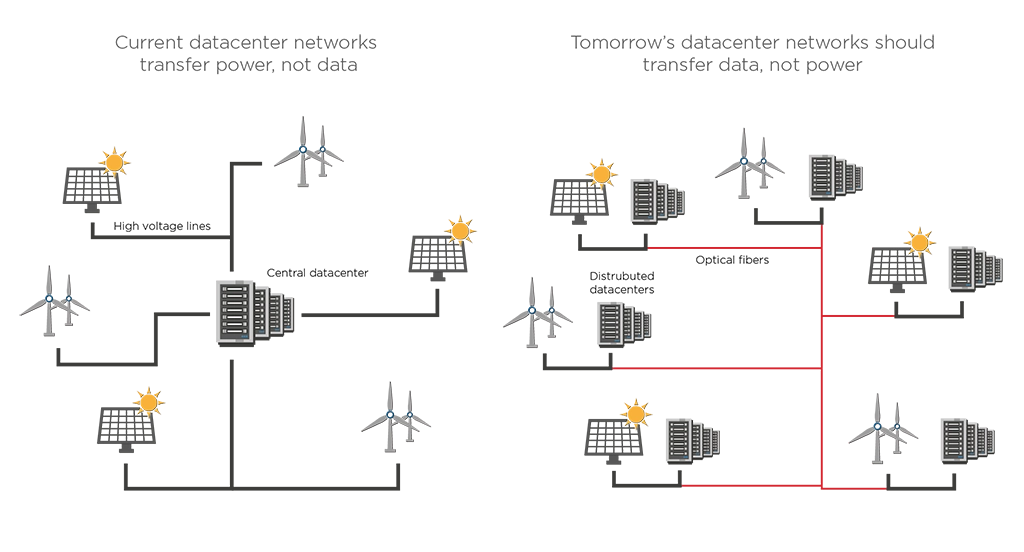

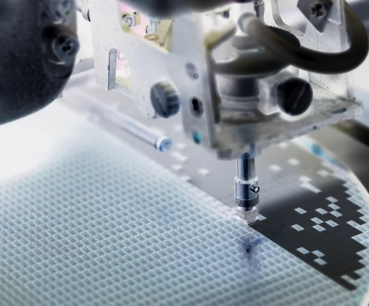

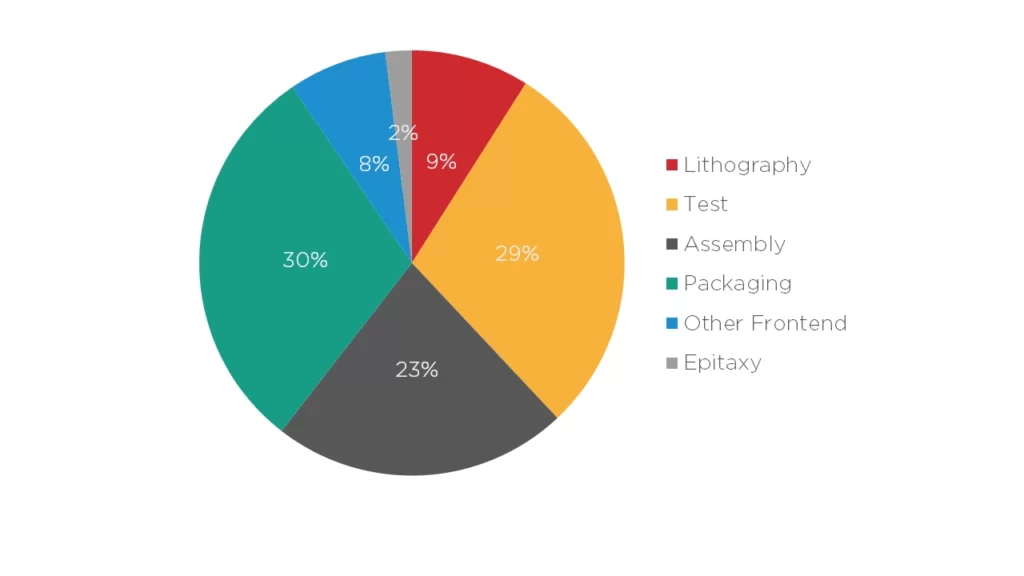
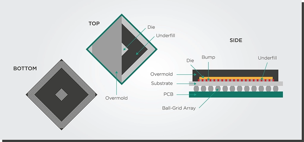
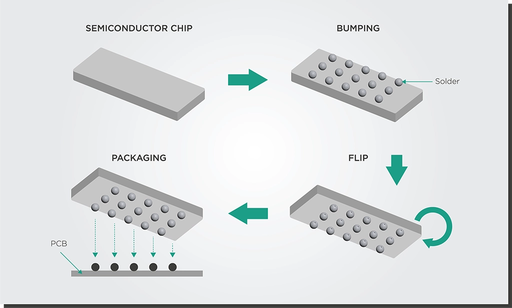


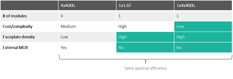


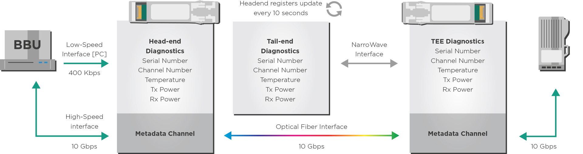


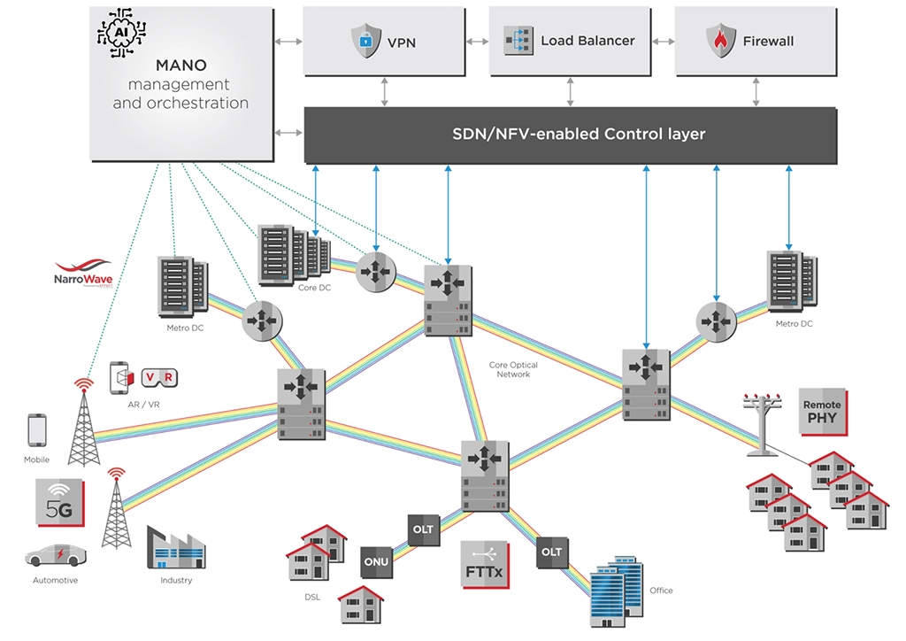
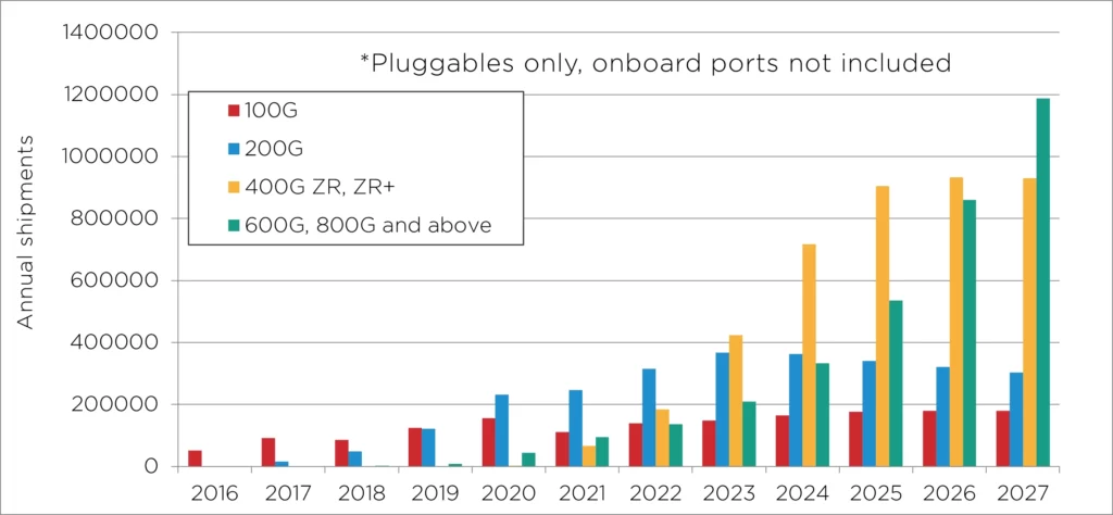


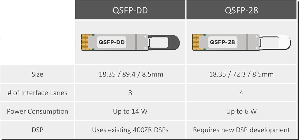

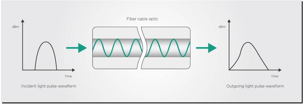
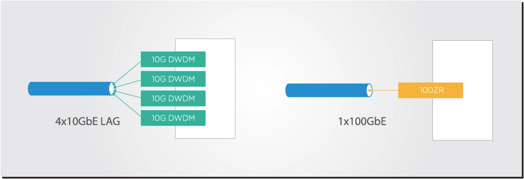
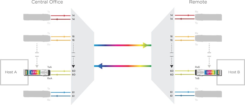
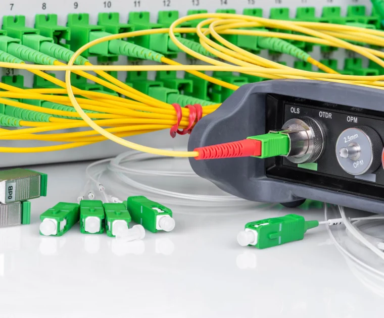
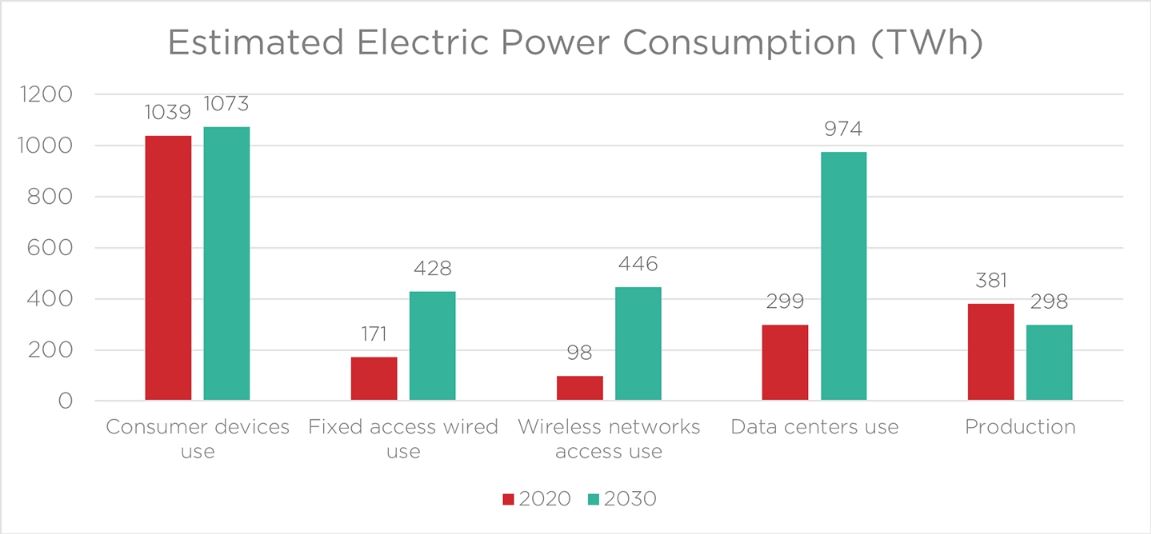

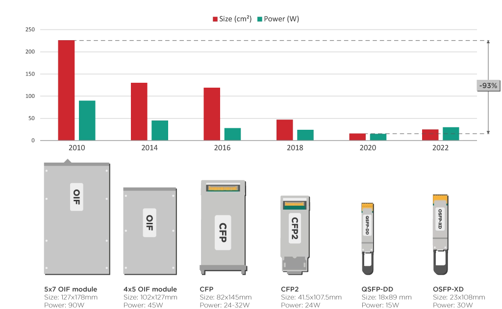
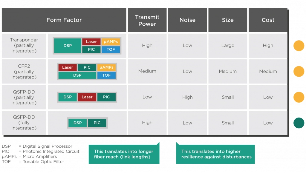
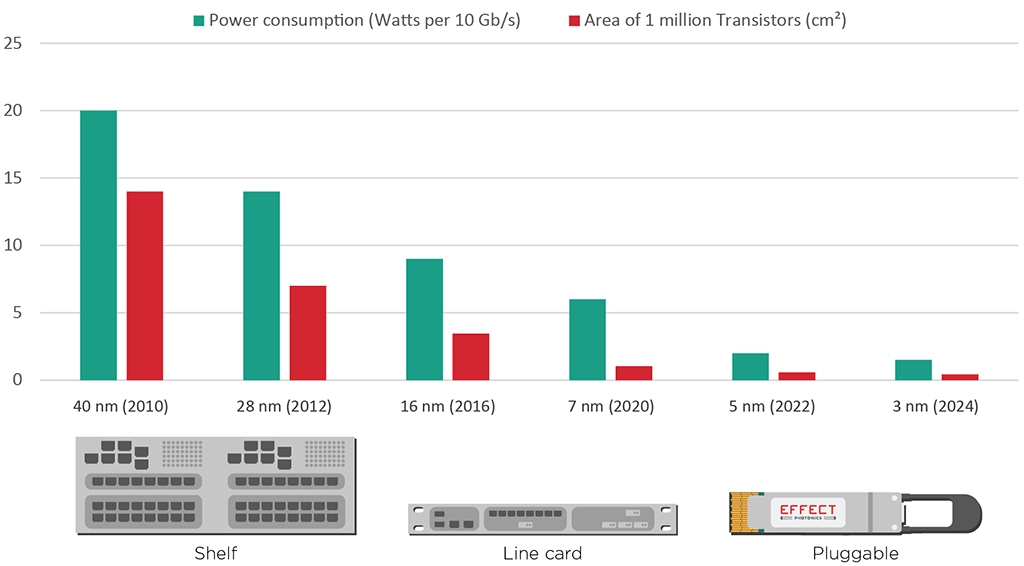

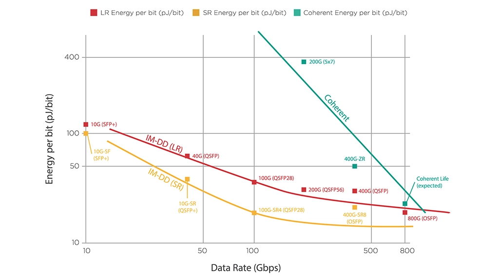


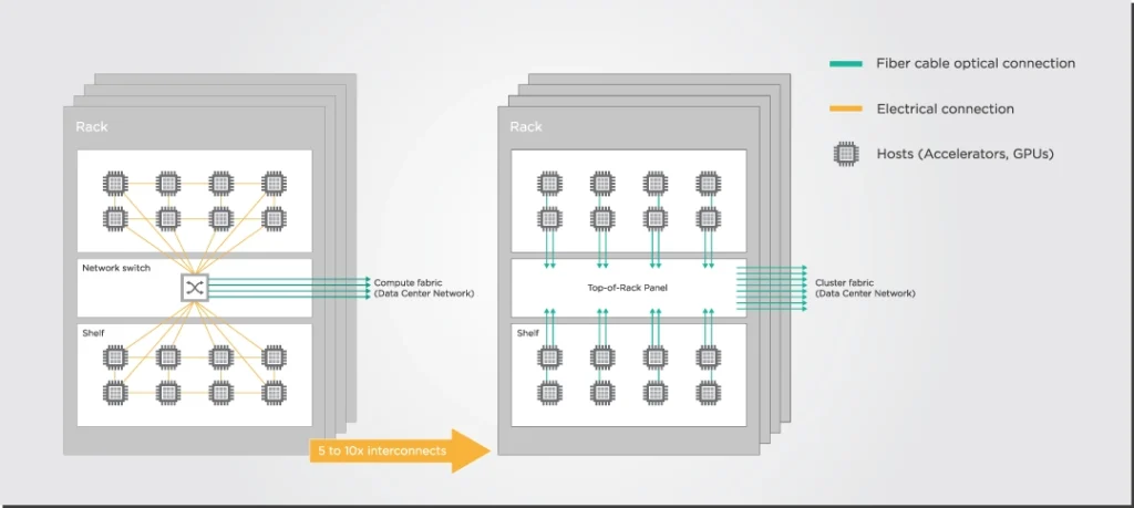


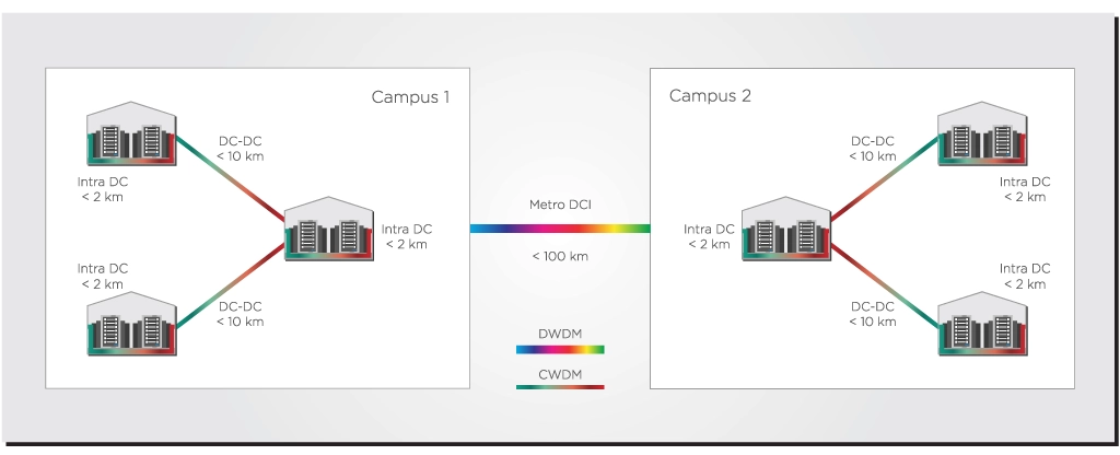

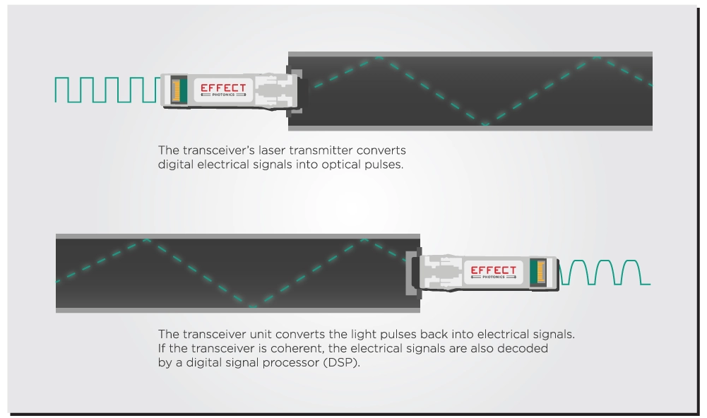
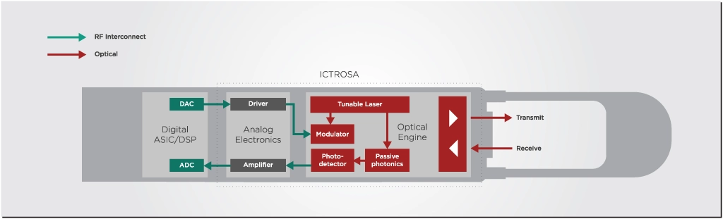


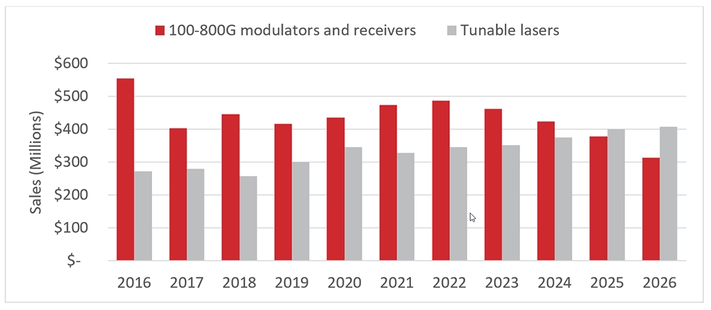
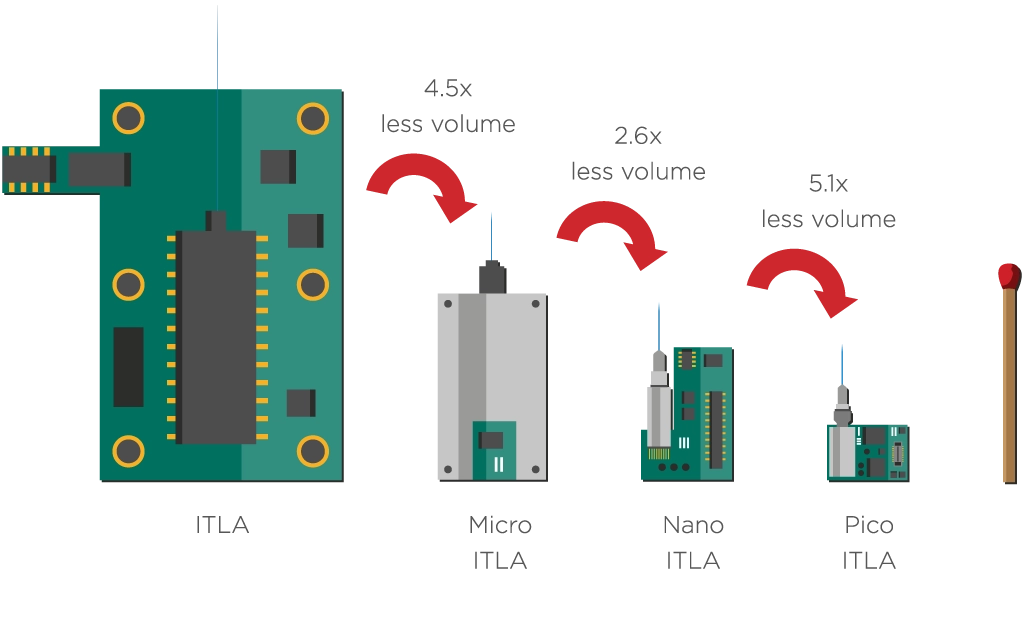
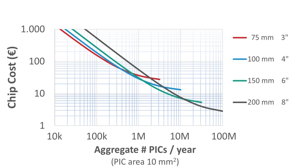
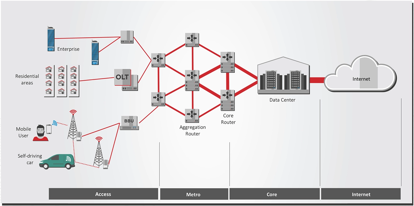
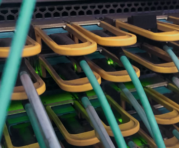
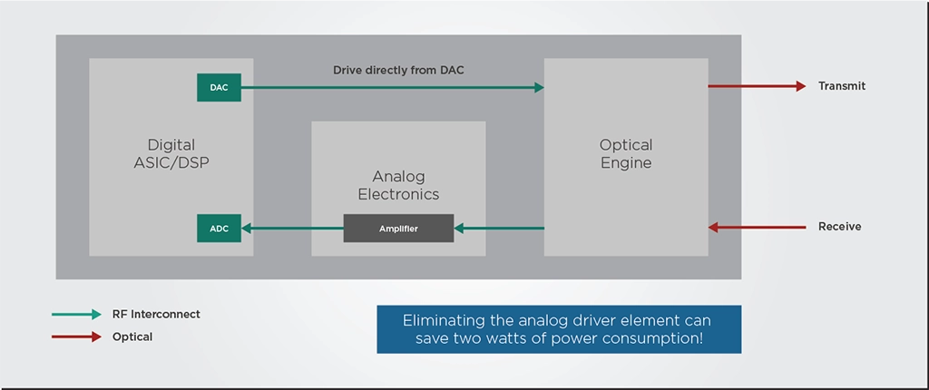


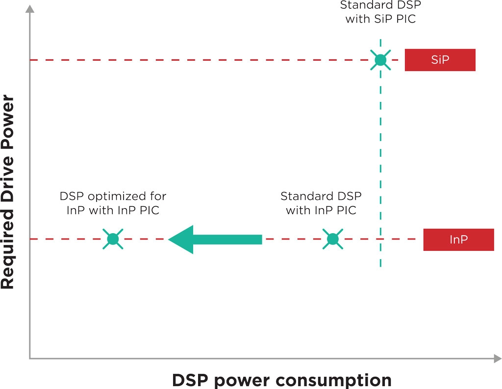


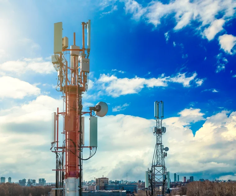
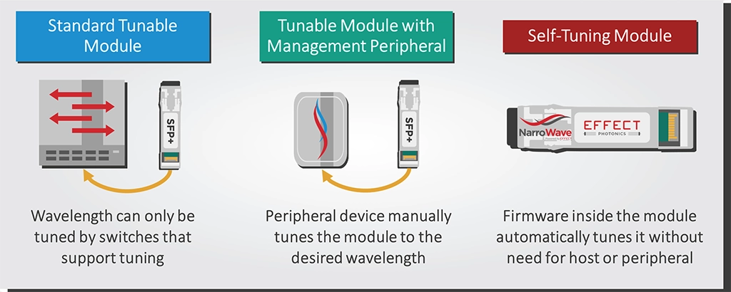
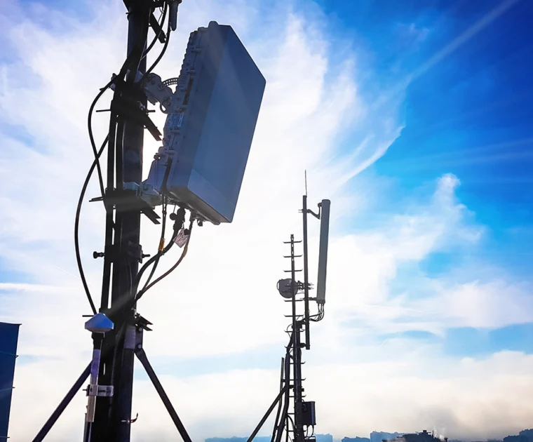
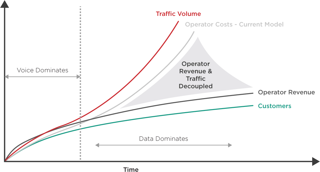
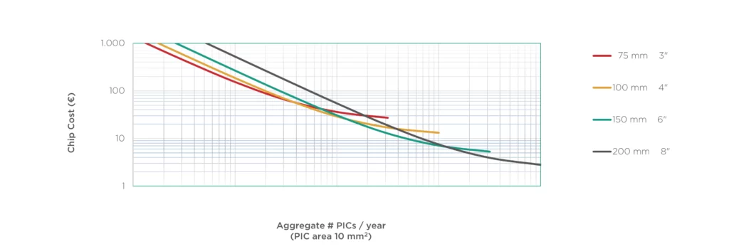
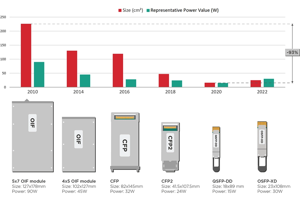


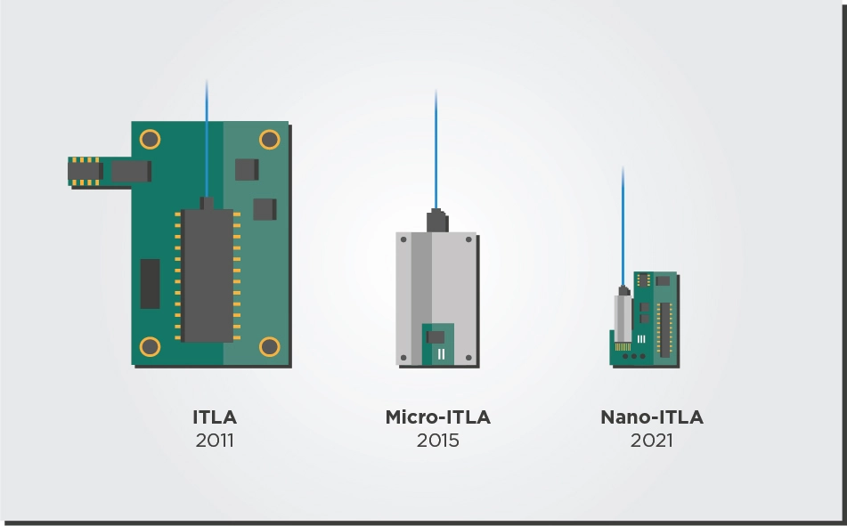


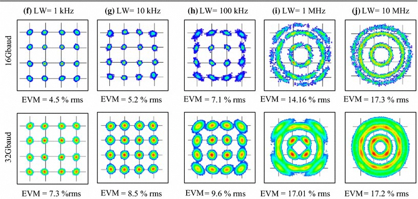
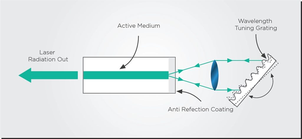
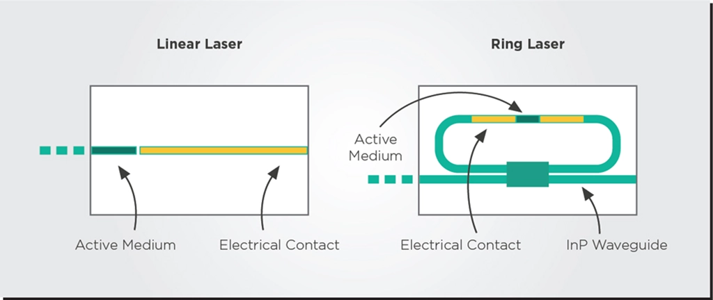
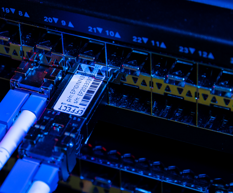
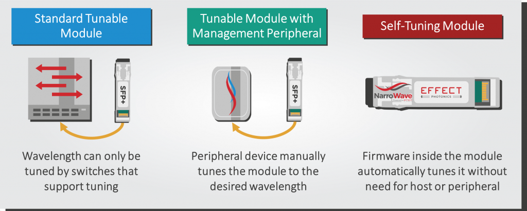
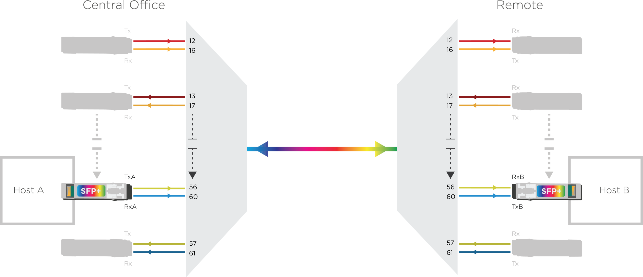


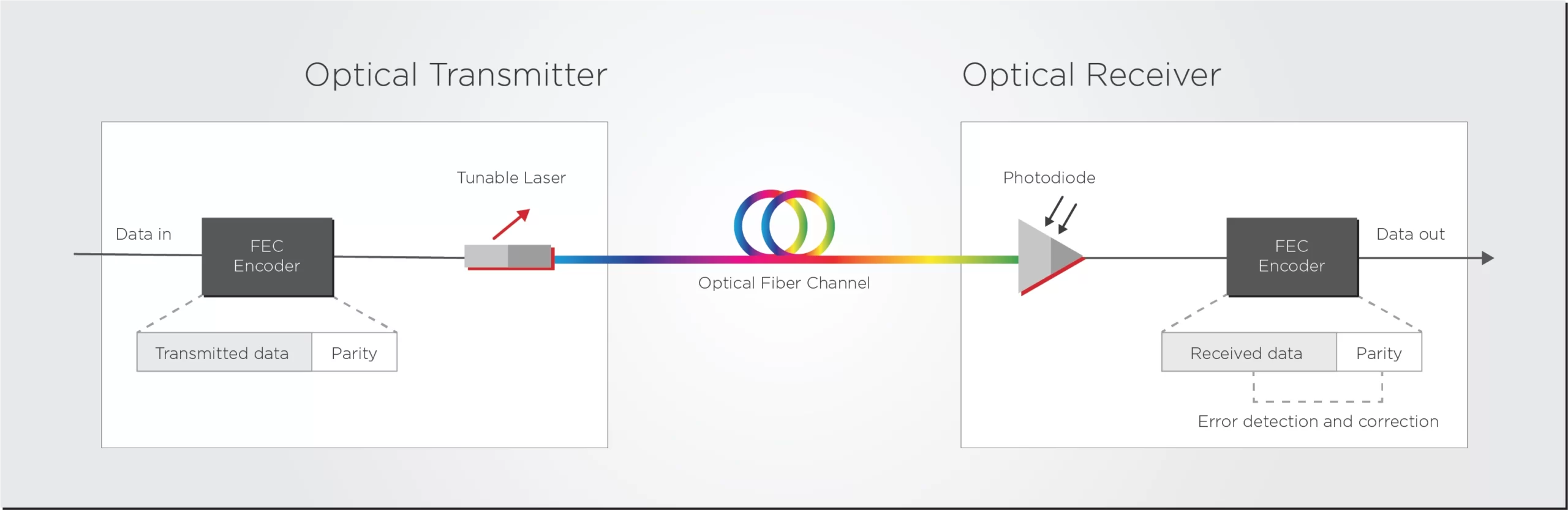
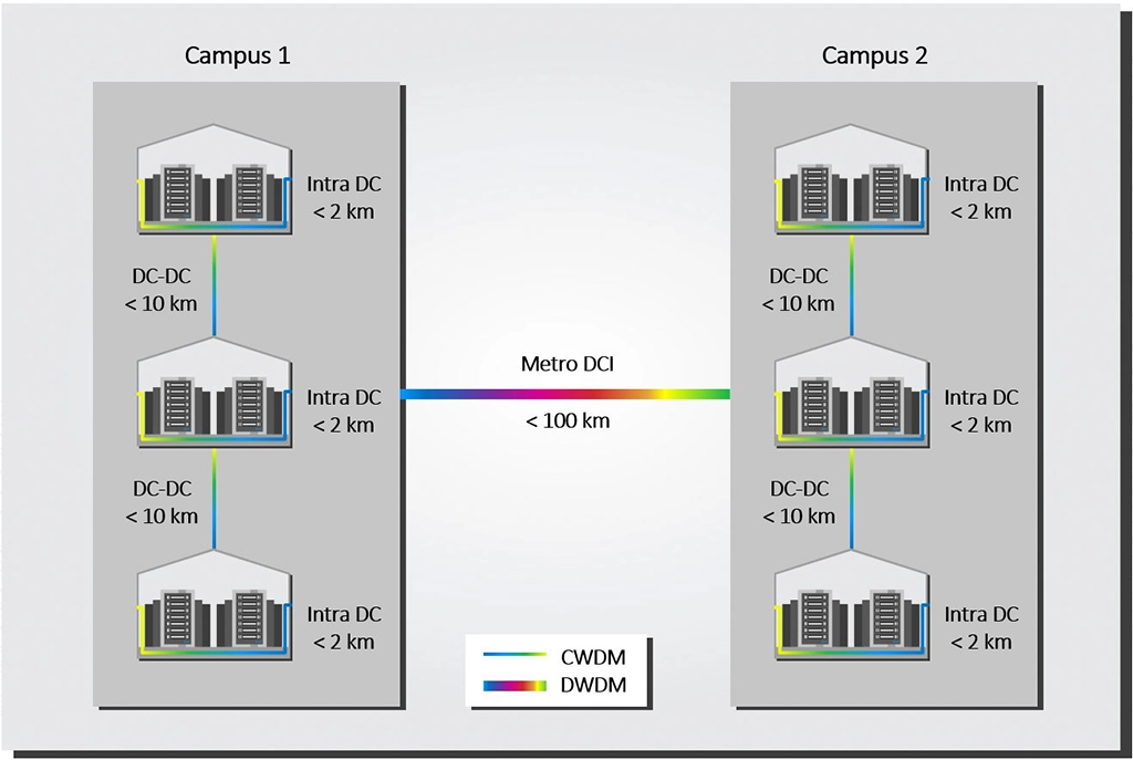

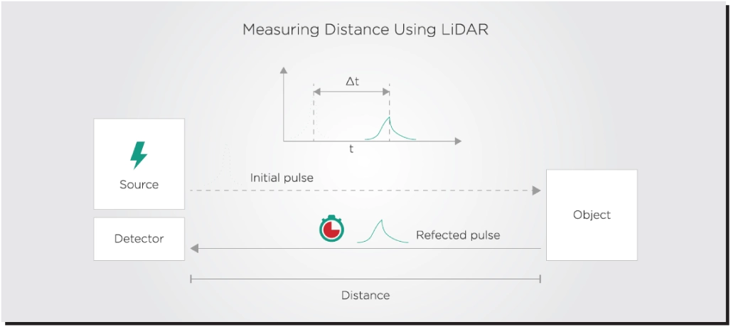


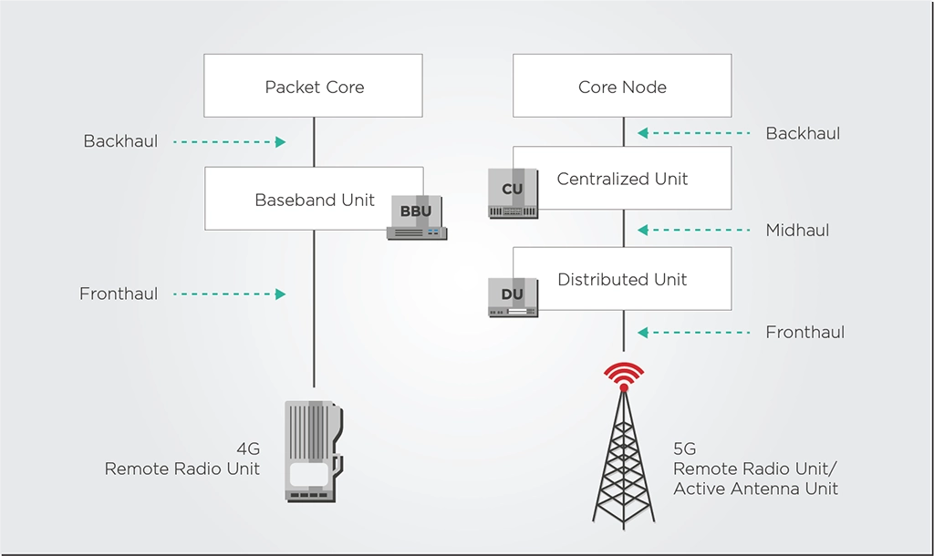


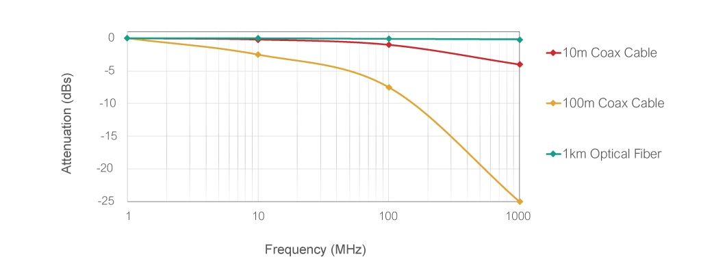

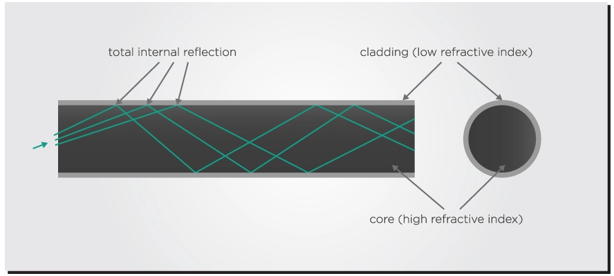
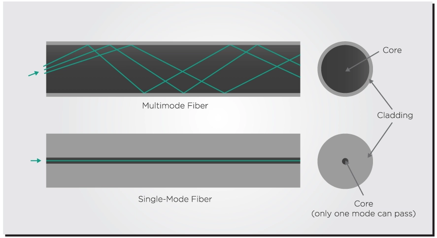

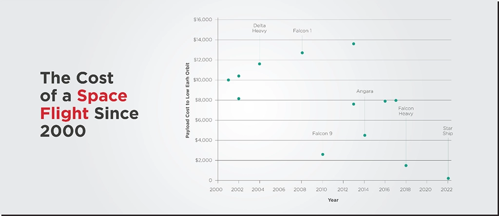
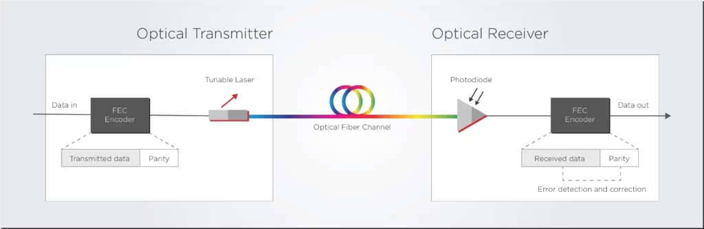

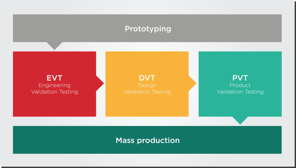
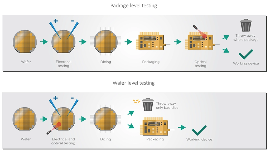
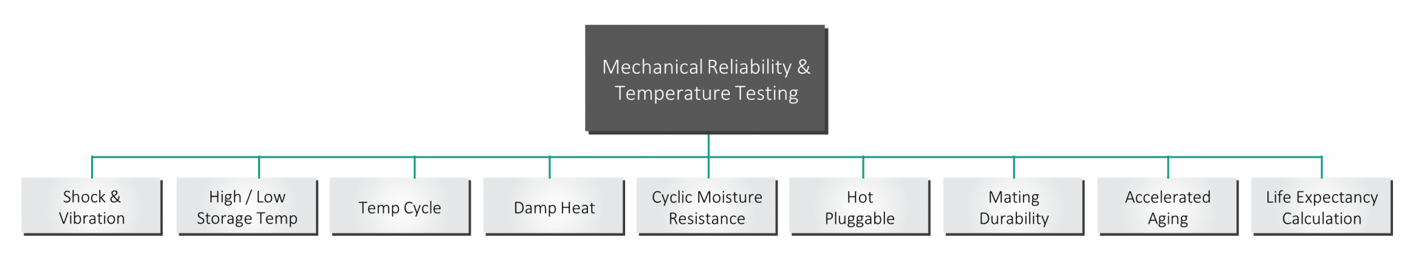

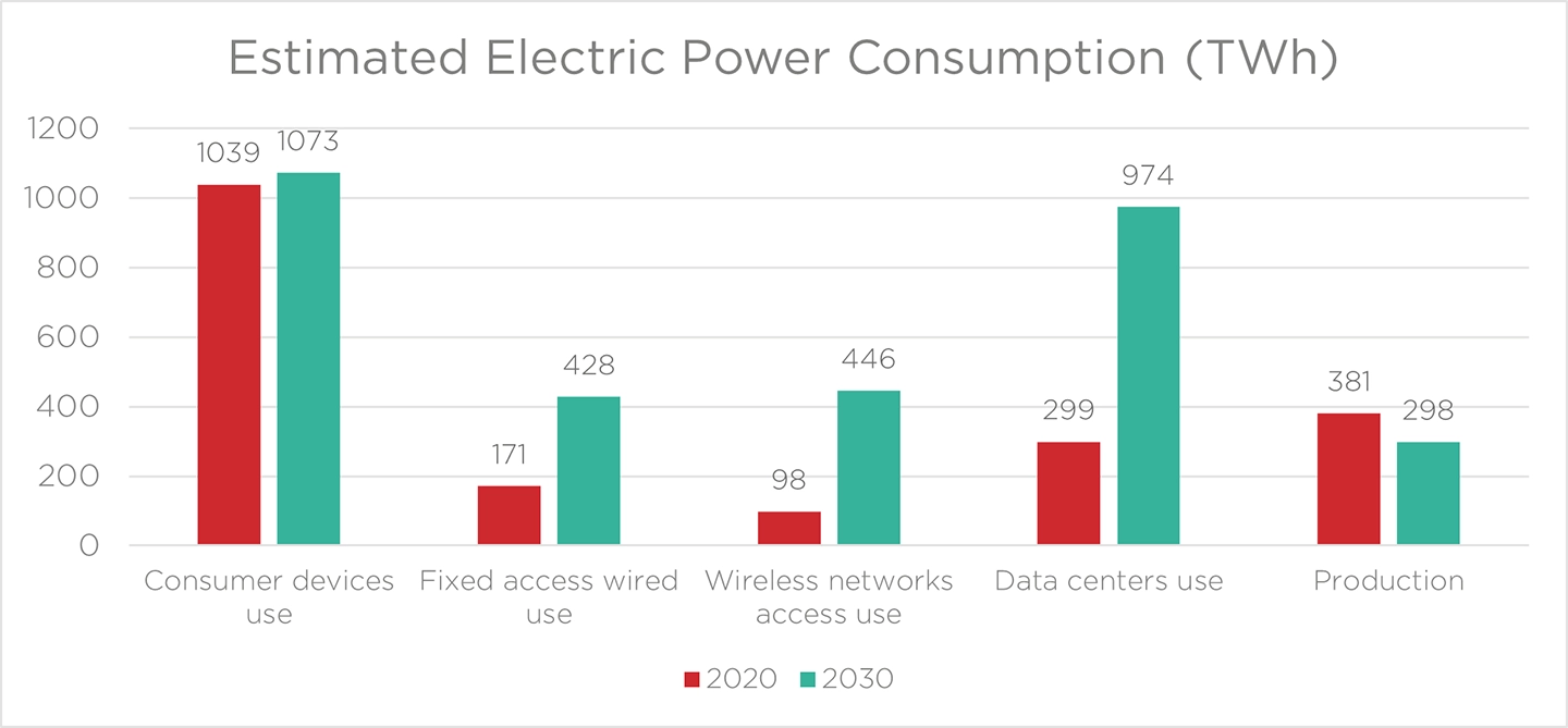
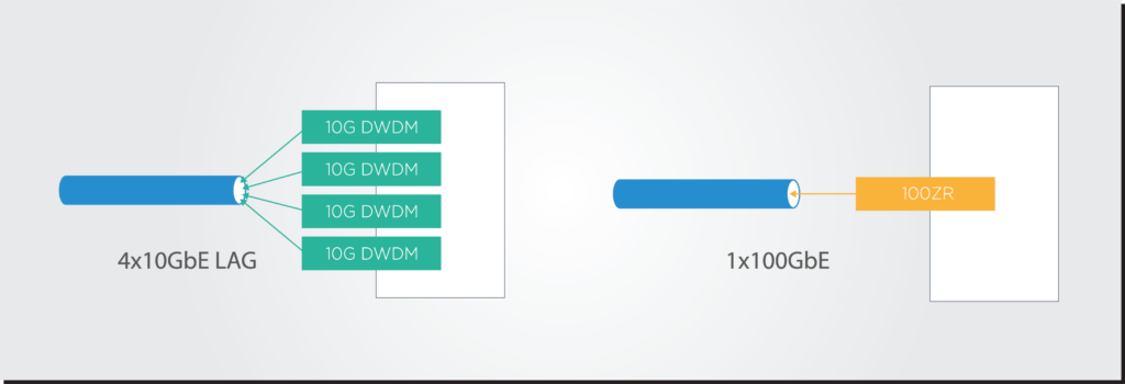

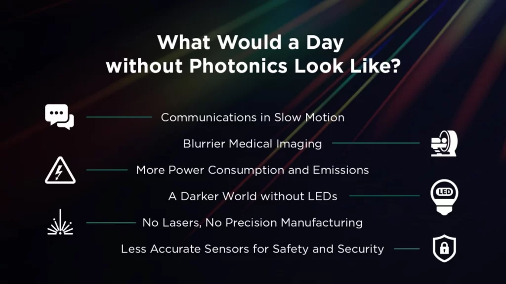
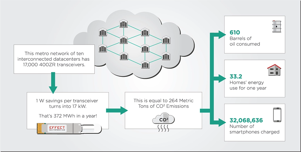

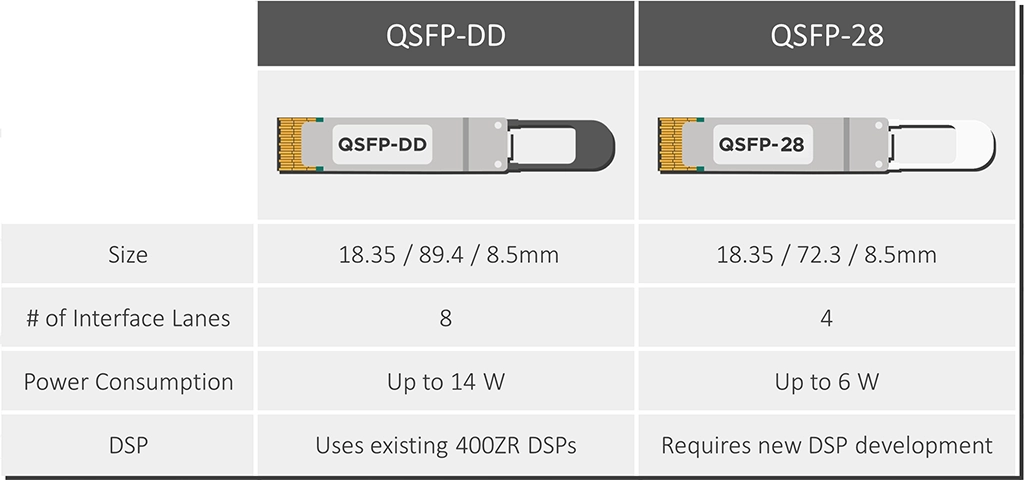

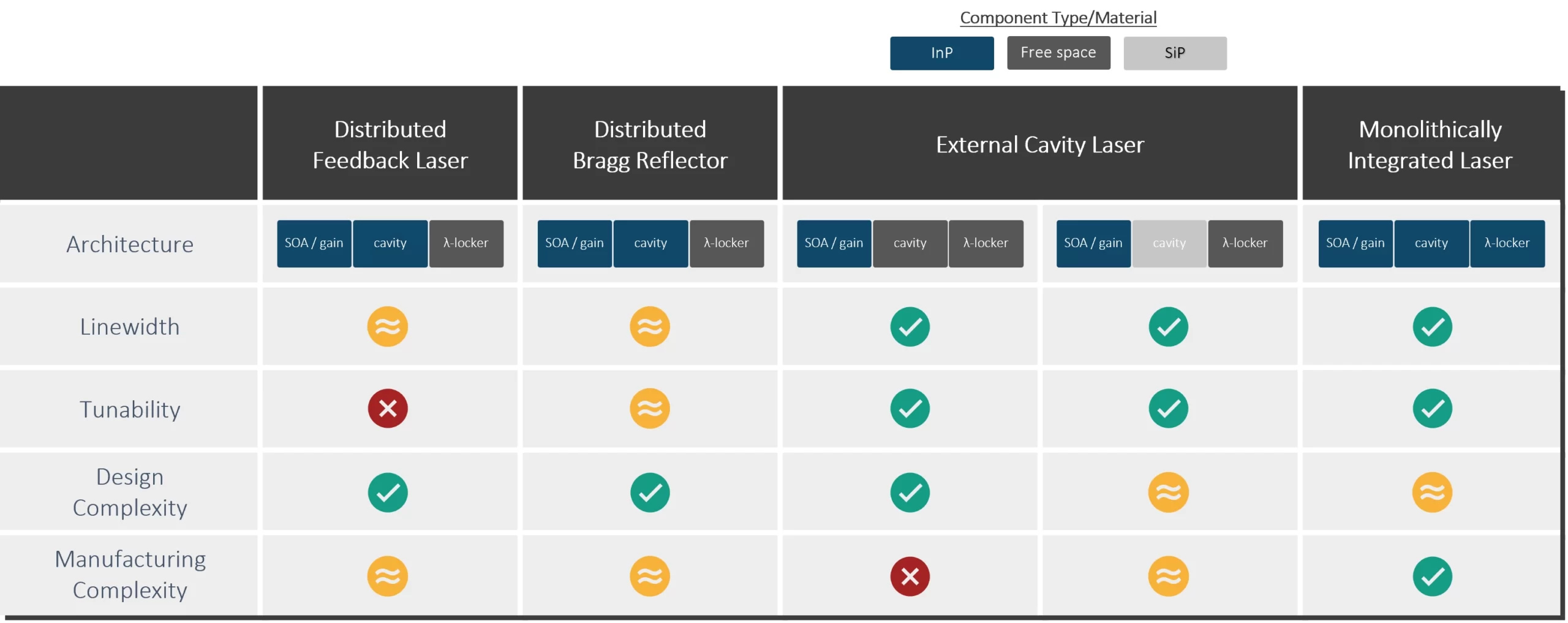


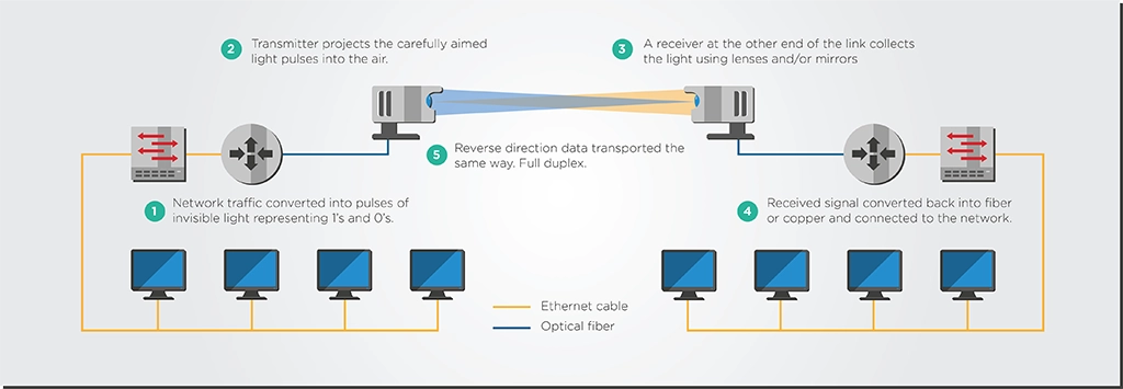


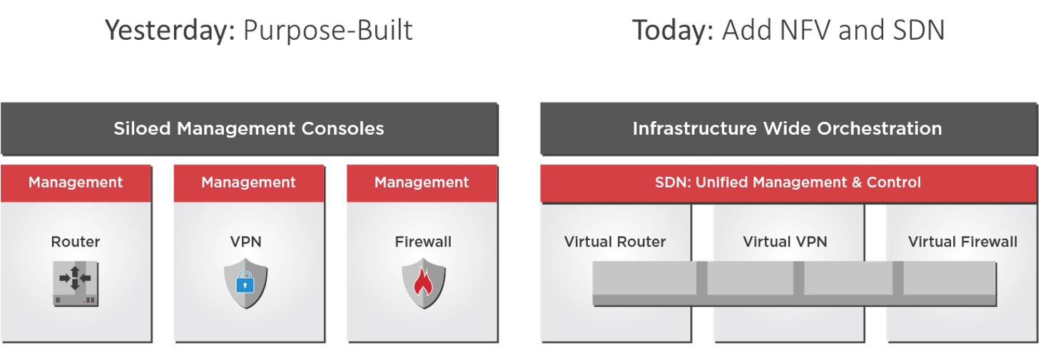

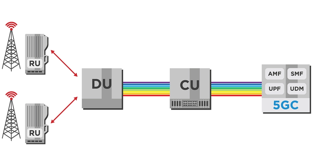
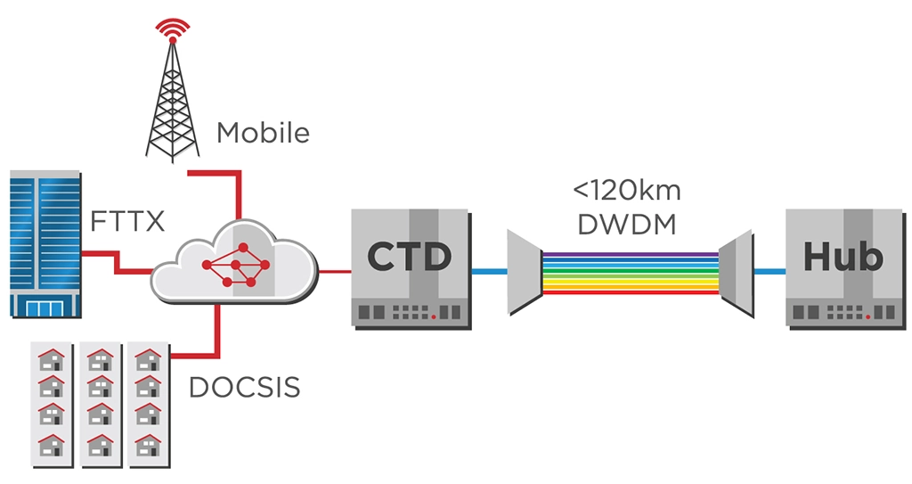


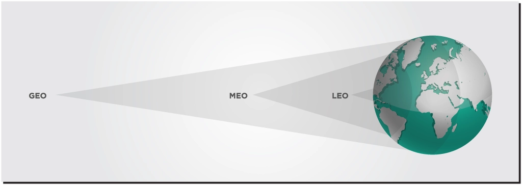
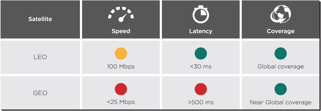


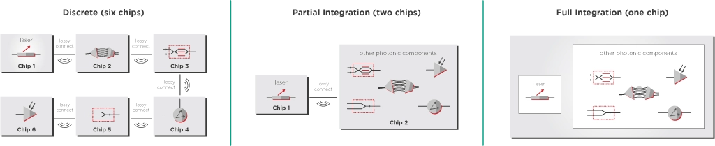
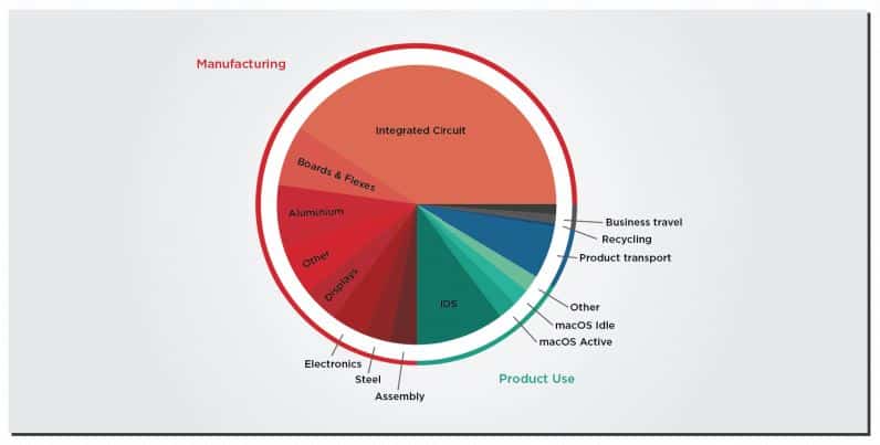
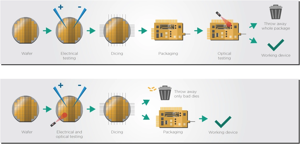


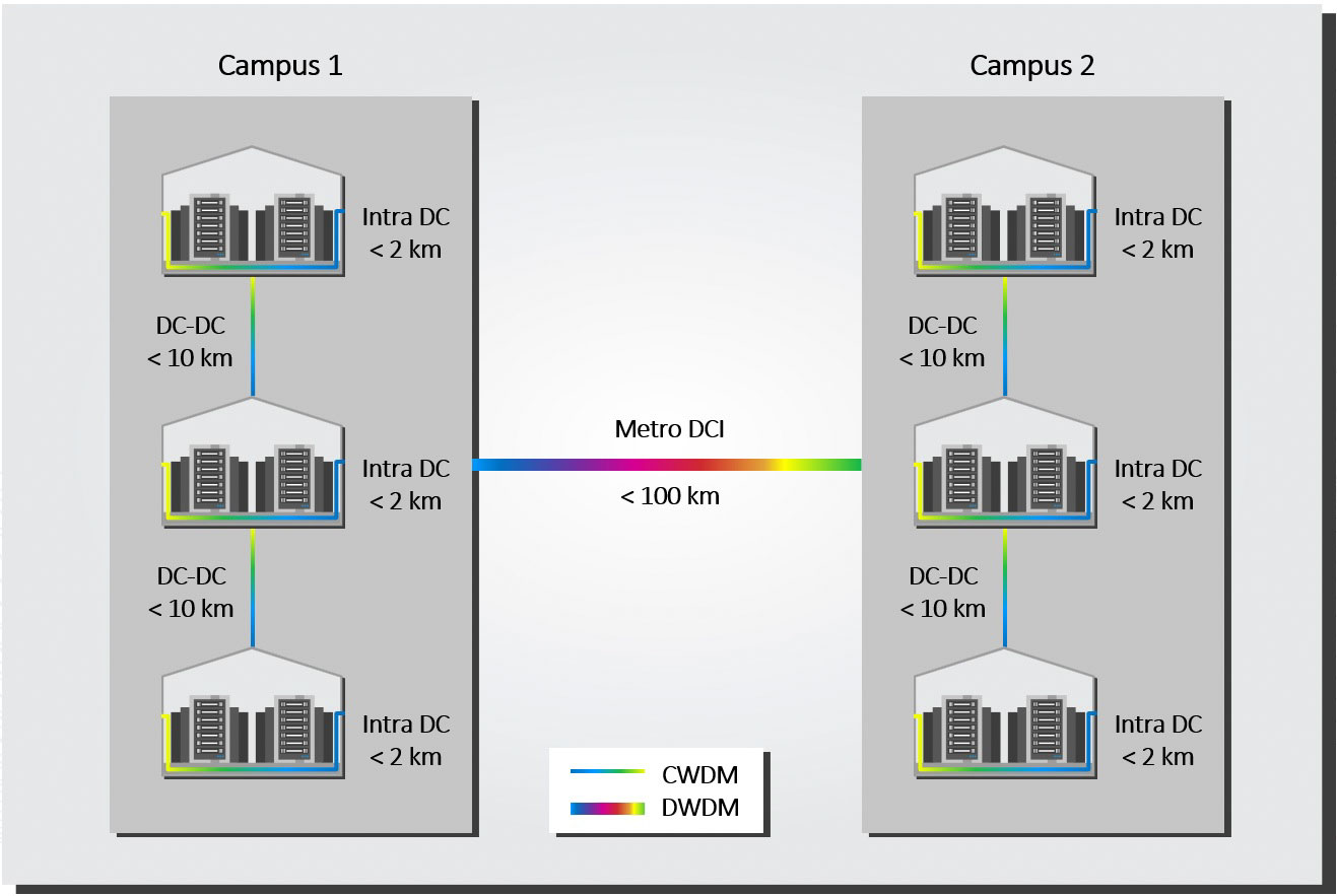


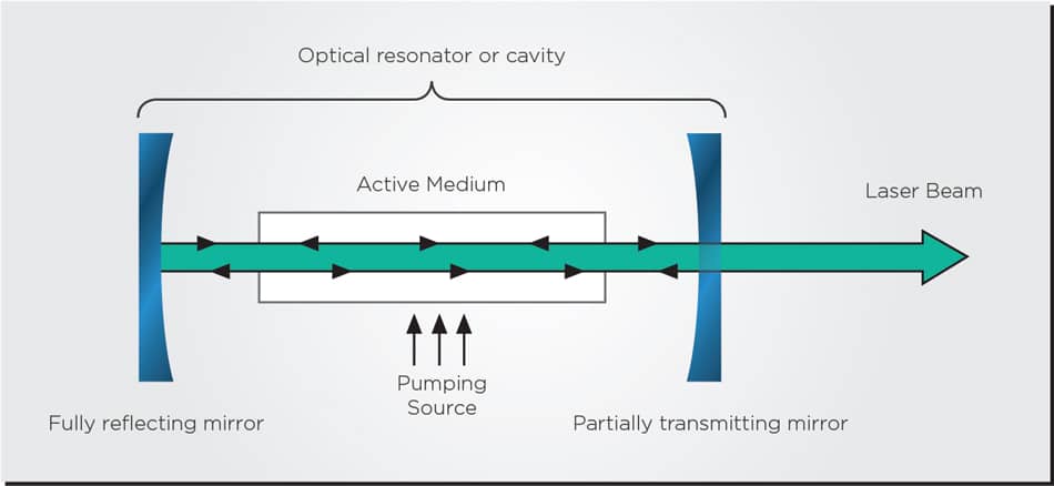
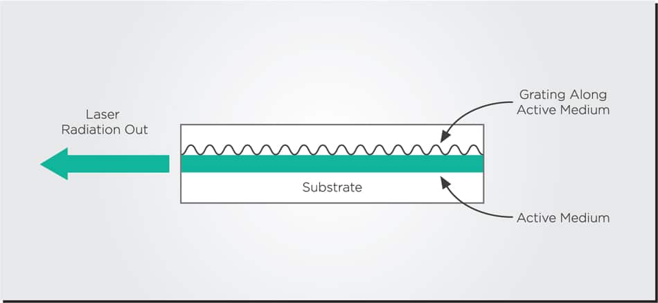
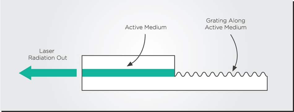
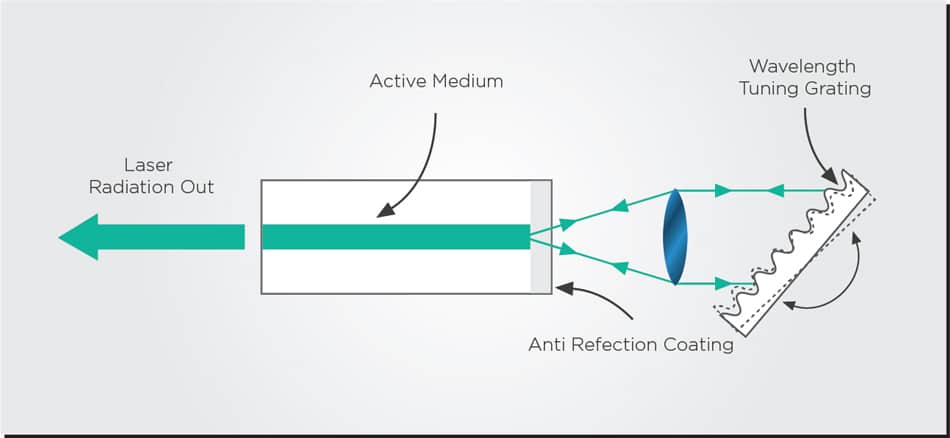
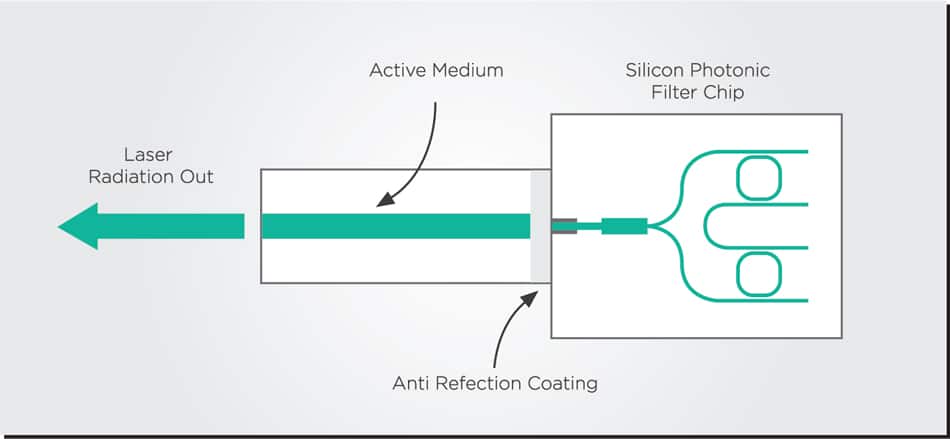
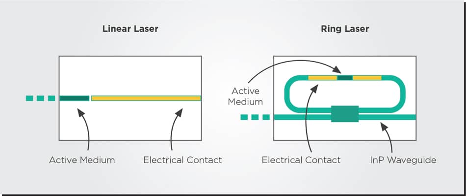
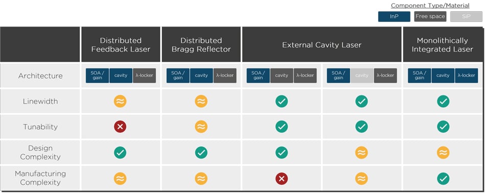

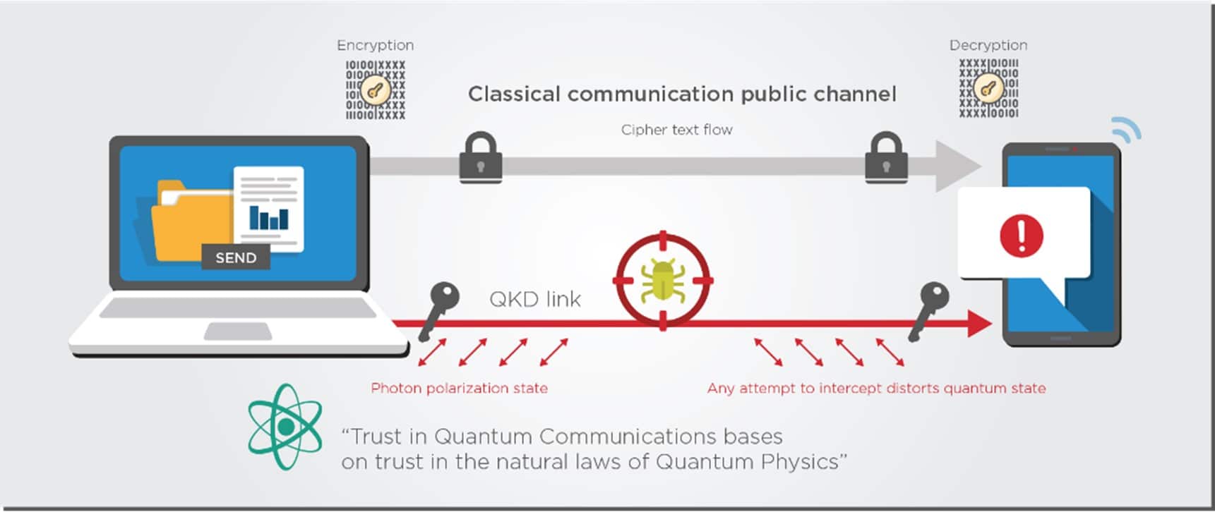
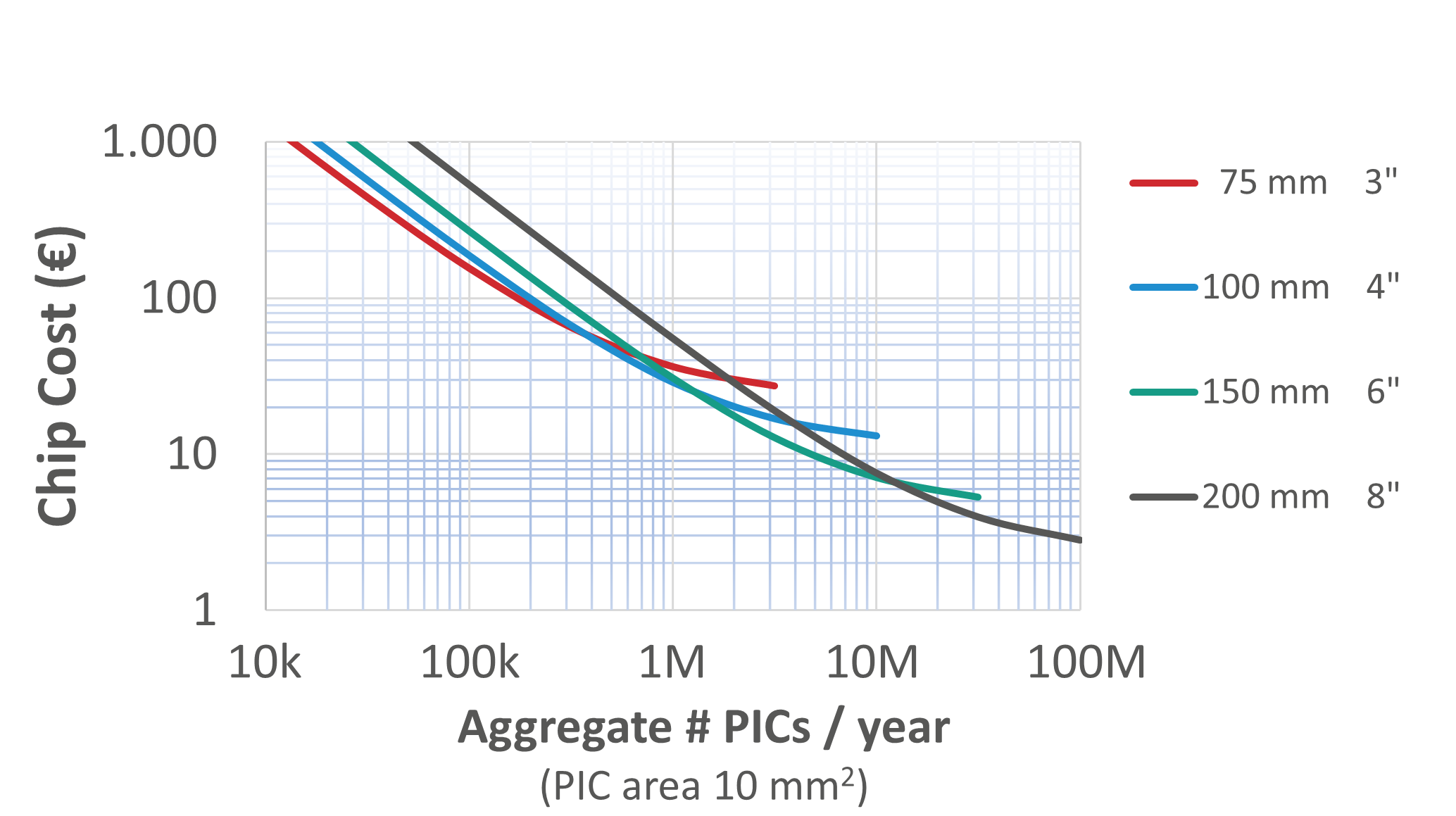

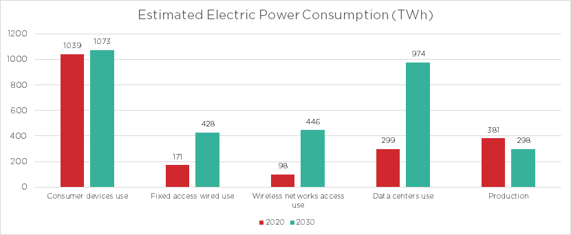
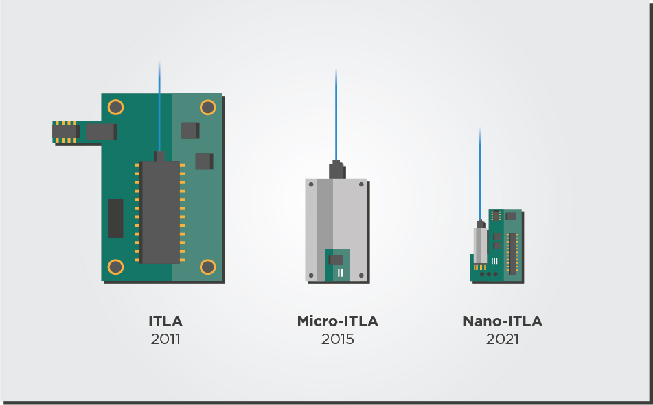


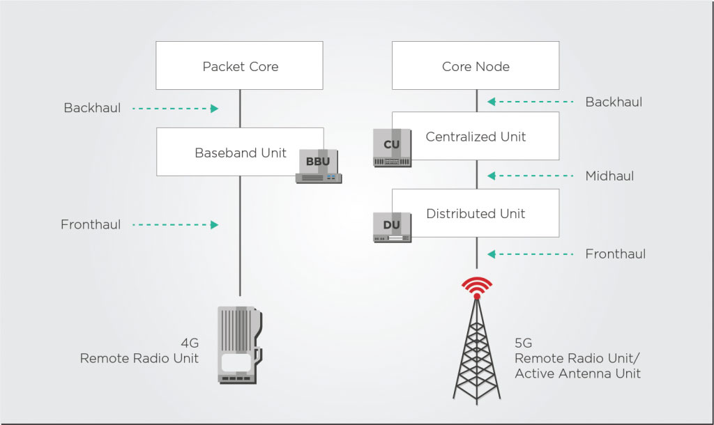
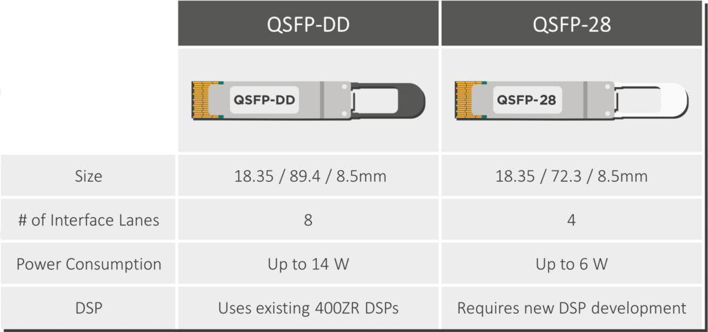


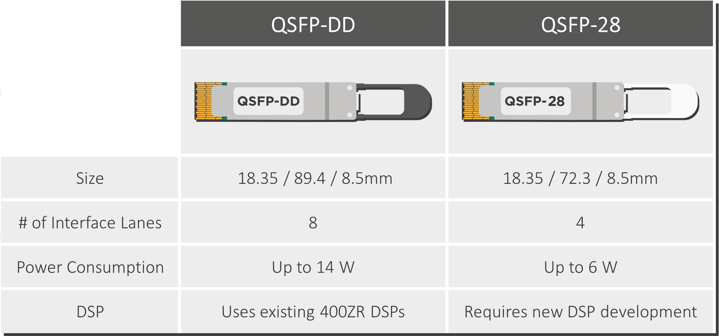


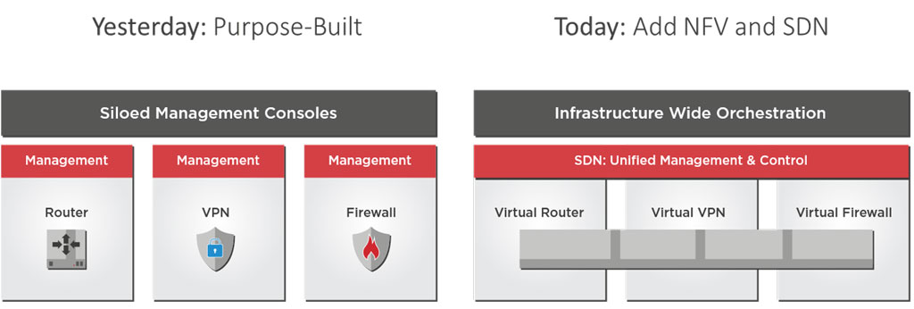

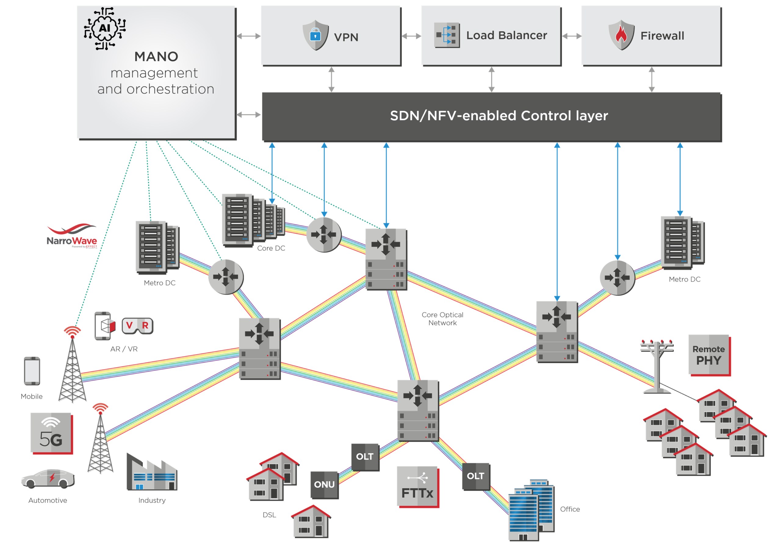
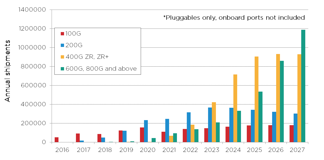
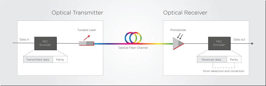


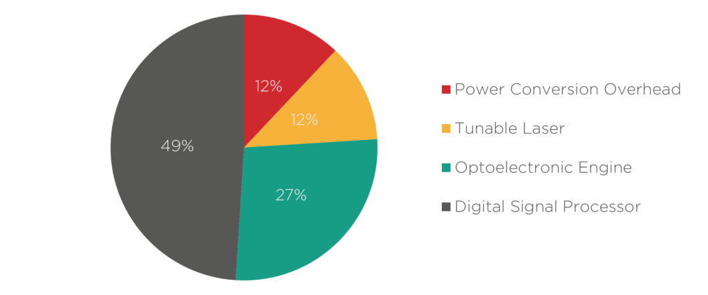


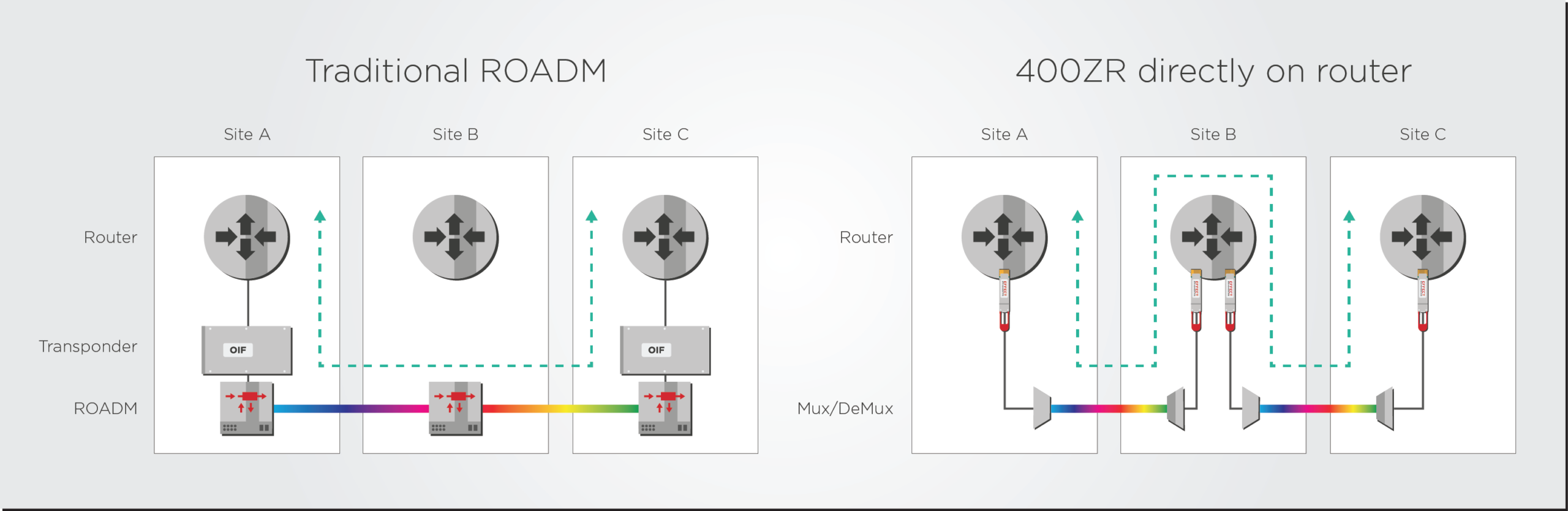
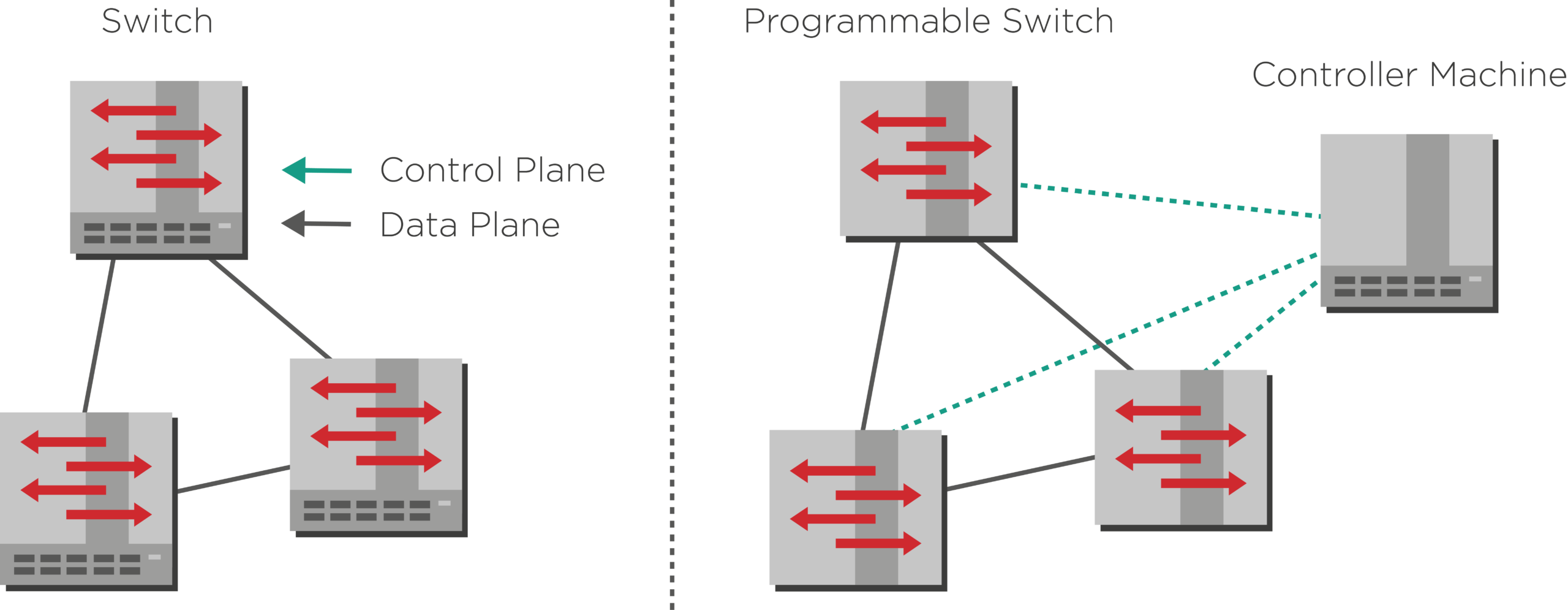
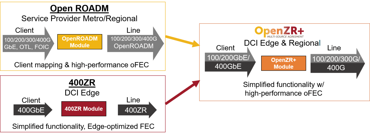


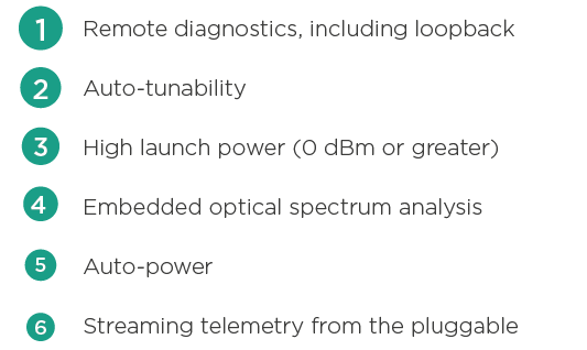
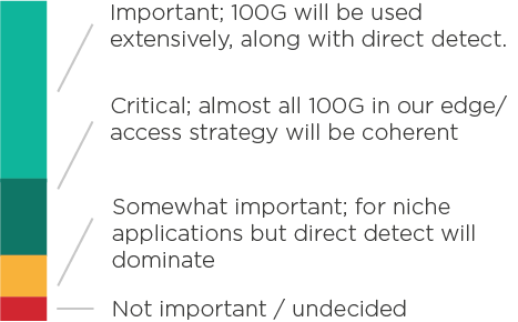


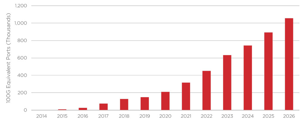

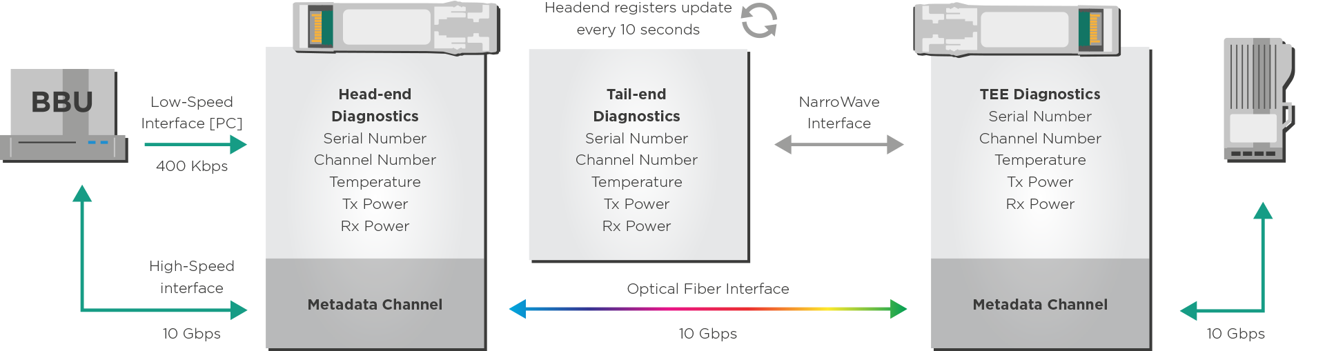
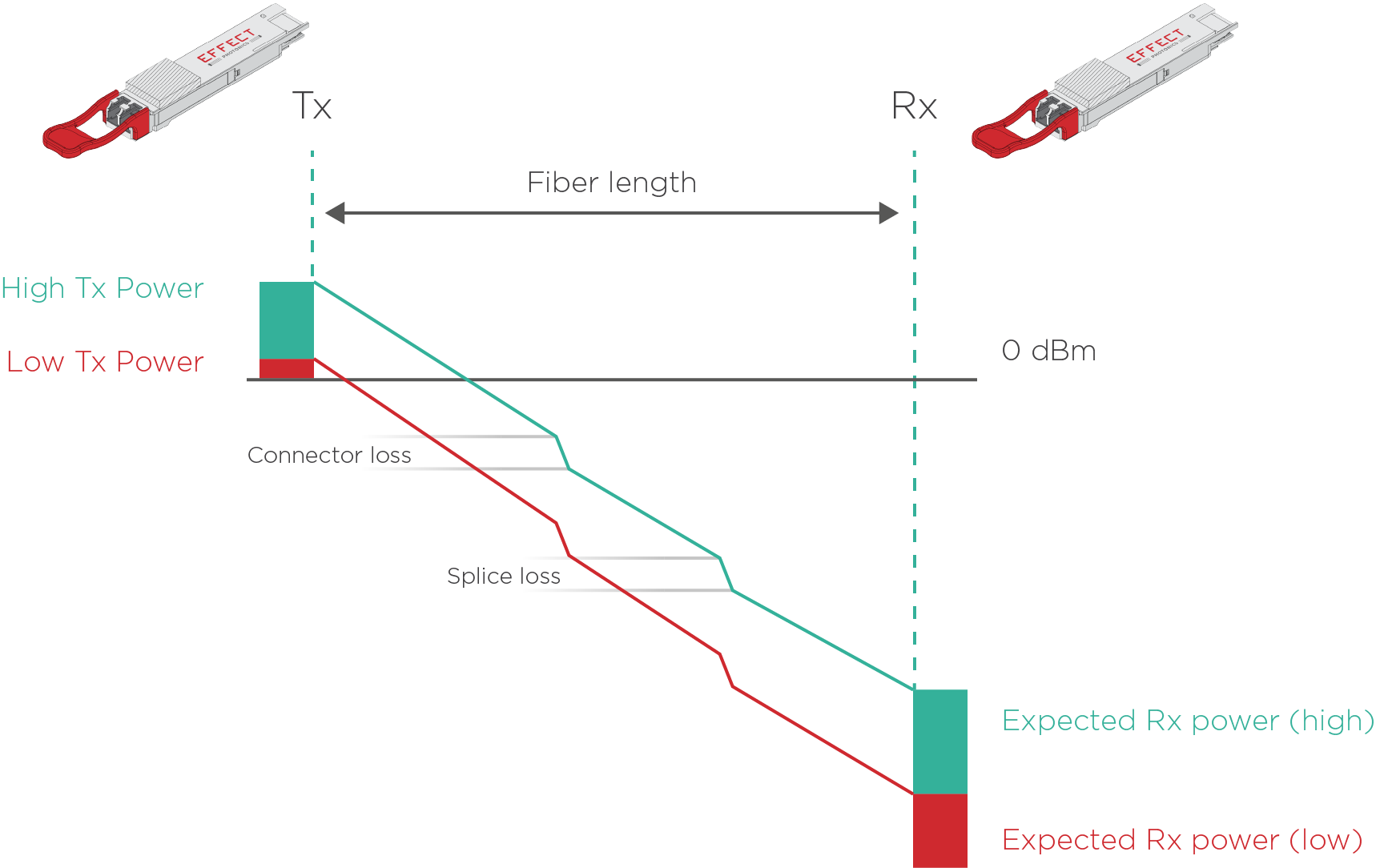
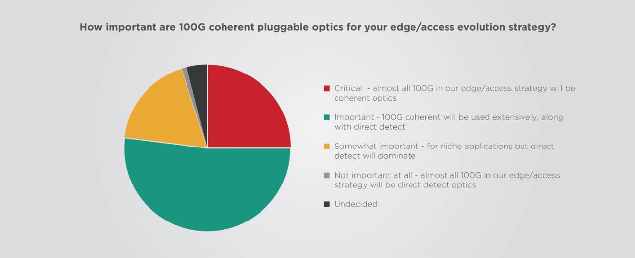
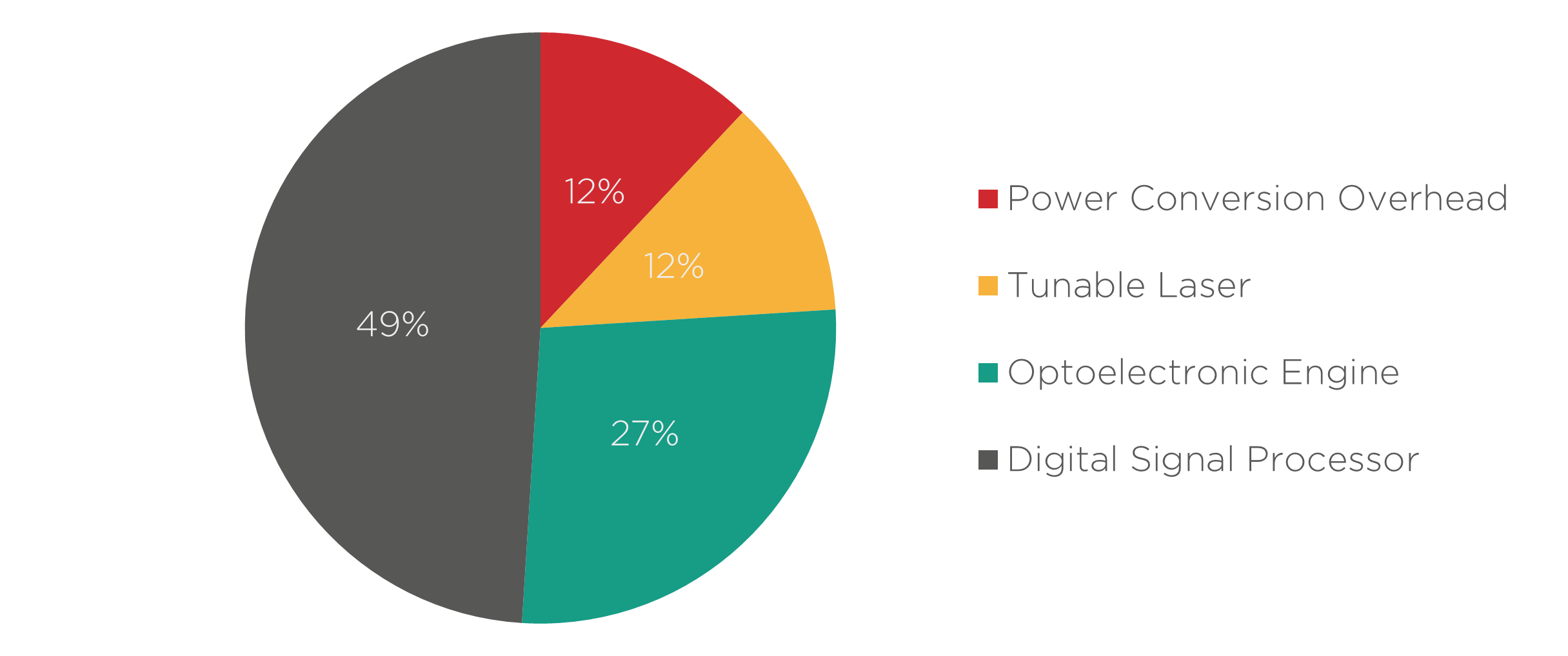
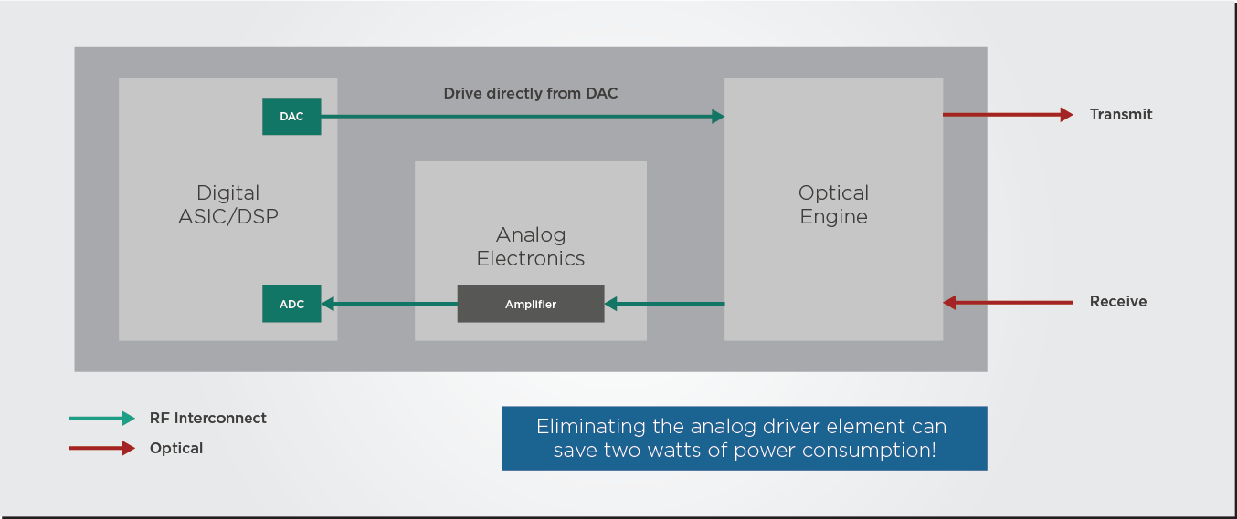


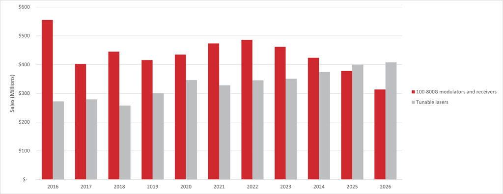

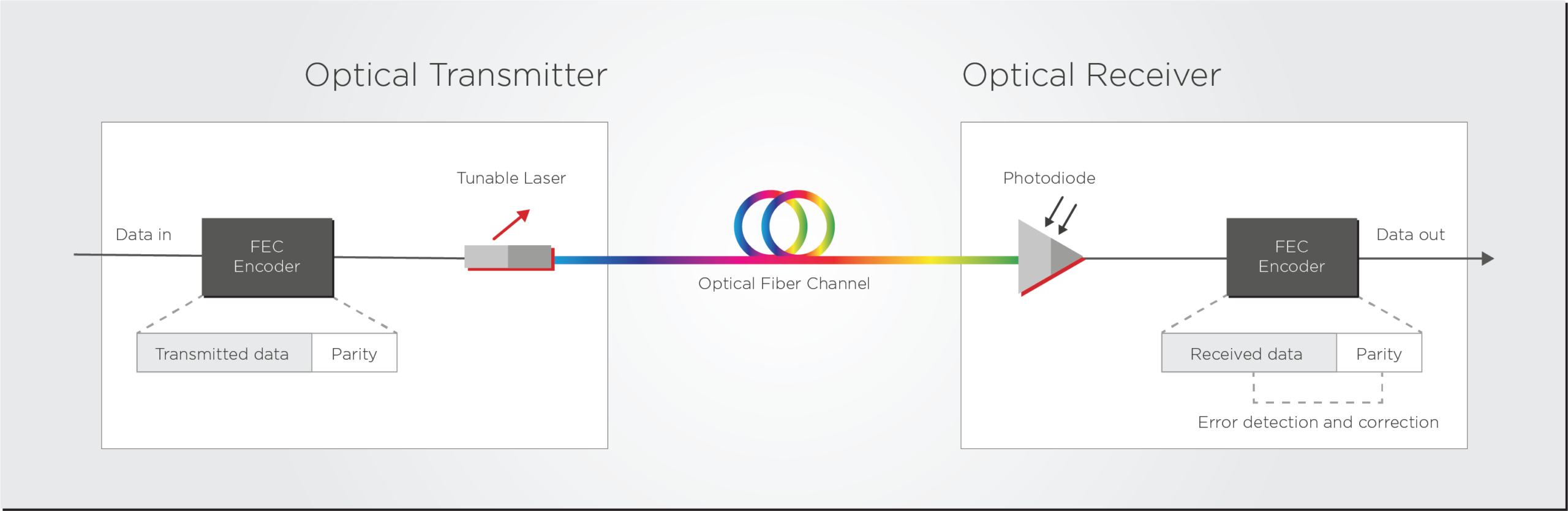
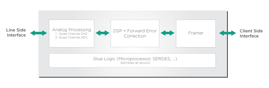
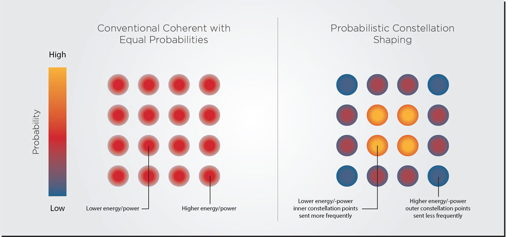


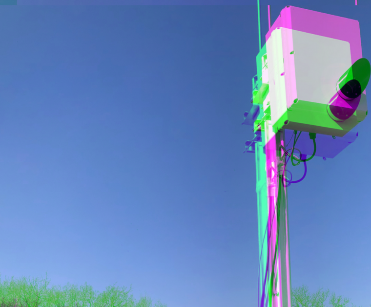
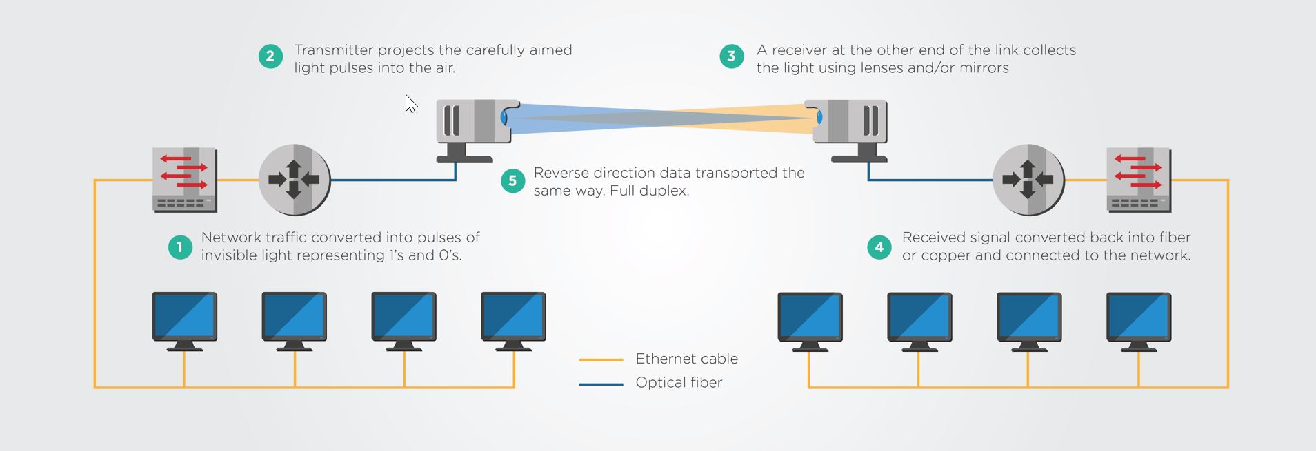


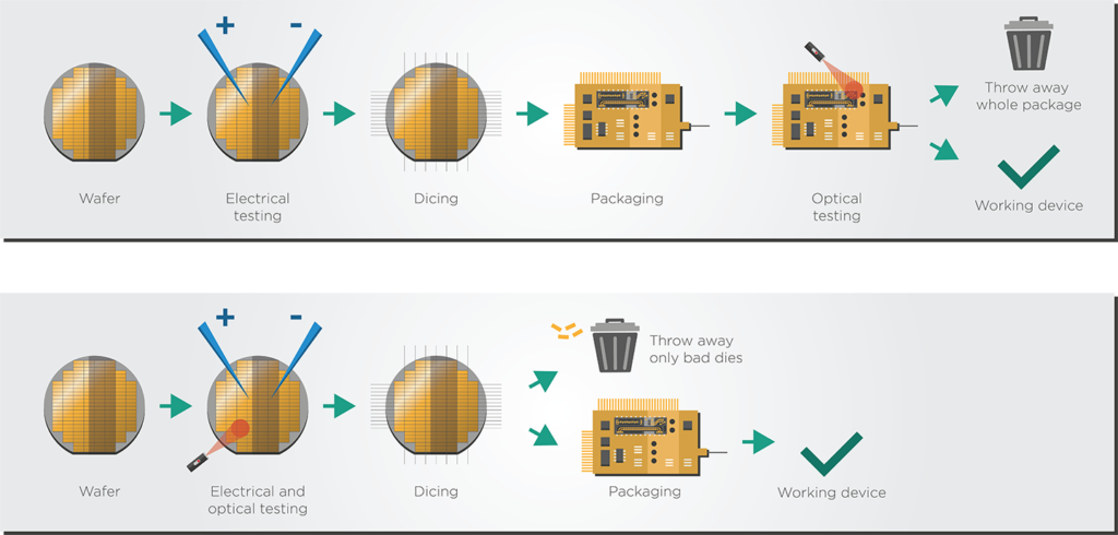

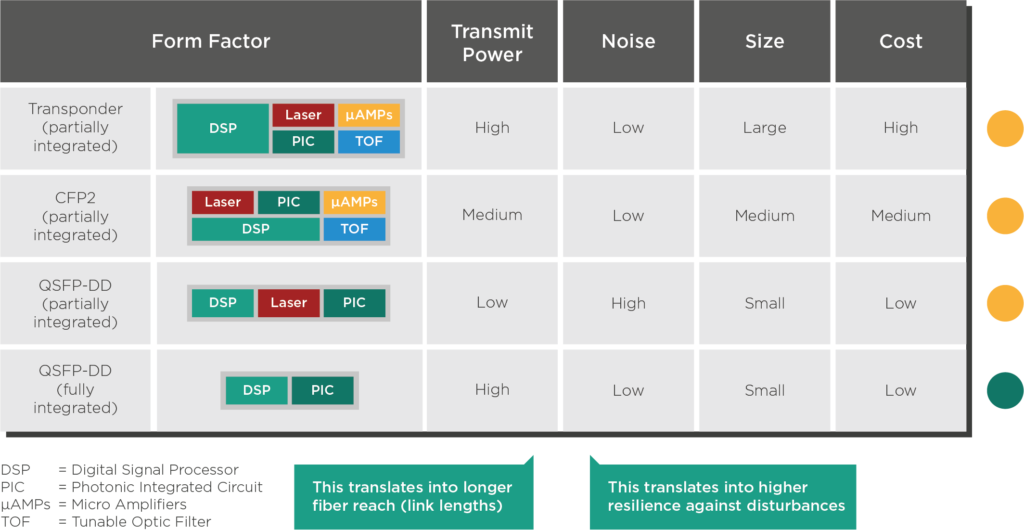
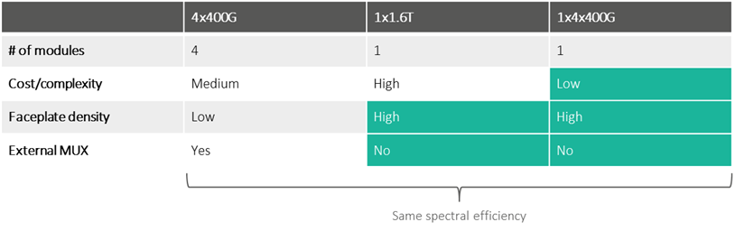


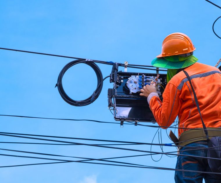

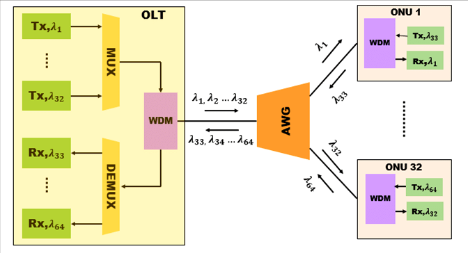
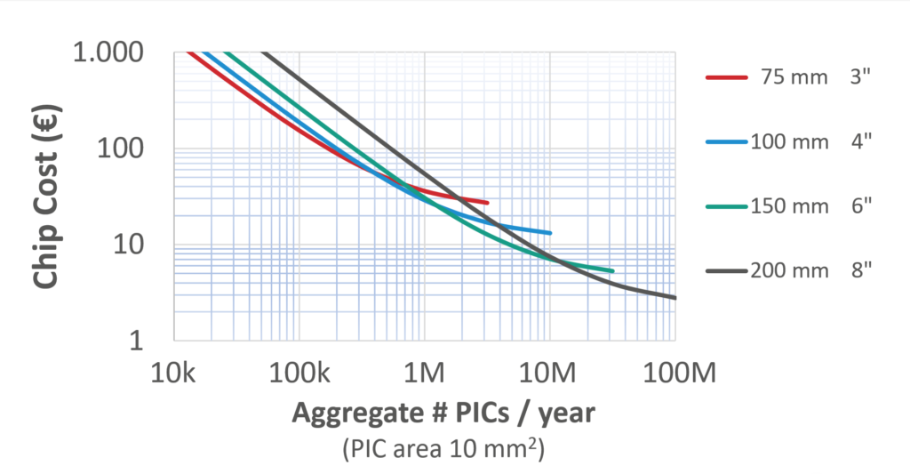


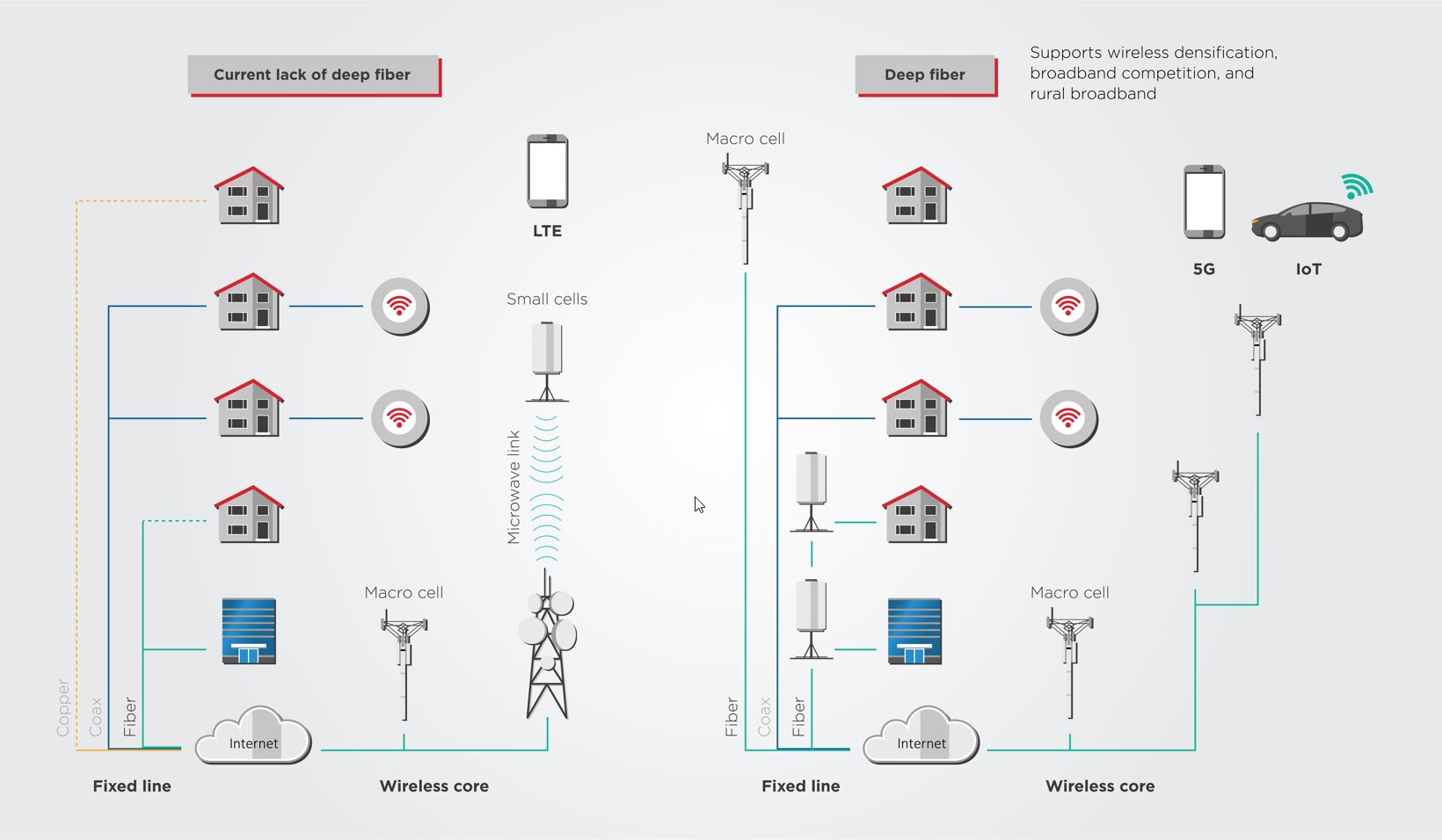
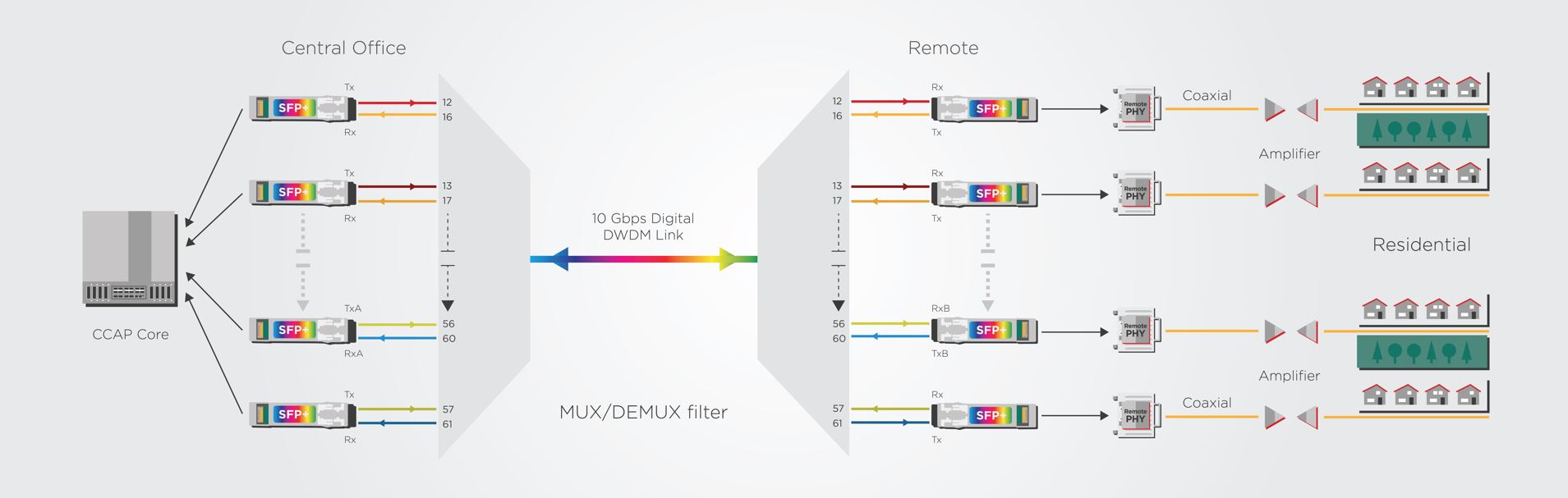
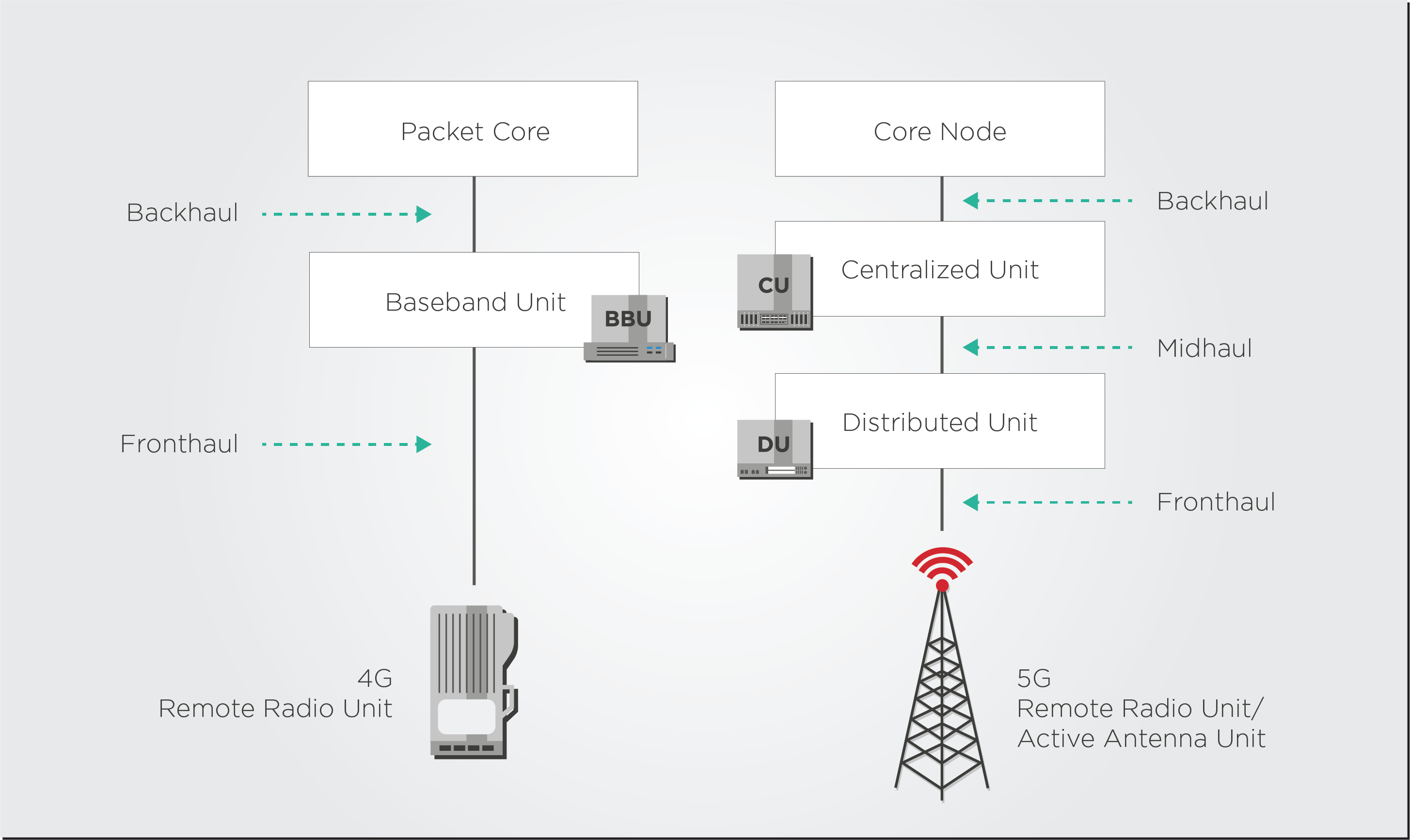
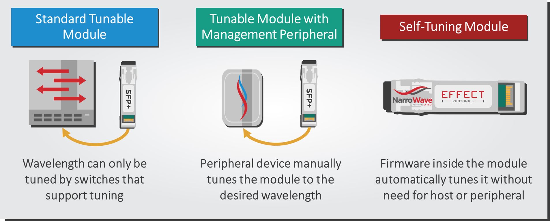


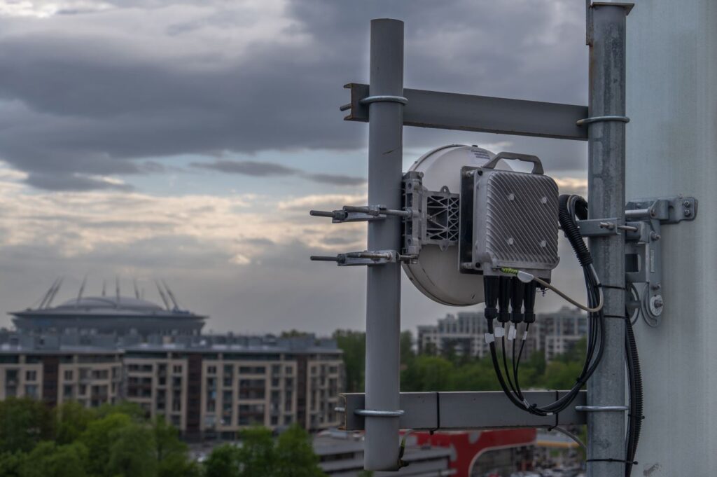

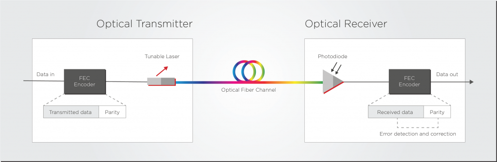
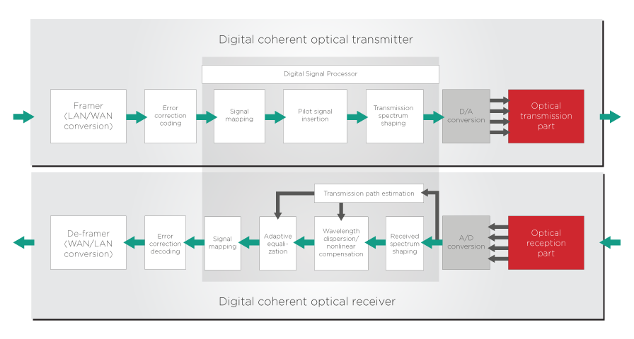
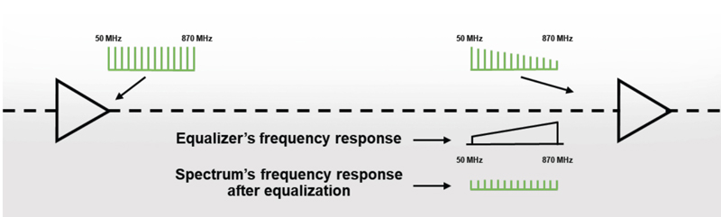
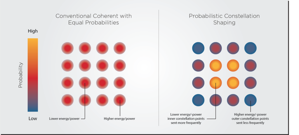


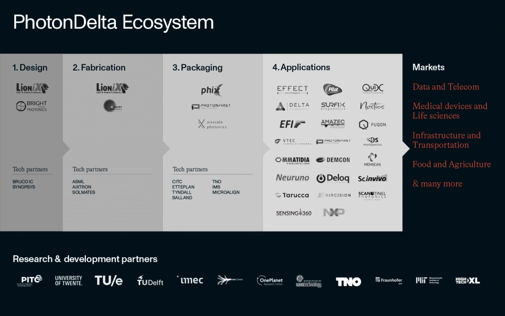
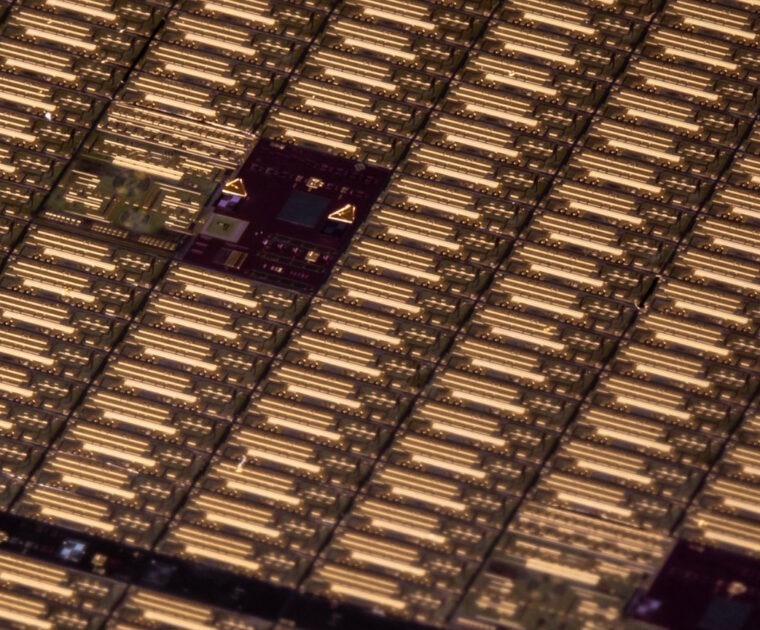


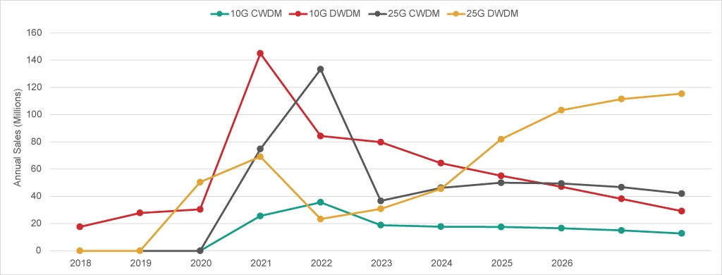
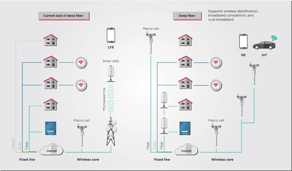

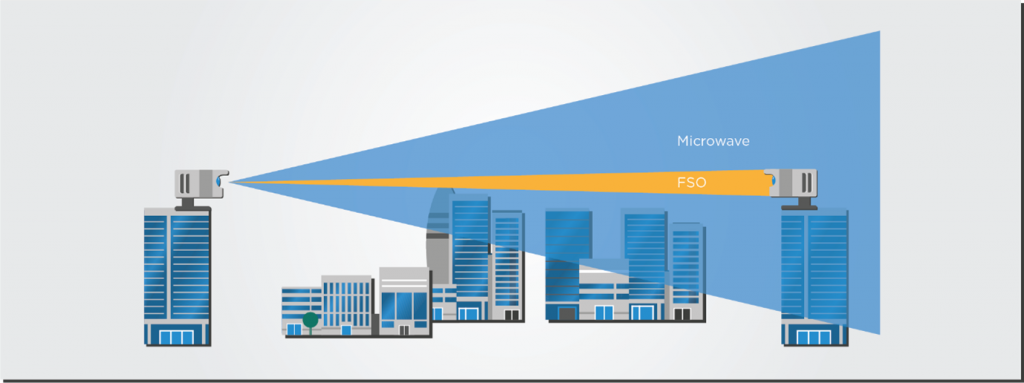
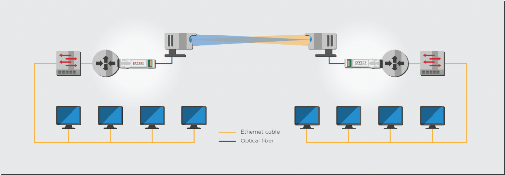

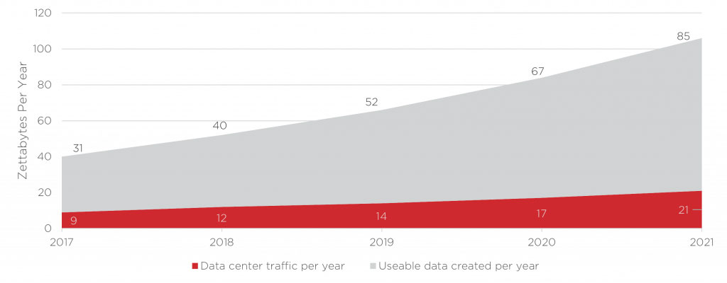
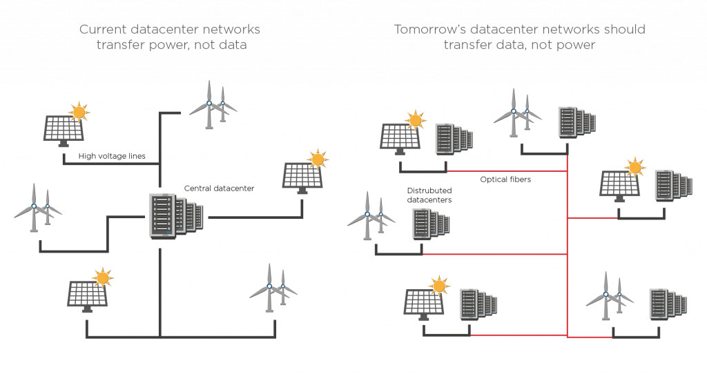


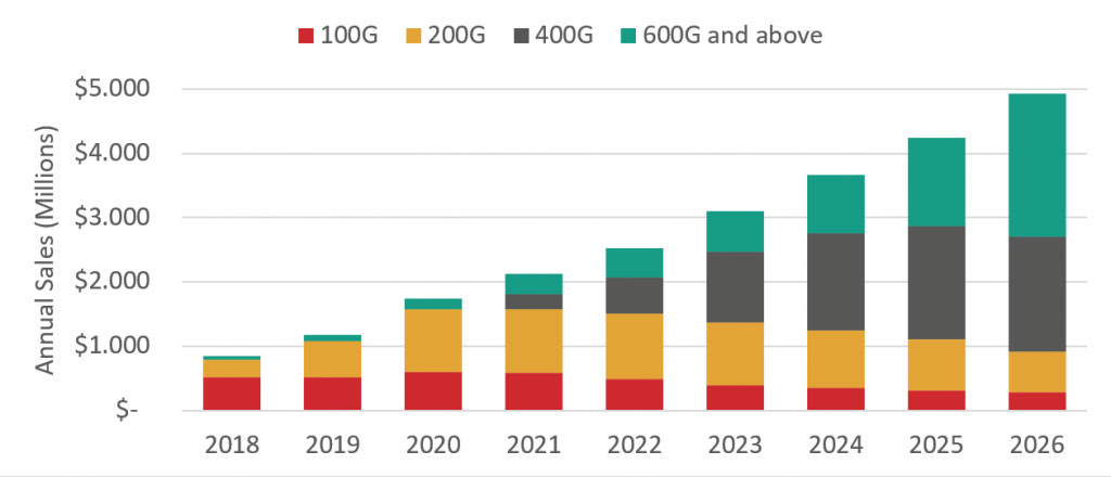
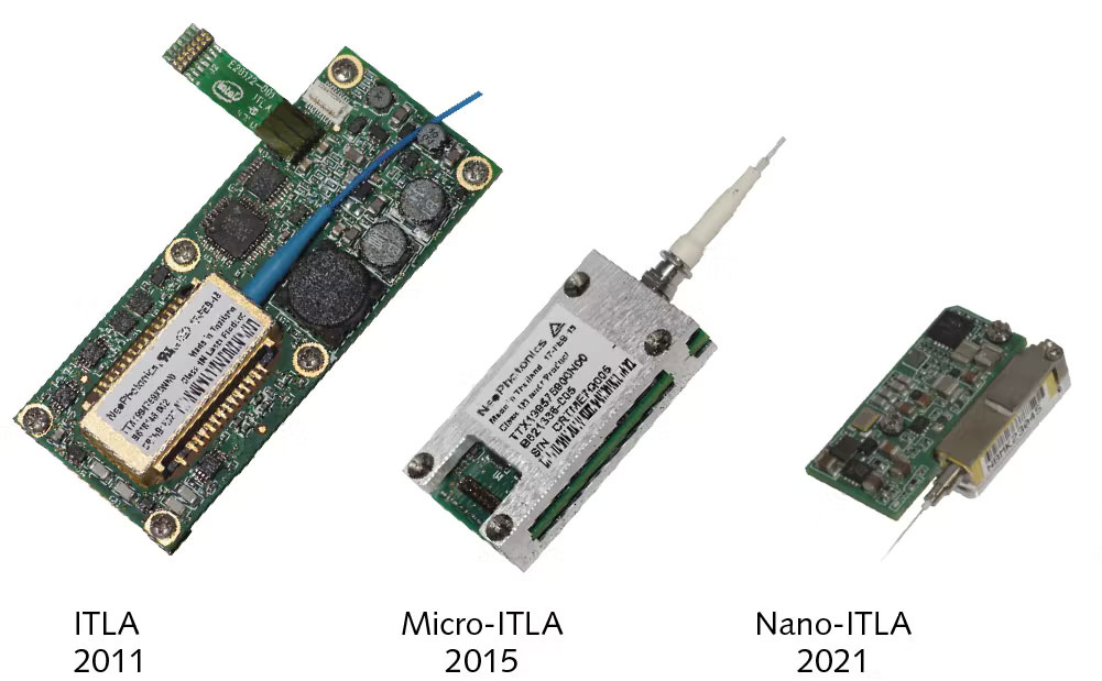
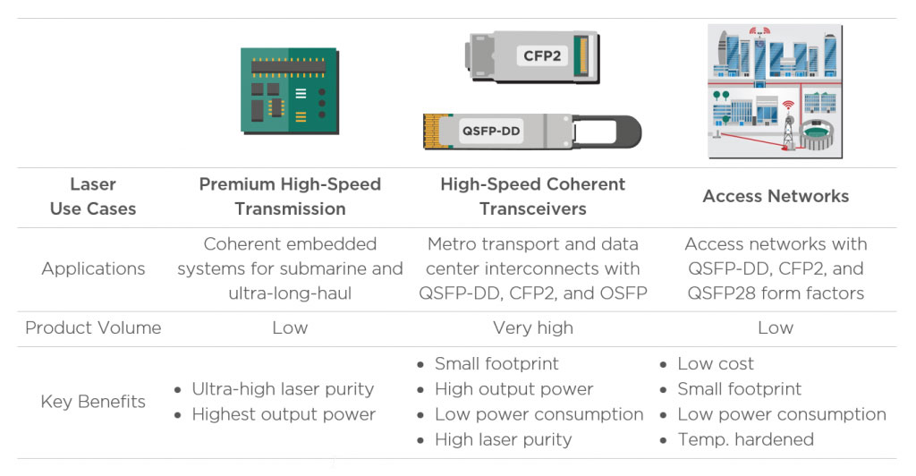
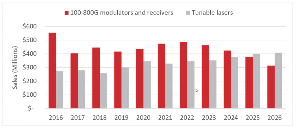
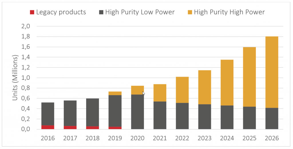

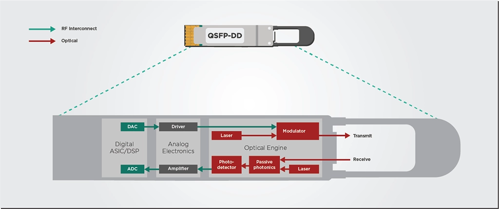
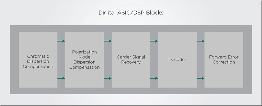


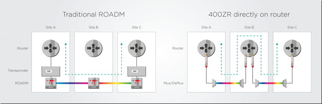
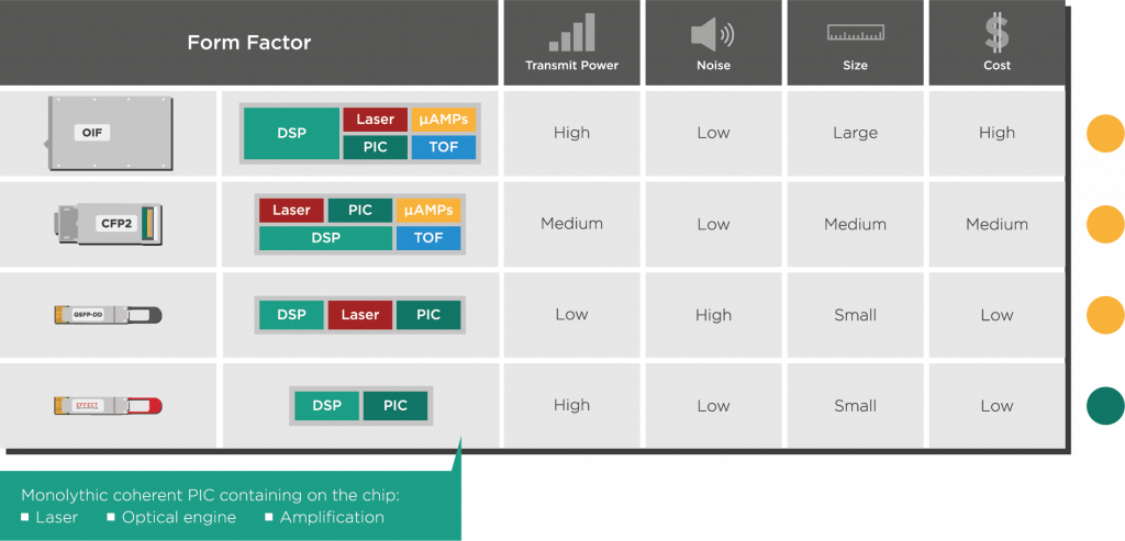

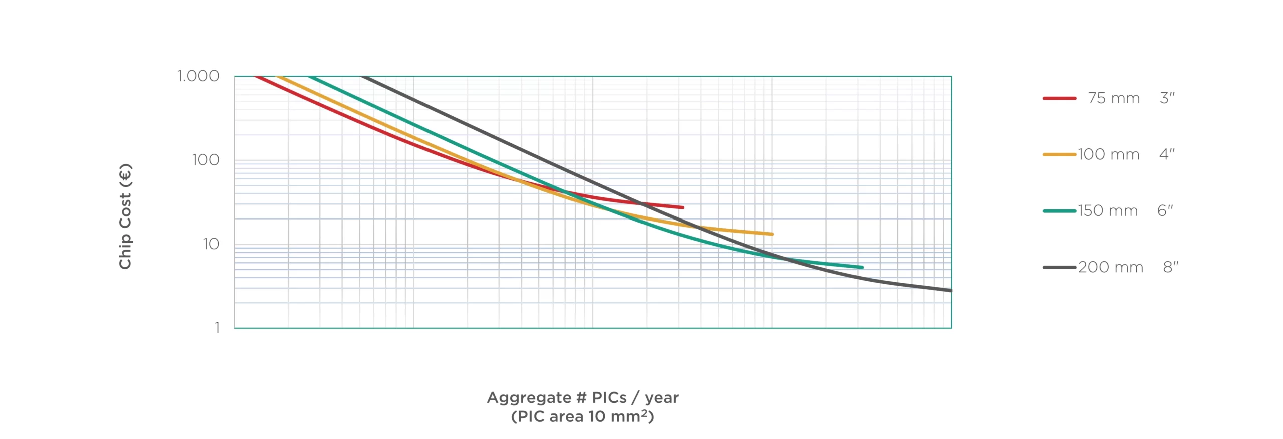

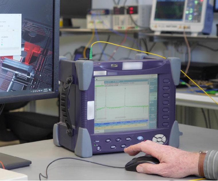


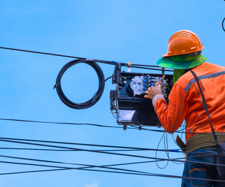
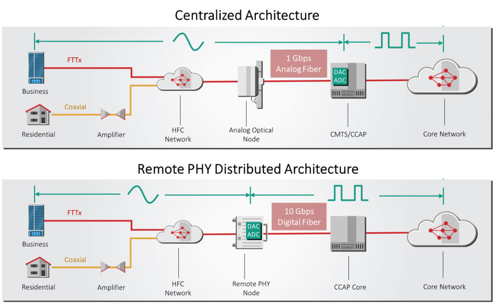
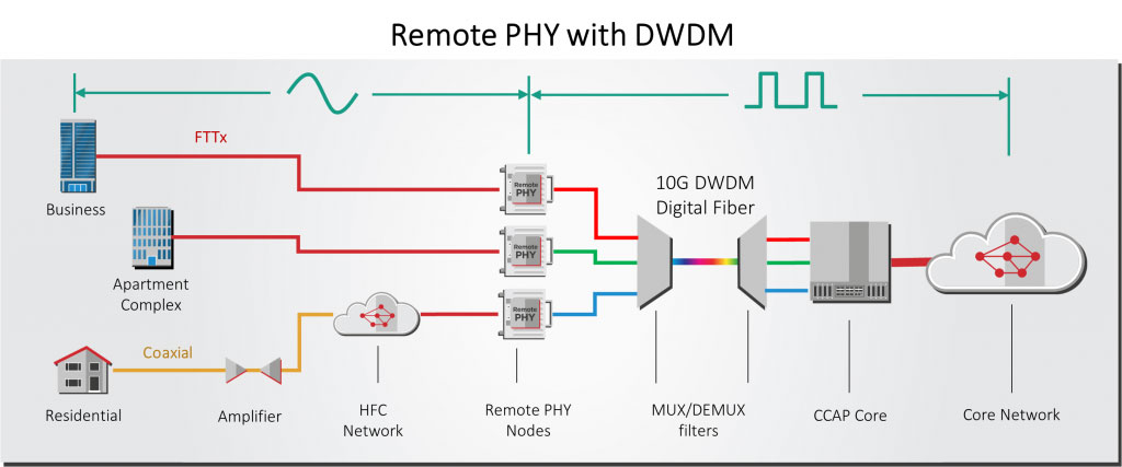
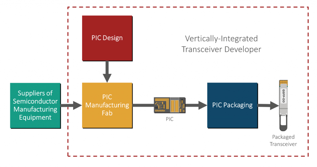
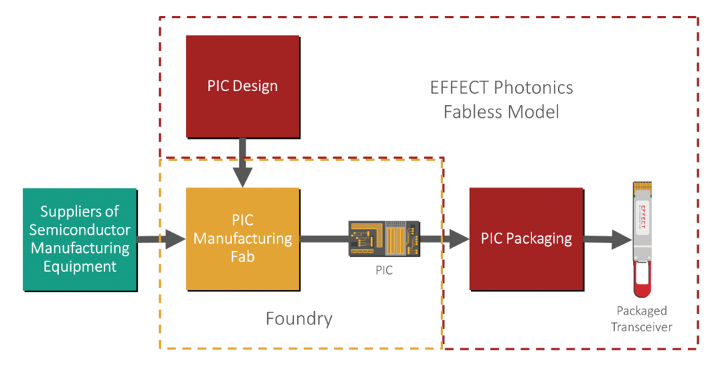


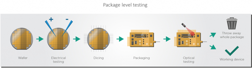
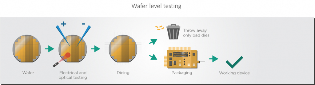


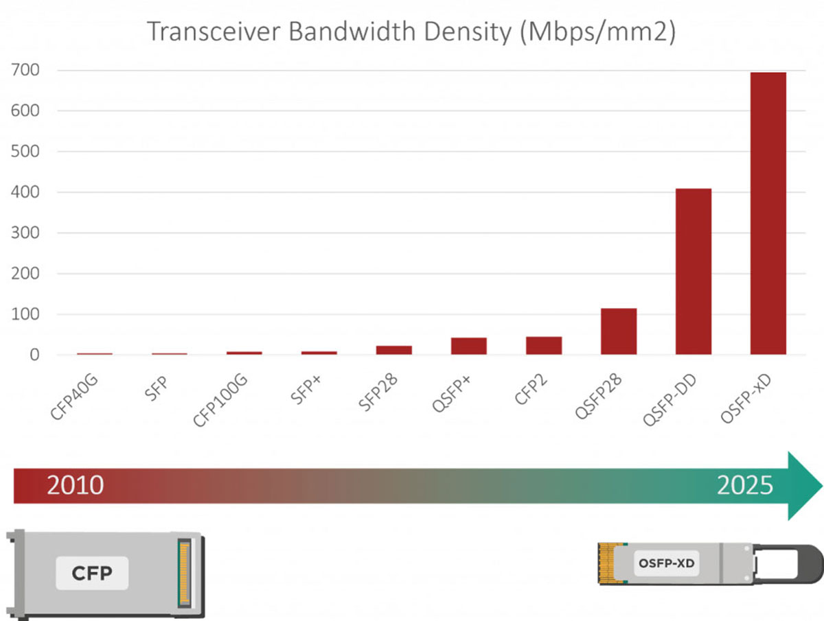
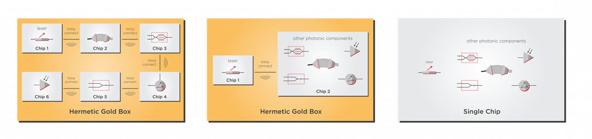


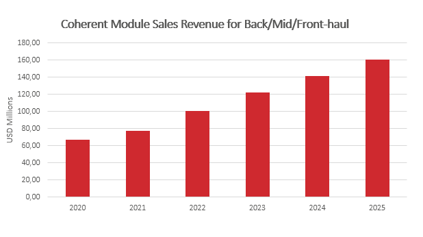
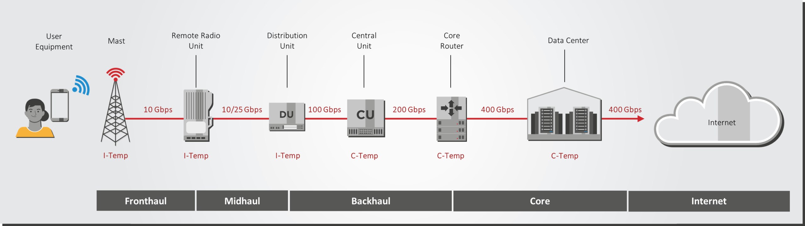


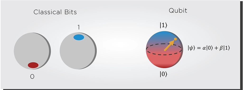
![Figure 2: Quantum computation as an interference process. The quantum circuit processes all the potential possibilities, canceling out the wrong solution and reinforcing the correct solution. [Source: Qiskit]](https://effectphotonics.com/wp-content/uploads/2024/01/Intro-into-QKD-Figure-2.webp)
![Figure 3: Example of a communications link encrypted via QKD. [Source: TU Eindhoven]](https://effectphotonics.com/wp-content/uploads/2024/01/Intro-into-QKD-Figure-1024x576.webp)


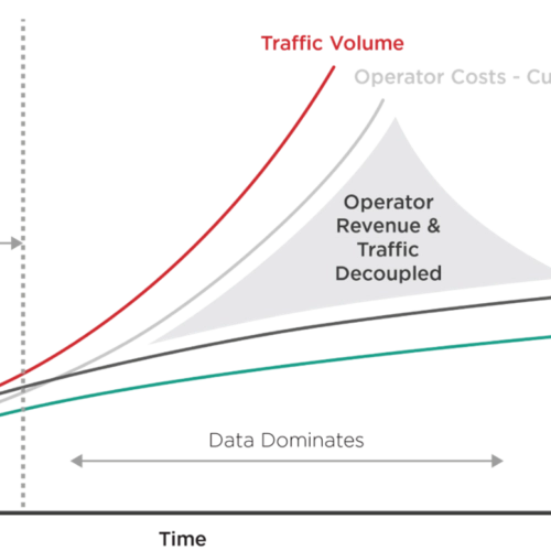


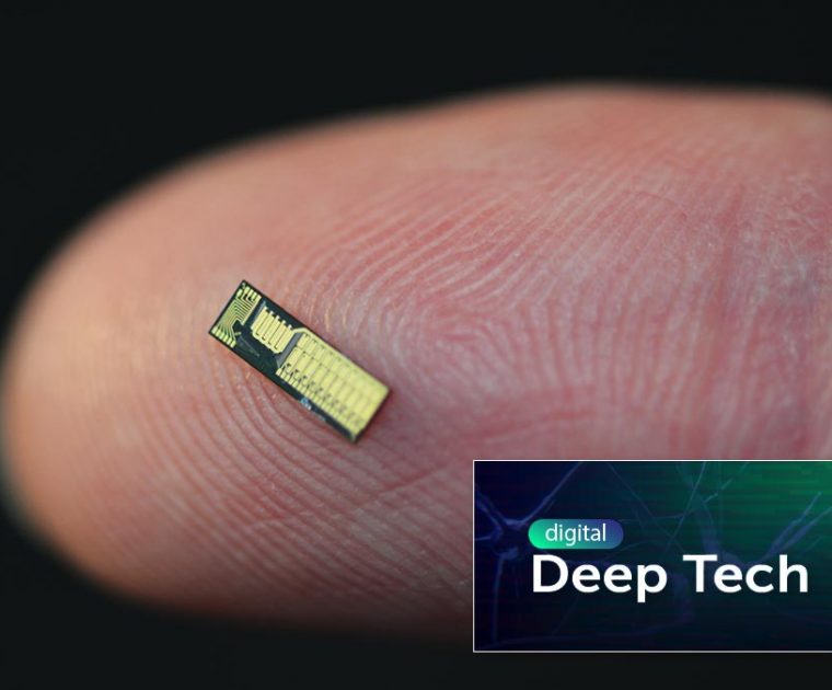


