
Designing a Coherent Transceiver
Coherent transmission has become a fundamental component of optical networks to address situations where direct detect technology cannot provide the required capacity and reach.
While direct detect transmission only uses the amplitude of the light signal, coherent optical transmission manipulates three different light properties: amplitude, phase, and polarization. These additional degrees of modulation allow for faster optical signals without compromising on transmission distance. Furthermore, coherent technology enables capacity upgrades without replacing the expensive physical fiber infrastructure in the ground.
Given its importance, in this article, we want to explain some key aspects of the design processes going on in transceivers.
Key Components of An Optical Transceiver
An optical transceiver has both electrical and optical subsystems, each with its specific components. Each component plays a crucial role in enabling high-speed, long-haul data transmission. Here are the primary components of a coherent optical transceiver:
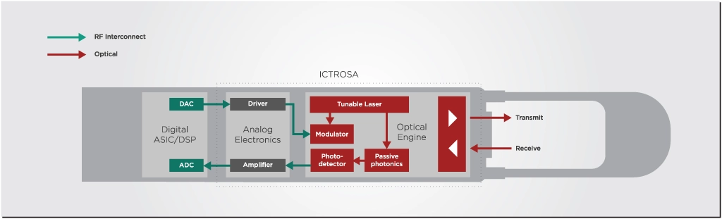
- Laser Source: The laser source generates the coherent light used for transmission. It determines many of the characteristics of the transmitted optical signal, from its wavelength and power to its noise tolerance. Read our previous article to know more about what goes inside laser design.
- Optical engine: The optical engine includes the modulator and receiver components as well as passive optical components required to guide, combine or split optical signals. The modulator encodes data onto the optical signal and the receiver converts the optical signal into an electrical signal. Depending on the material used (indium phosphide or silicon), the optical engine chip might also include the tunable laser.
- Digital/Analog Converters (DAC/ADC): The Digital-to-Analog Converter (DAC) turns digital signals from the digital processing circuitry into analog signals for modulation. The Analog-to-Digital Converter (ADC) does the reverse process.
- Digital Signal Processor (DSP): The DSP performs key signal processing functions, including dispersion compensation, polarization demultiplexing, carrier phase recovery, equalization, and error correction. Read this article to know more about what goes inside a DSP.
- Forward Error Correction (FEC) Encoder/Decoder: FEC is crucial for enhancing the reliability of data transmission by adding redundant bits that allow a receiver to check for errors without asking for retransmission of the data.
- Control and Monitoring Interfaces: Transceivers feature control and monitoring interfaces for managing and optimizing their operation.
- Power Management and Cooling Systems: These include heatsinks and thermoelectric coolers required to maintain the components within their specified temperature ranges and ensure reliable transceiver operation.
Key Design Processes in a Transceiver
Designing a transceiver is a process that should take an initial application concept into a functioning transceiver device that can be manufactured. It’s a complex, layered process that involves designing many individual components and subsystems separately but also predicting and simulating how all these components and subsystems will interact with each other.
Writing a faithful, nuanced summary of this design process is beyond the scope of this article, but we will mention in very broad terms some of the key processes going on.
- Defining Concept and Specifications: We must first define what goes into the transceiver and the expected performance. Transceiver architects will spend time with product management to understand the customer’s requirements and their impact on design choices. Some of these requirements and designs are already standardized, some of them (like EFFECT Photonics’ optical engine) are proprietary and will require deeper thinking in-house. After these conversations, the transceiver concept becomes a concrete set of specifications that are passed on to the different teams (some in-house, others from company partners).
- Optical Subsystem Design: The optical subsystem in the transceiver generates, manipulates, and receives the light signal. Optical designers develop a schematic circuit diagram that captures the function of the optical subsystem, which includes lasers, modulators, or light detectors. The designers will simulate the optical system to make sure it works, and then translate this functional design into an actual optical chip layout that can be manufactured at a semiconductor foundry.
- Electronic Subsystem Design: In parallel with the optical subsystem, the electronic subsystem is also being designed. The heart of the electronic subsystem is the DSP chip. The DSP design team also comes up with a functional model of the DSP and must simulate it and translate it into a layout that can be manufactured by a semiconductor foundry. However, there’s a lot more to the electronic system than just the DSP: there are analog-to-digital and digital-to-analog converters, amplifiers, drivers, and other electronic components required for signal conditioning. All of these components can be acquired from another vendor or designed in-house depending on the requirements and needs.
- Mechanical and Thermal Design: The mechanical and thermal design of the pluggable transceiver is essential to ensure its compatibility with industry-standard form factors and enable reliable operation. Mechanical considerations include connector types, physical dimensions, and mounting mechanisms. The thermal design focuses on heat dissipation and ensures the transceiver operates within acceptable temperature limits.
The Importance of a Co-Design Philosophy
Transceiver developers often source their DSP, laser, and optical engine from different suppliers, so all these chips are designed separately. This setup reduces the time to market and simplifies the research and design processes but comes with trade-offs in performance and power consumption.
A co-design approach that features strong interactions between the different teams that design these systems can lead to a much better fit and efficiency gains. You can learn more about the potential advantages of co-designing optical and electronic subsystems in this article.
Takeaways
In summary, designing a coherent optical pluggable transceiver involves carefully considering and balancing many different systems, standards, and requirements, from optical and electrical subsystems to mechanical and thermal design and component procurement. These design processes ensure the development of a reliable, high-performance optical transceiver that meets industry standards and fulfills the specific requirements of the target application.