
The Promise of Integrated Quantum Photonics
Today’s digital society depends heavily on securely transmitting and storing data. One of the oldest and most widely used methods to encrypt data is called RSA (Rivest-Shamir-Adleman – the surnames of the algorithm’s designers). However, in 1994 mathematician Peter Shor proved that an ideal quantum computer could find the prime factors of large numbers exponentially more quickly than a conventional computer and thus break RSA encryption within hours or days.
While practical quantum computers are likely decades away from implementing Shor’s algorithm with enough performance and scale to break RSA or similar encryption methods, the potential implications are terrifying for our digital society and our data safety.
Given these risks, arguably the most secure way to protect data and communications is by fighting quantum with quantum: protect your data from quantum computer hacking by using security protocols that harness the power of quantum physics laws. That’s what quantum key distribution (QKD) does.
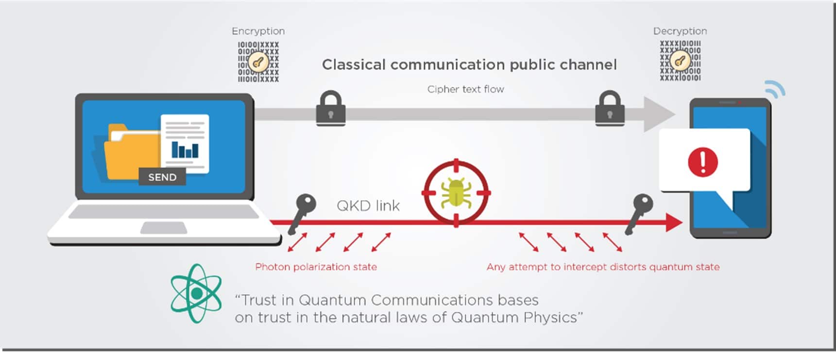
The quantum bits (qubits) used by QKD systems can be photons, electrons, atoms, or any other system that can exist in a quantum state. However, using photons as qubits will likely dominate the quantum communications and QKD application space. We have decades of experience manipulating the properties of photons, such as polarization and phase, to encode qubits. Thanks to optical fiber, we also know how to send photons over long distances with relatively little loss. Besides, optical fiber is already a fundamental component of modern telecommunication networks, so future quantum networks can run on that existing fiber infrastructure. All these signs point towards a new era of quantum photonics.
Photonic QKD devices have been, in some shape or form, commercially available for over 15 years. Still, factors such as the high cost, large size, and the inability to operate over longer distances have slowed their widespread adoption. Many R&D efforts regarding quantum photonics aim to address the size, weight, and power (SWaP) limitations. One way to overcome these limitations and reduce the cost per device would be to integrate every QKD function—generating, manipulating, and detecting photonic qubits—into a single chip.
Integration is Key to Bring Lab Technology into the Market
Bringing quantum products from lab prototypes to fully realized products that can be sold on the market is a complex process that involves several key steps.
One of the biggest challenges in bringing quantum products to market is scaling up the technology from lab prototypes to large-scale production. This requires the development of reliable manufacturing processes and supply chains that can produce high-quality quantum products at scale. Quantum products must be highly performant and reliable to meet the demands of commercial applications. This requires extensive testing and optimization to ensure that the product meets or exceeds the desired specifications.
In addition, quantum products must comply with relevant industry standards and regulations to ensure safety, interoperability, and compatibility with existing infrastructure. This requires close collaboration with regulatory bodies and industry organizations to develop appropriate standards and guidelines.
Photonic integration is a process that makes these goals more attainable for quantum technologies. By taking advantage of existing semiconductor manufacturing systems, quantum technologies can more scale up their production volumes more easily.
Smaller Footprints and Higher Efficiency
One of the most significant advantages of integrated photonics is its ability to miniaturize optical components and systems, making them much smaller, lighter, and more portable than traditional optical devices. This is achieved by leveraging micro- and nano-scale fabrication techniques to create optical components on a chip, which can then be integrated with other electronic and optical components to create a fully functional device.
The miniaturization of optical components and systems is essential for the development of practical quantum technologies, which require compact and portable devices that can be easily integrated into existing systems. For example, compact and portable quantum sensors can be used for medical imaging, geological exploration, and industrial process monitoring. Miniaturized quantum communication devices can be used to secure communication networks and enable secure communication between devices.
Integrated photonics also allows for the creation of complex optical circuits that can be easily integrated with other electronic components, to create fully integrated opto-electronic quantum systems. This is essential for the development of practical quantum computers, which require the integration of a large number of qubits (quantum bits) with control and readout electronics.
Economics of Scale
Wafer scale photonics manufacturing demands a higher upfront investment, but the resulting high-volume production line drives down the cost per device. This economy-of-scale principle is the same one behind electronics manufacturing, and the same must be applied to photonics. The more optical components we can integrate into a single chip, the more can the price of each component decrease. The more optical System-on-Chip (SoC) devices can go into a single wafer, the more can the price of each SoC decrease.
Researchers at the Technical University of Eindhoven and the JePPIX consortium have done some modelling to show how this economy of scale principle would apply to photonics. If production volumes can increase from a few thousands of chips per year to a few millions, the price per optical chip can decrease from thousands of Euros to mere tens of Euros. This must be the goal for the quantum photonics industry.
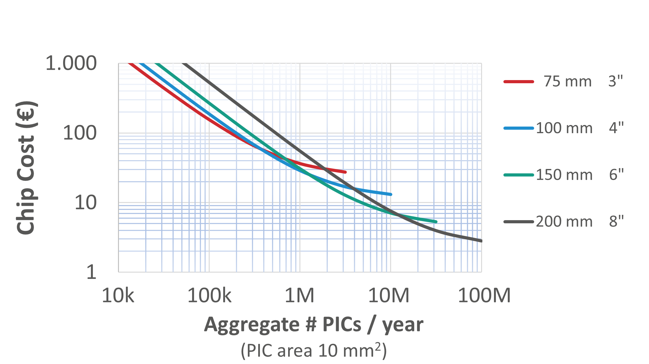
By integrating all optical components on a single chip, we also shift the complexity from the assembly process to the much more efficient and scalable semiconductor wafer process. Assembling and packaging a device by interconnecting multiple photonic chips increases assembly complexity and costs. On the other hand, combining and aligning optical components on a wafer at a high volume is much easier, which drives down the device’s cost.
Takeaways
Overall, bringing quantum products to market requires a multi-disciplinary approach that involves collaboration between scientists, engineers, designers, business professionals, and regulatory bodies to develop and commercialize a high-quality product that meets the needs of its target audience. Integrated photonics offers significant advantages in miniaturization and scale-up potential, which are essential in taking quantum technologies from the lab to the market.