
Making Smaller Lasers at a Big Scale
The world is moving towards tunability. The combination of tunable lasers and dense wavelength division multiplexing (DWDM) allows datacom and telecom industries to expand their network capacity without increasing their existing fiber infrastructure. Furthermore, the miniaturization of coherent technology into pluggable transceiver modules has finally enabled the widespread implementation of IP over DWDM solutions.
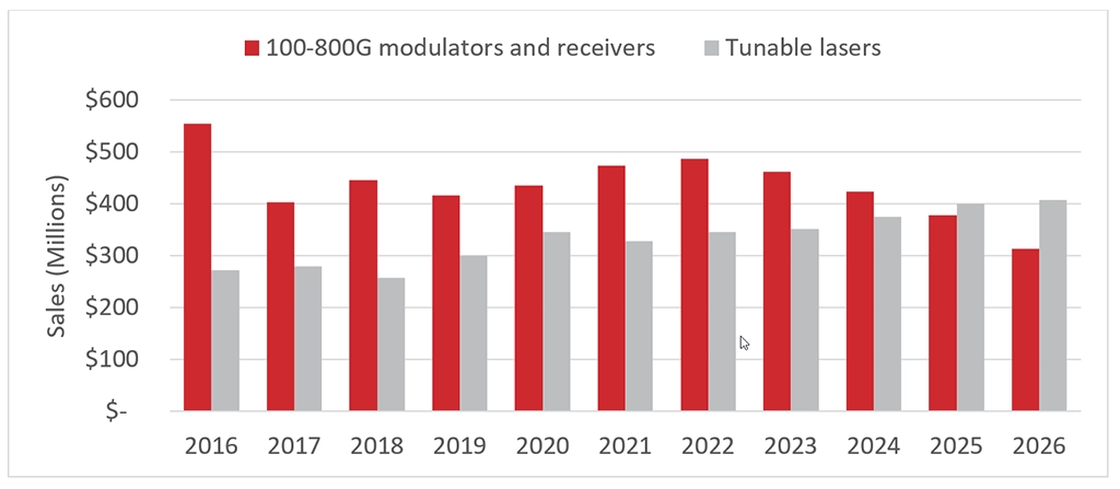
With the increasing demand for coherent transceivers, many companies have performed acquisitions and mergers that allow them to develop transceiver components internally and thus secure their supply. LightCounting forecasts show that while this consolidation will decrease the sales of modulator and receiver components, the demand for tunable lasers will continue to grow. The forecast expects the tunable laser market for the transceiver to reach a size of $400M in 2026.
East Asia is a huge driver of the rising number of tunable lasers sales. With initiatives like the “Broadband China” strategy and significant investments in 5G and beyond, the demand for advanced optical components, including tunable lasers, has surged in China. Japan and South Korea have a long history of adopting early new optical telecom innovations. After all, Japanese companies are at the forefront of research and development in tunable laser technology, and South Korea has built highly future-proofed 5G networks that are ahead of the implementations in Europe and North America. To meet the demands of this region, the industry needs to improve at making highly integrated tunable lasers at scale.
Making New and Smaller Lasers
The impact of small and integrated lasers extends beyond mere size considerations; it crucially contributes to enhancing power efficiency. Smaller laser designs inherently operate at lower voltages and currents, offering improved heat dissipation and minimizing coupling losses. Photonic integration helps achieve these reductions, maximizing efficiency by consolidating multiple functions onto a single chip.
The journey towards 100G coherent technology in access networks requires compact and power-efficient coherent pluggables in the QSFP28 form factor and, with it, compact and power-efficient tunable lasers that fit this form factor.
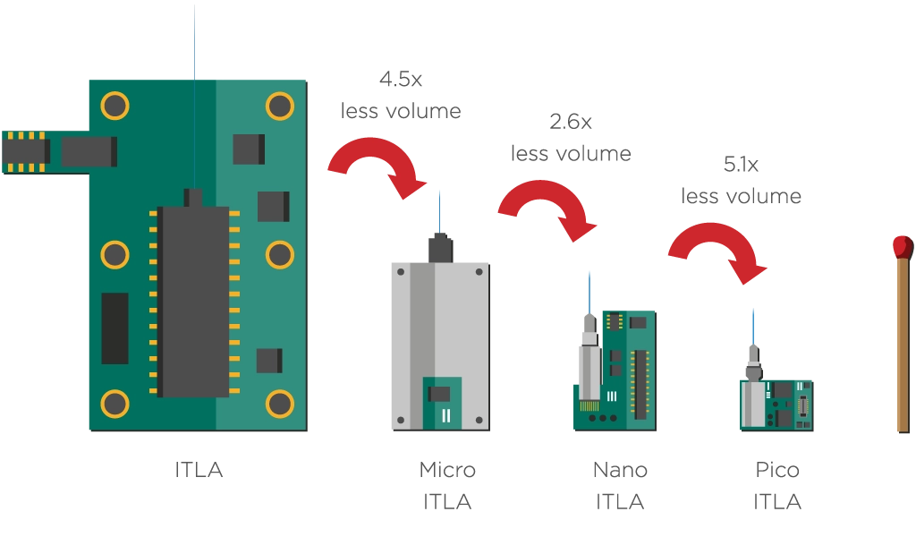
This monolithic integration of all tunable laser functions allowed EFFECT Photonics to develop a novel pico-ITLA (pITLA) module that will become the world’s smallest ITLA for coherent applications. The pITLA is the next step in tunable laser integration, including all laser functions in a package with just 20% of the volume of a nano-ITLA module. The figure below shows that even a standard matchstick dwarves the pITLA in size.
EFFECT Photonics’ laser solution is unique because it enables a widely tunable laser for which all its functions, including the wavelength locker, are monolithically integrated on a single chip. This setup is ideal for reducing power consumption and scaling into high production volumes.
The Economics of Scale
As innovative as these new, small lasers can be, they will have little impact if they cannot be manufactured at a high enough volume to satisfy the demands of mobile and cloud providers and drive down the cost per device.
This economy-of-scale principle is the same one behind electronics manufacturing, and the same must be applied to photonics. The more optical components we can integrate into a single chip, the more can the price of each component decrease. The more optical System-on-Chip (SoC) devices can go into a single wafer, the more can the price of each SoC decrease.
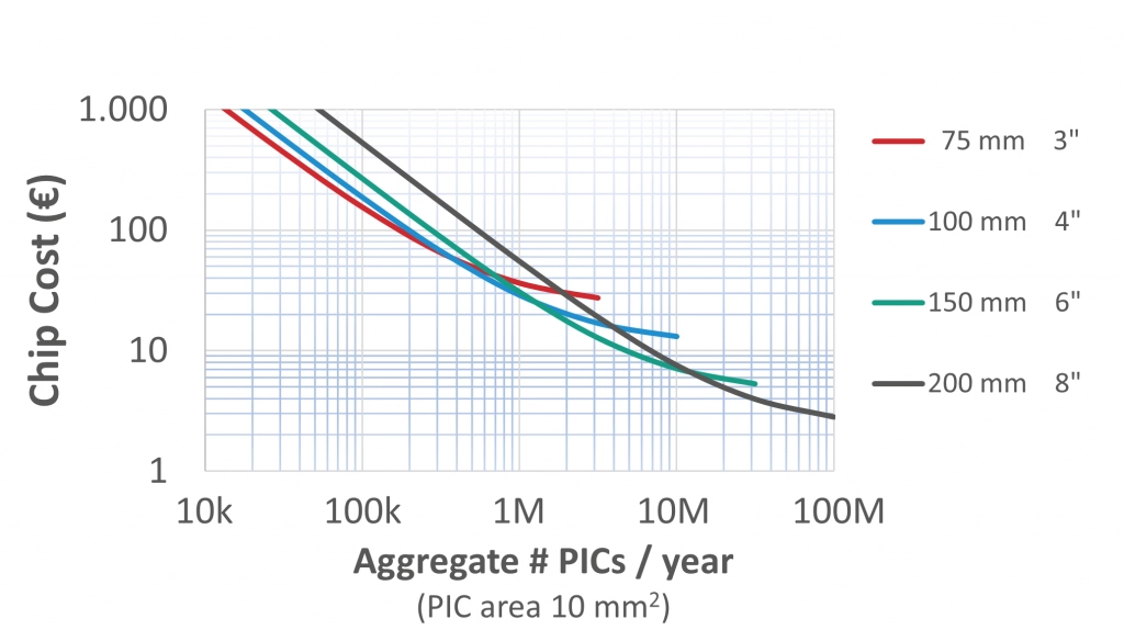
Researchers at the Technical University of Eindhoven and the JePPIX consortium have done some modelling to show how this economy of scale principle would apply to photonics. If production volumes can increase from a few thousands of chips per year to a few millions, the price per optical chip can decrease from thousands of Euros to mere tens of Euros. This must be the goal for the optical transceiver and tunable laser industry.
Learning to Scale from Electronics
A key way to improve photonics manufacturing is to learn from electronics packaging, assembly, and testing methods that are already well-known and standardized. After all, building a new special production line is much more expensive than modifying an existing production flow.
One electronic technique essential to transfer into photonics is ball-grid array (BGA) packaging. BGA-style packaging has grown popular among electronics manufacturers over the last few decades. It places the chip connections under the chip package, allowing more efficient use of space in circuit boards, a smaller package size, and better soldering.
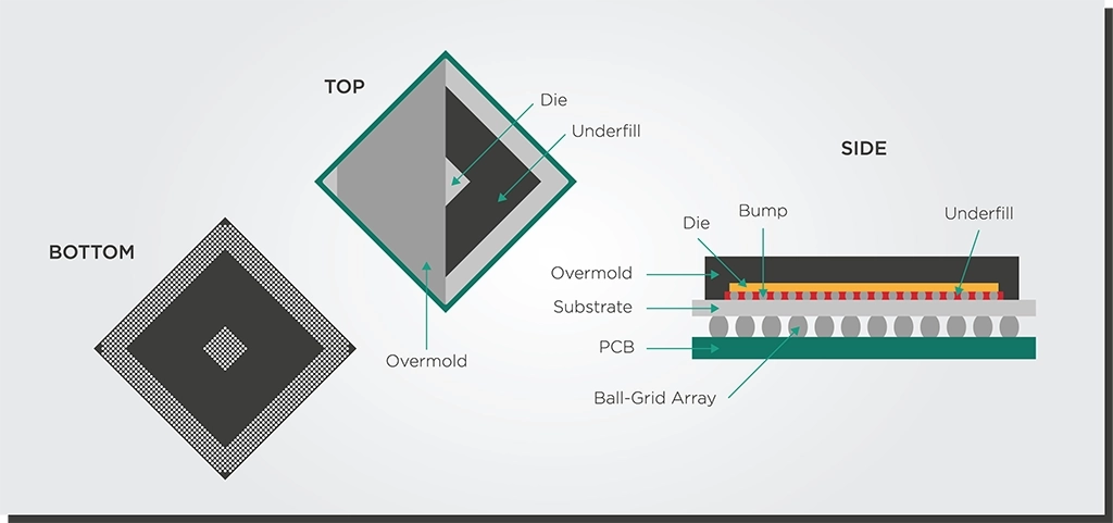
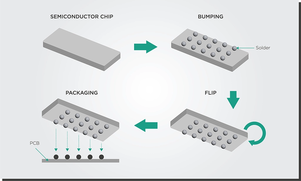
Another critical technique to move into photonics is flip-chip bonding. This process is where solder bumps are deposited on the chip in the final fabrication step. The chip is flipped over and aligned with a circuit board for easier soldering.
Takeaways
As the demand for data and telecommunication services surges globally, the industry is moving towards more compact, power-efficient, and scalable laser solutions that integrate all necessary functions on a single chip. With East Asia driving the demand for these advanced components through their ambitious broadband and 5G initiatives, the challenge now lies in applying the economies of scale principle from electronics manufacturing to photonics. This approach would dramatically reduce costs and enable the mass adoption of these technologies.