The optical transceiver market is expected to double in size by 2025, and coherent optical…
The optical transceiver market is expected to double in size by 2025, and coherent optical technology has come a long way over the past decade to become more accessible and thus have a greater impact on this market. When Nortel (later Ciena) introduced the first commercial coherent transponder in 2008, the device was a bulky, expensive line card with discrete components distributed on multiple circuit boards.
As time went by, coherent devices got smaller and consumed less power. By 2018, most coherent line card transponder functions could be miniaturized into CFP2 transceiver modules that were the size of a pack of cards and could plug into modules with pluggable line sides. QSFP modules followed a couple of years later, and they were essentially the size of a large USB stick and could be plugged directly into routers. They were a great fit for network operators who wanted to take advantage of the lower power consumption and cost, field replaceability, vendor interoperability, and pay-as-you-grow features.
Figure 1: Coherent module size and power consumption evolution from OIF MSA line card modules to pluggable modules like CFP and QSFP.
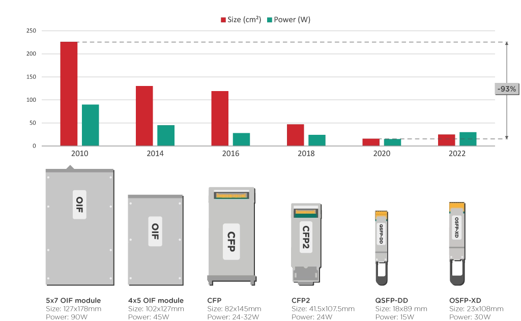
Despite the onset of pluggables, the big, proprietary line card optical engines have still played a role in the market by focusing on delivering best-in-class optical performance. The low-noise, high-power signals they produce have the longest reach for optical links and have wider compatibility with the ROADM multiplexers used in metro and long-haul networks. The smaller CFP2 modules produce at best roughly half the laser power of the line card modules, which limits their reach. Meanwhile, even smaller QSFP form factors can not fit optical amplifier components, so their transmit power and reach is much more limited than even a CFP2 module.
All in all, the trade-offs were clear: go for proprietary line card transponders if you want best-in-class performance and longest reach, and go for CFP2 or QSFP transceivers if you want a smaller footprint and power consumption. This trade-off, however, limits the more widespread adoption of coherent technology. For example, mobile network operators need high-performance but also smaller footprint and power consumption so that their metro and access networks can meet the rising demands for 5G data.
So what if we told you the current paradigm of line card transponders versus pluggable transceivers is outdated? Recent improvements in electronic and photonic integration have squeezed more performance and functions into smaller form-factors, allowing pluggable devices to almost catch up to line cards. A transceiver that offers both high-end performance and reach as well as small footprint and power consumption can have a disruptive impact on this growing transceiver market. Developing such a device would exploit a valuable market opportunity.
Integration enables line card performance in a pluggable format
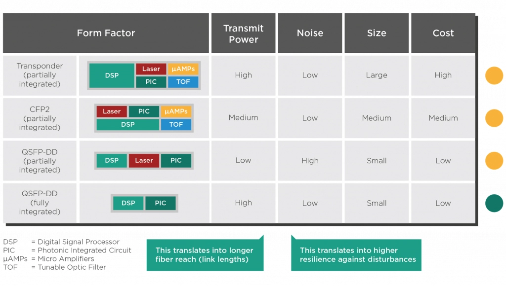
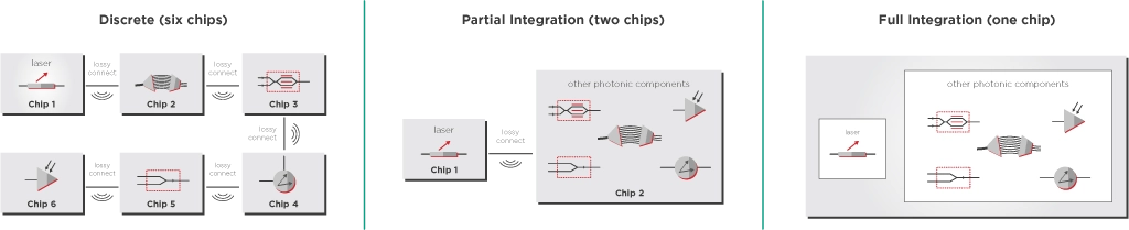
The advances in photonic integration change the game and can enable high performance and transmit power in the smallest pluggable transceiver form factors. By integrating all photonic functions on a single chip, including lasers and optical amplifiers, EFFECT Photonics’ pluggable transceiver modules can achieve transmit power levels similar to those of line card transponder modules while still keeping the smaller QSFP router pluggable form factor, power consumption, and cost.
Figure 2: Comparing transmit power, noise, size, and cost of line card transponders and different transceiver pluggable modules. Fully integrated QSFP-DD modules include lasers, amplifiers, and filters inside a single PIC, so they can deliver high transmit powers at small size and low cost.
Our full integration technology increases the transmit power by minimizing the optical losses due to the use of more efficient optical modulators, fewer material losses compared to silicon, and the integration of the laser device on the same chip as the rest of the optical components. Line card transponders are still the best bet to reach the highest performance level of 800G and beyond as well as implement non-standard constellation schemes. However, for many other use cases pluggable modules can already match the performance of line card transponders.
Modern ASICs can fit electronic functions in a pluggable form factor
As important as optical performance is, though, pluggable transceivers also needed improvements on the electronic side.
Traditionally, line card systems not only had better optical performance but also broader and more advanced electronic functionalities, such as digital signal processing (DSP), advanced forward error correction (FEC), encryption, and advanced modulation schemes. These features are usually implemented on electronic application-specific integrated circuits (ASICs).
ASICs benefit from the same CMOS process improvements that drive progress in consumer electronics. Each new CMOS process generation can fit more transistors into a single chip. Ten years ago, an ASIC for line cards had tens of millions of transistors, while the 7nm ASIC technology used in modern pluggables has more than five billion transistors. This progress in transistor density allows ASICs to integrate more electronic functions than ever into a single chip while still making the chip smaller. Previously, every function—signal processing, analog/digital conversion, error correction, multiplexing, encryption—required a separate ASIC, but now they can all be consolidated on a single chip that fits in a pluggable transceiver.
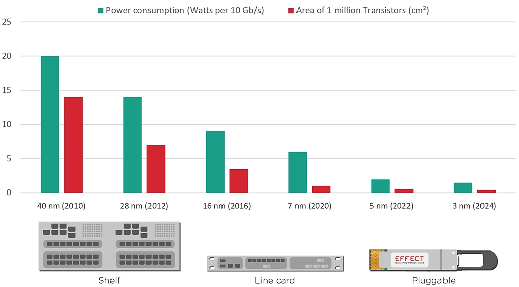
This increase in transistor density and integration also leads to massive gains in power consumption and performance. For example, modern transceivers using 7nm ASICs have decreased their consumption by 50% compared to the previous generation using 16nm ASICs while delivering roughly a 30% increase in bandwidth and baud rates. By 2022, ASICs in pluggables will benefit from a newer 5nm CMOS process, enabling further improvements in transistor density, power consumption, and speed.
Electronic integration enables line card system management in a pluggable form factor
The advancements in CMOS technology also enable the integration of system-level functions into a pluggable transceiver. Previously, functions such as in-band network management and security, remote management, autotuneability, or topology awareness had to live on the shelf controller or in the line card interface, but that’s not the case anymore. Thanks to the advances in electronic integration, we are closer than ever to achieving a full, open transponder on a pluggable that operates as part of the optical network. These programmable, pluggable transceivers provide more flexibility than ever to manage access networks.
For example, the pluggable transceiver could run in a mode that prioritizes high-performance or one that prioritizes low consumption by using simpler and less power-hungry signal processing and error correction features. Therefore, these pluggables could provide high-end performance in the smallest form-factor or low and mid-range performance at lower power consumption than embedded line card transponders.
EFFECT Photonics has already started implementing these kinds of system-management features in its product. For example, our direct-detect SFP+ transceiver modules feature NarroWave technology that allows customers to monitor and control remote SFP+ modules from the central office without making any hardware or software changes in the field. NarroWave is agnostic of vendor equipment, data rate, or protocol of the in-band traffic.
Pluggable transceivers also provide the flexibility of multi-vendor interoperability. High-performance line card transponders have often prioritized the use of proprietary features to increase performance while neglecting interoperability. The new generations of pluggables don’t need to make this trade off: they can operate in standards-compatible modes for interoperability or in high-performance modes that use proprietary features.
Takeaways
Coherent technology was originally reserved for premium long-distance links where performance is everything. Edge and access networks could not use this higher-performance technology since it was too bulky and expensive.
Photonic integration technology like the one used by EFFECT Photonics helps bring these big, proprietary, and expensive line card systems into a router pluggable form factor. This tech has squeezed more performance into a smaller area and at lower power consumption, making the device more cost-effective. Combining the improvements in photonic integration with the advances in electronic integration for ASICs, the goal of having a fully programmable transponder in a pluggable is practically a reality. Photonic integration will be a disruptive technology that will simplify network design and operation and reduce network operators’ capital and operating expenses.
The impact of this technological improvement in pluggable transceivers was summarized deftly by Keven Wollenweber, VP of Product Management for Cisco’s Routing Portfolio: “Technology advancements have reached a point where coherent pluggables match the QSFP-DD form factor of grey optics, enabling a change in the way our customers build networks. 100G edge and access optimized coherent pluggables will not only provide operational simplicity, but also scalability, making access networks more future proof.”
If you would like to download this article as a PDF, then please click here. Tags: 100G, access network, ASIC, CFP, coherent optics, CoherentPIC, DSP, edge network, electronic integration, fully integrated, Fully Integrated PICs, Integrated Photonics, line card, metro access, miniaturization, NarroWave, optical transceivers, photonic integration, PIC, pluggable, pluggable transceiver, QSFP, SFP+, small form factor, sustainability telecommunication
The World Needs Greener Telecommunications The demand for data and other digital services is rising…
The World Needs Greener Telecommunications
The demand for data and other digital services is rising exponentially. From 2010 to 2020, the number of Internet users worldwide doubled, and global internet traffic increased 12-fold. By 2022, internet traffic will likely double yet again. Mobile wireless networks will significantly drive this energy consumption upwards despite 5G being the most energy-aware mobile communication standard ever released. In a March 2020 report, Ericsson states that some communications service providers have estimated doubling their energy consumption to meet the increasing traffic demands after rolling out 5G.
Keeping up with the increasing data demand of future networks in a sustainable way will require operators to deploy more optical technologies, such as photonic integrated circuits (PICs), in their access and fronthaul networks. By replacing the inefficient copper and coaxial links that use electrical signals, operators can provide their customers and mobile sites with more data while reducing the required power per bit.
Integration Impacts Energy Efficiency and Optical Losses
Lately, we have seen many efforts to increase further the integration on a component level across the electronics industry. For example, moving towards greater integration of components in a single chip has yielded significant efficiency benefits in electronics processors. Apple’s M1 processor integrates all electronic functions in a single system-on-chip (SoC) and consumes a third of the power compared to the processors with discrete components used in their previous generations of computers.
Table 1: Comparing the power consumption of a Mac Mini with an M1 SoC chip to previous generations of Mac Minis. [Source: Apple’s website]
Photonics is also achieving greater efficiency gains by following a similar approach to integration. The more active and passive optical components (lasers, modulators, detectors, etc.) manufacturers can integrate on a single chip, the more energy they can save since they avoid coupling losses between discrete components and allow for interactive optimization.
Transceiver manufacturers have three choices in terms of design:
Discrete build – The transceiver components are manufactured through separate processes. The components are then assembled into a single package using different types of interconnections.
Partial integration – Some components are manufactured and integrated on the same chip, but others are manufactured or sourced separately. For example, the transceiver laser can be manufactured separately on a different material and then interconnected to a chip with the other transceiver components.
Full integration – All the components are manufactured on a single chip from a single material simultaneously.
While discrete builds and partial integration have advantages in managing the yield of the individual components, full integration has fewer losses and more efficient packaging and testing processes, making them a much better fit in terms of sustainability.
The interconnects required to couple discrete components result in electrical and optical losses that must be compensated with higher transmitter power and more energy consumption. The more interconnects between different components, the higher the losses become. Discrete builds will have the most interconnect points and highest losses. Partial integration reduces the number of interconnect points and losses compared to discrete builds. If these components are made from different optical materials, the interconnections will suffer additional losses.
On the other hand, full integration uses a single chip of the same base material. It does not require lossy interconnections between chips, minimizing optical losses and significantly reducing the energy consumption and footprint of the transceiver device.
Figure 1: Example of integrating a laser to other photonic components through different integration approaches.
More Integration Saves Scarce Resources
When it comes to energy consumption and sustainability, we shouldn’t just think about the energy the PIC consumes but also the energy and carbon footprint of fabricating the chip and assembling the transceiver. To give an example from the electronics sector, a Harvard and Facebook study estimated that for Apple, manufacturing accounts for 74% of their carbon emissions, with integrated circuit manufacturing comprising roughly 33% of Apple’s carbon output. That’s higher than the emissions from product use.
Figure 2: Apple’s carbon-emission breakdown. Manufacturing accounts for 74% of total emissions, and hardware use accounts for 19%. Carbon output from manufacturing integrated circuits (i.e., SoCs, DRAM, and NAND flash memory) is higher than that of hardware use. [Source: https://doi.org/10.1109/HPCA51647.2021.00076]
Chip manufacturing processes consume an immense amount of resources. A typical electronics semiconductor chip fab uses between 2 and 4 million gallons of water per day (that’s roughly between 7 and 15 million liters of water per day). Chips often need rare metals such as gold, cobalt, and silver or rare earth such as erbium yttrium, neodymium, or thulium. Mining and processing these materials are among the activities that produce the most waste and damage to the environment. To make things worse, we only recycle a small fraction of these materials. For example, the Global Enabling Sustainability Initiative estimates that high-tech products use 320 tons of gold every year and that less than 15% of the gold in e-waste is recovered for reuse.
The choice of integration approach has implications on the complexity of fabrication and packaging of the transceivers, which in turn has implications on their level of sustainability. For example, discrete integration requires a hermetically sealed gold box package to protect the interconnections from moisture. This packaging process also consumes more energy to create an airtight seal and consumes rare gold material. Partial integration reduces the number of interconnects and requires a smaller gold box, which reduces the cost and complexity of the packaging. However, this approach still requires separate fabrication processes for its components and interconnects, which increases the energy consumption of the assembly process. On the other hand, fully integrated transceivers can do away with the gold box and minimize energy consumption by avoiding the extra fabrication and packaging steps.
Early Testing Avoids Wastage
Testing is another aspect of the manufacturing process that impacts sustainability. The earlier faults can be found in the testing process, the greater the impact on the use of materials and the energy used to process defective chips. Ideally, testing should happen not only on the final, packaged transceiver but in the earlier stages of PIC fabrication, such as measuring after wafer processing or cutting the wafer into smaller dies.
Figure 3: Package vs. die level testing. Manufacturers can find faults earlier by testing at the die level, which avoids wasting packaging materials.
Discrete and partial integration approaches do more of their optical testing on the finalized package, after connecting all the different components together. Should just one of the components not pass the testing process, the complete packaged transceiver would need to be discarded, potentially leading to a massive waste of materials as nothing can be ”fixed” or reused at this stage of the manufacturing process.
Full integration enables earlier optical testing on the semiconductor wafer and dies. By testing the dies and wafers directly before packaging, manufacturers need only discard the bad dies rather than the whole package, which saves valuable energy and materials.
For example, EFFECT Photonics reaps these benefits in its production processes. 100% of electrical testing on the PICs happens at the wafer level, and our unique integration technology allows for 90% of optical testing to also happen on the wafer.
Full Integration Drives Sustainability
While communication networks have become more energy-efficient, further technological improvements must continue decreasing the cost of energy per bit and keeping up with the exponential increase in Internet traffic. At the same time, a greater focus is being placed on the importance of sustainability and responsible manufacturing. All the photonic integration approaches we have touched on will play a role in reducing the energy consumption of future networks. However, out of all of them, only full integration is in a position to make a significant contribution to the goals of sustainability and environmentally friendly manufacturing. A fully integrated system-on-chip minimizes optical losses, transceiver energy consumption, power usage, and materials wastage while at the same time ensuring increased energy efficiency of the manufacturing, packaging, and testing process.
If you would like to download this article as a PDF, then please click here.
EFFECT Photonics, a leading developer of high-performance dense wavelength division multiplexing (DWDM) optical components based…
EFFECT Photonics, a leading developer of high-performance dense wavelength division multiplexing (DWDM) optical components based on its optical System-on-Chip technology, will be exhibiting from February 17-18 2021 at the Photonics+ Virtual Exhibition and Conference, Feb 17-18, 2021. Photonics+ is a new networking event for the photonics industry and is arranged in partnership with EPIC (European Photonics Industry Consortium).
Join us with your colleagues, peers and over 250 international exhibitors and top speakers from the photonics industry at the Photonics+ event. The event consists of two afternoons for networking, business, sharing ideas, learning, and discussing new trends. With more than 5000 online visitors expected, a special AI enabled matchmaking function helps everyone find the right people and the right companies to get the most out of this major event.
The virtual exhibition hall works in a similar way to a physical exhibition. Browse the event hall and visit our virtual booth, watch our video, and download content such as product briefs and technical articles, schedule a meeting with a member of the EFFECT Photonics Team, and watch the EFFECT Photonics CTO Tim Koene give a presentation on “High-volume InP Photonic Integrated Circuits for Telecom and Sensing”.
EFFECT Photonics in a nutshell
Addressing the global need for higher bandwidth at affordable costs to end consumers, optical transceiver module solutions for modern telecommunication networks play a vital role. EFFECT Photonics has developed an InP (Indium Phosphide) photonics based System-on-Chip (SoC) technology to provide a new generation of flexible, and due to its extremely low power consumption, green and sustainable solutions for the market. By integrating ALL functions of an optical transceiver system onto a single photonic integrated chip (PIC), utilizing a unique in-house developed non-hermetic packaging technology, which removes the need for expensive hermetic (“gold box”) packaging, and combining it with scalable 3” and 4” wafer manufacturing, EFFECT Photonics is able to produce DWDM direct detect and coherent transceivers very cost-effectively. Because of this unique approach, EFFECT Photonics has established itself firmly to the forefront of high-tech photonics industry, serving both the telecom and sensing markets.
EFFECT Photonics has a production facility in Torbay (Brixham), UK. Torbay has a long tradition in the area of high-quality precision manufacturing and a strong photonics ecosystem which has been built over the last 50 years. At the Brixham facility, EFFECT Photonics is dedicated in developing and testing of packaging methods and is also one of the production facilities of the company.
With headquarters in Eindhoven, The Netherlands, EFFECT Photonics is an integral part of the European photonics research community. EFFECT Photonics is a member of the PhotonDelta Flagship Project. PhotonDelta is a growing ecosystem in Europe that covers a network of companies and knowledge institutes that intensively co-operates for the last 25 years in the research, design, development and manufacturing of integrated photonics technologies and components.