
Building a Sustainable Future with Fully Integrated PICs
Article first published 27 September 2021, updated 31st May 2023.
The demand for data and other digital services is rising exponentially. From 2010 to 2020, the number of Internet users worldwide doubled, and global internet traffic increased 12-fold. By 2022, internet traffic had doubled yet again. While 5G standards are more energy-efficient per bit than 4G, the total power consumption will be much higher than 4G. Huawei expects that the maximum power consumption of one of their 5G base stations will be 68% higher than their 4G stations. These issues do not just affect the environment but also the bottom lines of communications companies.
Keeping up with the increasing data demand of future networks sustainably will require operators to deploy more optical technologies, such as photonic integrated circuits (PICs), in their access and fronthaul networks.
Integration Impacts Energy Efficiency and Optical Losses
Lately, we have seen many efforts to increase further the integration on a component level across the electronics industry. For example, moving towards greater integration of components in a single chip has yielded significant efficiency benefits in electronics processors. Apple’s recent M1 and M2 processors integrate all electronic functions in a single system-on-chip (SoC) and consume significantly less power than the processors with discrete components used in their previous generations of computers.
| 𝗠𝗮𝗰 𝗠𝗶𝗻𝗶 𝗠𝗼𝗱𝗲𝗹 | 𝗣𝗼𝘄𝗲𝗿 𝗖𝗼𝗻𝘀𝘂𝗺𝗽𝘁𝗶𝗼𝗻 | |
| 𝗜𝗱𝗹𝗲 | 𝗠𝗮𝘅 | |
| 2023, M2 | 7 | 5 |
| 2020, M1 | 7 | 39 |
| 2018, Core i7 | 20 | 122 |
| 2014, Core i5 | 6 | 85 |
| 2010, Core 2 Duo | 10 | 85 |
| 2006, Core Solo or Duo | 23 | 110 |
| 2005, PowerPC G4 | 32 | 85 |
| Table 1: Comparing the power consumption of a Mac Mini with an M1 and M2 SoC chips to previous generations of Mac Minis. [Source: Apple’s website] | ||
Photonics is also achieving greater efficiency gains by following a similar approach to integration. The more active and passive optical components (lasers, modulators, detectors, etc.) manufacturers can integrate on a single chip, the more energy they can save since they avoid coupling losses between discrete components and allow for interactive optimization.
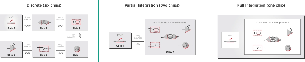
Let’s start by discussing three different levels of device integration for an optical device like a transceiver:
- Discrete build – The transceiver components are manufactured through separate processes. The components are then assembled into a single package using different types of interconnections.
- Partial integration – Some components are manufactured and integrated on the same chip, but others are manufactured or sourced separately. For example, the transceiver laser can be manufactured separately on a different material and then interconnected to a chip with the other transceiver components.
- Full integration – All the components are manufactured on a single chip from a single material simultaneously.
While discrete builds and partial integration have advantages in managing the production yield of the individual components, full integration leads to fewer optical losses and more efficient packaging and testing processes, making them a much better fit in terms of sustainability.
The interconnects required to couple discrete components result in electrical and optical losses that must be compensated with higher transmitter power and more energy consumption. The more interconnects between different components, the higher the losses become. Discrete builds will have the most interconnect points and highest losses. Partial integration reduces the number of interconnect points and losses compared to discrete builds. If these components are made from different optical materials, the interconnections will suffer additional losses.
On the other hand, full integration uses a single chip of the same base material. It does not require lossy interconnections between chips, minimizing optical losses and significantly reducing the energy consumption and footprint of the transceiver device.
More Integration Saves Scarce Resources
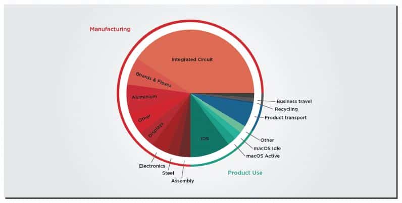
When it comes to energy consumption and sustainability, we shouldn’t just think about the energy the PIC consumes but also the energy and carbon footprint of fabricating the chip and assembling the transceiver. To give an example from the electronics sector, a Harvard and Facebook study estimated that for Apple, manufacturing accounts for 74% of their carbon emissions, with integrated circuit manufacturing comprising roughly 33% of Apple’s carbon output. That’s higher than the emissions from product use.
Early Testing Avoids Wastage
Testing is another aspect of the manufacturing process that impacts sustainability. The earlier faults can be found in the testing process, the greater the impact on the use of materials and the energy used to process defective chips. Ideally, testing should happen not only on the final, packaged transceiver but in the earlier stages of PIC fabrication, such as measuring after wafer processing or cutting the wafer into smaller dies.
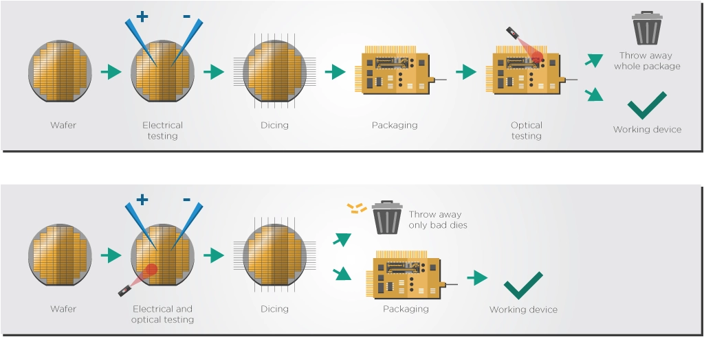
Discrete and partial integration approaches do more of their optical testing on the finalized package, after connecting all the different components together. Should just one of the components not pass the testing process, the complete packaged transceiver would need to be discarded, potentially leading to a massive waste of materials as nothing can be ”fixed” or reused at this stage of the manufacturing process.
Full integration enables earlier optical testing on the semiconductor wafer and dies. By testing the dies and wafers directly before packaging, manufacturers need only discard the bad dies rather than the whole package, which saves valuable energy and materials.
Full Integration Drives Sustainability
While communication networks have become more energy-efficient, further technological improvements must continue decreasing the cost of energy per bit and keeping up with the exponential increase in Internet traffic. At the same time, a greater focus is being placed on the importance of sustainability and responsible manufacturing. All the photonic integration approaches we have touched on will play a role in reducing the energy consumption of future networks. However, out of all of them, only full integration is in a position to make a significant contribution to the goals of sustainability and environmentally friendly manufacturing. A fully integrated system-on-chip minimizes optical losses, transceiver energy consumption, power usage, and materials wastage while at the same time ensuring increased energy efficiency of the manufacturing, packaging, and testing process.