What do Next-Gen Optical Subassemblies Need?
While packaging, assembly, and testing are only a small part of the cost of electronic systems, the reverse happens with photonic integrated circuits (PICs) and their subassemblies. Researchers at the Technical University of Eindhoven (TU/e) estimate that for most Indium Phosphide (InP) photonics devices, the cost of packaging, assembly, and testing can reach around 80% of the total module cost.
To trigger a revolution in the use of photonics worldwide, it needs to be as easy to manufacture and use as electronics. In the words of EFFECT Photonics’ Chief Technology Officer, Tim Koene: “We need to buy photonics from a catalog as we do with electronics, have datasheets that work consistently, be able to solder it to a board and integrate it easily with the rest of the product design flow.”
This article will explore three key avenues to improve optical subassemblies and packaging for photonic devices.
Learning from Electronics Packaging
A key way to improve photonics manufacturing is to learn from electronics packaging, assembly, and testing methods that are already well-known and standardized. After all, building a new special production line is much more expensive than modifying an existing production flow.
One electronic technique essential to transfer into photonics is ball-grid array (BGA) packaging. BGA-style packaging has grown popular among electronics manufacturers over the last few decades. It places the chip connections under the chip package, allowing more efficient use of space in circuit boards, a smaller package size, and better soldering.
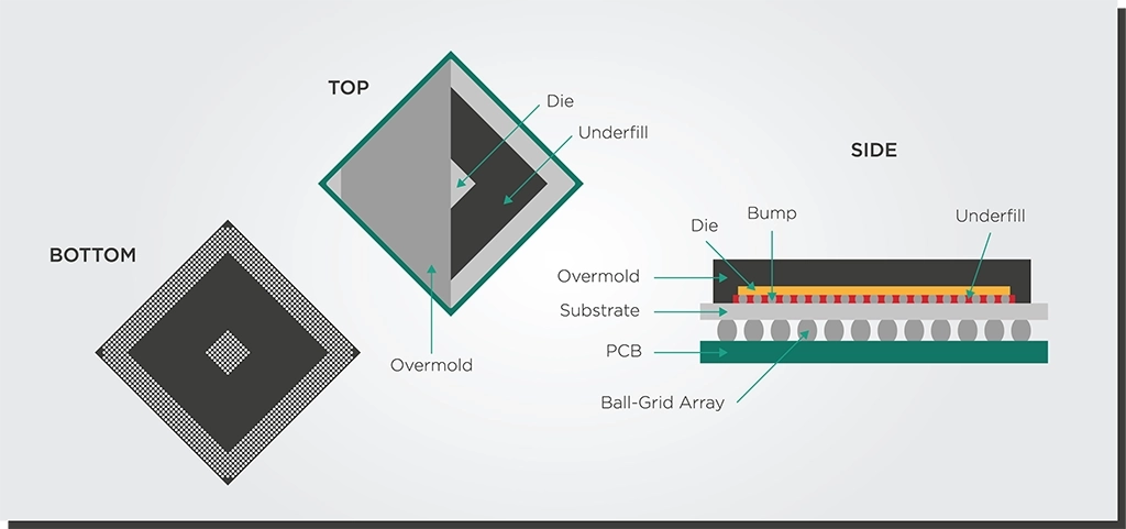
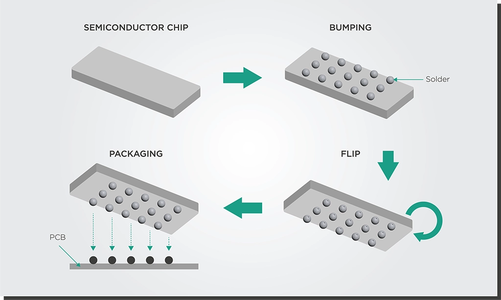
Another critical technique to move into photonics is flip-chip bonding. This process is where solder bumps are deposited on the chip in the final fabrication step. The chip is flipped over and aligned with a circuit board for easier soldering.
These might be novel technologies for photonics developers who have started implementing them in the last five or ten years. However, the electronics industry embraced these technologies 20 or 30 years ago. Making these techniques more widespread will make a massive difference in photonics’ ability to scale up and become as available as electronics.
Adopting BGA-style packaging and flip-chip bonding techniques will make it easier for PICs to survive this soldering process. There is ongoing research and development worldwide, including at EFFECT Photonics, to transfer more electronics packaging methods into photonics. PICs that can handle being soldered to circuit boards allow the industry to build optical subassemblies that are more accessible to the open market and can go into trains, cars, or airplanes.
The Benefits of Increasing Integration
Economics of scale is a crucial principle behind electronics manufacturing, and we must apply it to photonics too. The more components we can integrate into a single chip and the more chips we can integrate into a single wafer, the more affordable the photonic device becomes. If production volumes increase from a few thousand chips per year to a few million, the price per optical chip can decrease from thousands of Euros to mere tens of Euros. This must be the goal for the photonics industry in general.
By integrating all optical components on a single chip, we also shift the complexity from the assembly process to the much more efficient and scalable semiconductor wafer process. Assembling and packaging a device by interconnecting multiple photonic chips increases assembly complexity and costs. On the other hand, combining and aligning optical components on a wafer at a high volume is much easier, which drives down the device’s cost.
Deepening photonics integration will also have a significant impact on power consumption. Integrating all the optical components (lasers, detectors, modulators, etc.) on a single chip can minimize the losses and make devices such as optical transceivers more efficient. This approach doesn’t just optimize the efficiency of the devices themselves but also of the resource-hungry chip manufacturing process.
The Importance of Laser Packaging
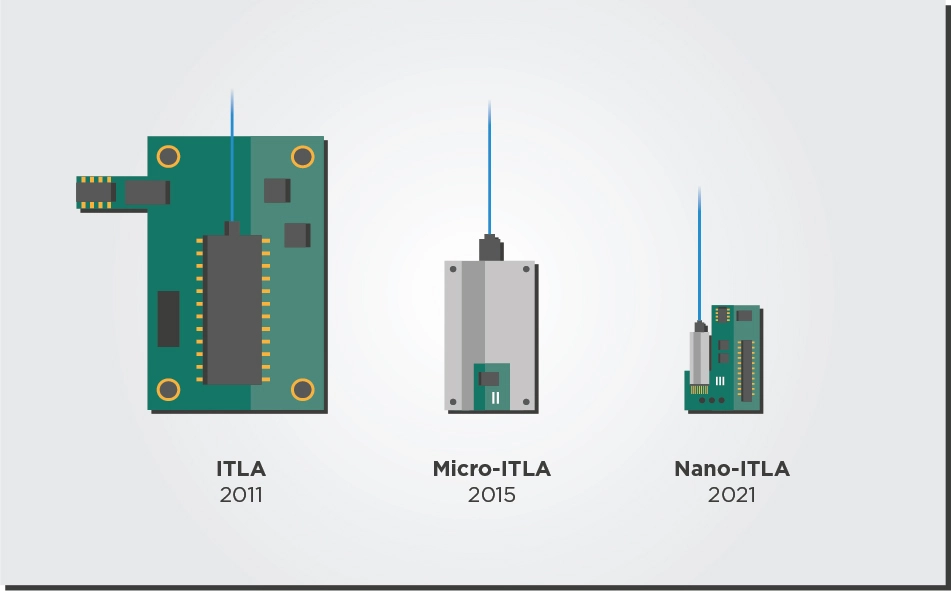
Over the last decade, technological progress in tunable laser packaging and integration has matched the need for smaller footprints. In 2011, tunable lasers followed the multi-source agreement (MSA) for integrable tunable laser assemblies (ITLAs). By 2015, tunable lasers were sold in the more compact Micro-ITLA form factor, which cut the original ITLA package size in half. And in 2019, laser developers (see examples here and here) announced a new Nano-ITLA form factor that reduced the size by almost half again.
Reducing the footprint of tunable lasers in the future will need even greater integration of their parts. For example, every tunable laser needs a wavelength locker component that can stabilize the laser’s output regardless of environmental conditions such as temperature. Integrating the wavelength locker component on the laser chip instead of attaching it externally would help reduce the laser package’s footprint and power consumption.
Another aspect of optimizing laser module footprint is allowing transceiver developers to mix and match their building blocks. For example, traditional ITLAs in transceivers contain the temperature control driver and power converter functions. However, the main transceiver board can usually provide these functions too. A setup in which the main board performs these driver and converter functions would avoid the need for redundant elements in both the main board and tunable laser.
Finally, the future of laser packaging will also involve packaging more multi-laser arrays. As explained in a previous article, multi-laser arrays will become increasingly necessary to increase link capacity in coherent systems. They will not need more slots in the router faceplate while avoiding the higher cost and complexity of increasing the speed with a single laser channel.
Takeaways
Improving subassemblies and packaging is vital for photonics to reach its potential. Photonics must learn from well-established, standardized electronics packaging techniques like BGA-style packaging and flip-chip bonding. By increasing integration, photonics can achieve economies of scale that make devices more affordable and energy efficient. In this context, improved integration and packaging of tunable lasers and arrays will be particularly important. Overall, these efforts will make photonics more accessible to the open market and make it as easy to manufacture and use as electronics.