The Fabrication Process Inside a Photonic Foundry
Photonics is one of the enabling technologies of the future. Light is the fastest information carrier in the universe and can transmit this information while dissipating less heat and energy than electrical signals. Thus, photonics can dramatically increase the speed, reach, and flexibility of communication networks and cope with the ever-growing demand for more data. And it will do so at a lower energy cost, decreasing the Internet’s carbon footprint. Meanwhile, fast and efficient photonic signals have massive potential for sensing and imaging applications in medical devices, automotive LIDAR, agricultural and food diagnostics, and more.
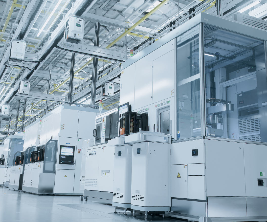
Given its importance, we should discuss the fabrication processes inside photonic semiconductor foundries.
Manufacturing semiconductor chips for photonics and electronics is one of the most complex procedures in the world. For example, back in his university days, EFFECT Photonics co-founder Boudewijn Docter described a fabrication process with 243 steps!
Yuqing Jiao, Associate Professor at the Eindhoven University of Technology (TU/e), explains the fabrication process in a few basic, simplified steps:
- Grow or deposit your chip material
- Print a pattern on the material
- Etch the printed pattern into your material
- Do some cleaning and extra surface preparation
- Go back to step 1 and repeat as needed
Real life is, of course, a lot more complicated and will require cycling through these steps tens of times, leading to processes with more than 200 total steps. Let’s go through these basic steps in a bit more detail.

1. Layer Epitaxy and Deposition: Different chip elements require different semiconductor material layers. These layers can be grown on the semiconductor wafer via a process called epitaxy or deposited via other methods, such as physical or chemical vapor deposition.

2. Lithography (i.e., printing): There are a few lithography methods, but the one used for high-volume chip fabrication is projection optical lithography. The semiconductor wafer is coated with aphotosensitive polymer film called a photoresist. Meanwhile, the design layout pattern is transferred to an opaque material called a mask. The optical lithography system projects the mask pattern onto the photoresist. The exposed photoresist is then developed (like photographic film) to complete the pattern printing.

3. Etching: Having “printed” the pattern on the photoresist, it is time to remove (or etch) parts of the semiconductor material to transfer the pattern from the resist into the wafer. Etching techniques can be broadly classified into two categories.
- Dry Etching: These processes remove material by bombarding it with ions. Typically, these ions come from a plasma of reactive gases like oxygen, boron, chlorine, etc. This approach is often used to etch a material anisotropically (i.e., in a specific direction).
- Wet Etching: These processes involve the removal of material using a liquid reactant. The material to be etched is immersed in the solution, which will dissolve the targeted material layers. This solution usually consists of an acid, such as hydrofluoric acid (HFl), to etch silicon. Wet etching is typically used for etching a material isotropically (i.e., in all directions).

4. Cleaning and Surface Preparation: After etching, a series of steps will clean and prepare the surface before the next cycle.
- Passivation: Adding layers of dielectric material (such as silica) to “passivate” the chip and make it more tolerant to environmental effects.
- Planarization: Making the surface flat in preparation for future lithography and etching steps.
- Metallization: Depositing metal components and films on the wafer. This might be done for future lithography and etching steps or, in the end, to add electrical contacts to the chip.
Figure 5 summarizes how an InP photonic device looks after the steps of layer epitaxy, etching, dielectric deposition and planarization, and metallization.

After this fabrication process ends, the processed wafers are shipped worldwide to be tested and packaged into photonic devices. This is an expensive process we discussed in one of our previous articles.
Takeaways
The process of making photonic integrated circuits is incredibly long and complex, and the steps we described in this article are a mere simplification of the entire process. It requires tremendous knowledge in chip design, fabrication, and testing from experts in different fields worldwide. EFFECT Photonics was founded by people who fabricated these chips themselves, understood the process intimately and developed the connections and network to develop cutting-edge PICs at scale.