EFFECT Photonics: A novel packaging competence that delivers
It is difficult to remember a time before the Internet and wireless communications. Accommodating the tremendous growth in data traffic has been and will continue to be dependent on an ever-expanding fibre optic network. Data centres are increasing in number and size to accommodate the ever-increasing needs for higher data transmission speeds and capacity. At the same time, so-called deep fibre architectures are pushing fibre optics closer to the end users’ homes and buildings. The world is beginning to take advantage of 5G interconnectivity and real-time communication for applications from enhanced mobile broadband and the IoT to mission-critical scenarios of self-driving cars or remotely controlled medical procedures. Low-latency, high-bandwidth optical networks will form the foundations of these technologies.
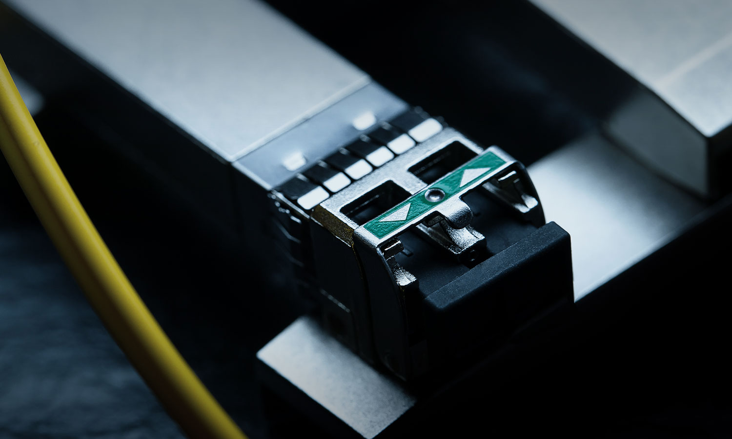
Light as a signal carrier enables much higher data transmission rates over greater distances and with lower losses compared to electrical signals. To encode data into light for transmission and decode it back into electrical signals upon receipt, optical communications rely on optical transceivers. Dense Wavelength Division Multiplexing (DWDM) is transceiver technology that has proved itself indispensable when it comes to adding capacity to existing networks. A standard transceiver, often called a grey transceiver, is a single-channel device – each fibre has a single laser source. DWDM accommodates large numbers of signals carried as different wavelengths of light in a single fibre to route data on different ‘channels’, significantly enhancing bandwidth. Importantly, it is also more flexible and cost-effective to build, own and operate than multiple single-channel point-to-point links.
Full monolithic integration of all photonic components within a single chip (a photonics integrated circuit or PIC) is a key enabler of DWDM technology that achieves these goals. It is by no means industry-standard, but EFFECT Photonics makes it possible. Award-winning System-on-Chip integration of functionalities including the laser, amplification and wavelength locking enables high-density electrical interconnect, minimal optical loss, and simplified production and testing relative to systems built in manual processes from individual components. The result is enhanced optical transmission with low energy consumption, reduced cost, and significantly smaller physical size of the module.
The PIC technology creates even more benefits by facilitating cost-effective packaging solutions. EFFECT Photonics proprietary packaging technology is developed and implemented in-house. This not only gives us the ability to tailor packaging to our PICs but also reduces the time and cost associated with development and testing. Importantly, it provides greater independence from market fluctuations and global uncertainties and generates supply security.
Dr. Paul Rosser, Chief Operations Officer at EFFECT Photonics, summarises: “Optical communication is used for increasingly shorter distances thanks to growing system performance and bandwidth requirements. As a result, innovative packaging approaches are needed that closely integrate optical technology within the system. Nowadays, pluggable transceivers are implemented at the system edge. In addition, embedded optical modules for onboard assembly are becoming more apparent in bandwidth-intensive applications. The first high-performance computing systems where optical transceivers are mounted onto the switch chip package have already entered the market. However, more widespread adoption of optical link technology is limited by cost and assembly activities involving optics. EFFECT Photonics applies integration strategies across all levels to improve optics’ performance and functionality, while lowering cost.”
The robotics foundations required for volume packaging are in place. As EFFECT Photonics rapidly expands its product portfolio with a diverse range of technologies, either additional standardised and modular packaging solutions or many customised ones are required. The company is pursuing funding and investment opportunities to enhance packaging capabilities in two critical ways. The first is expanding both the number and specialisation of talented and motivated scientists and engineers in various fields, including mechatronics and software development and testing. Photonics is a relatively new and quite diverse field. The ability to train qualified new hires in specialised areas such as packaging, automation, and data analysis relevant to EFFECT Photonics will significantly augment current capabilities. Second, producing in volume with high yield at low cost will also require associated infrastructure expansion.
EFFECT Photonics is uniquely positioned to become a global supplier of choice for optical transceivers thanks to its cost-effective and high-performance optical System-on-Chip design, innovative electronics for high-speed capability and unique non-hermetic packaging technology supporting scaling in volume cost-effectively. This novel packaging competence allows our company to offer customers significant savings without compromising the performance they expect.
For more information, please contact us at info@effectphotonics.com