How To Make a Photonic Integrated Circuit
Photonics is one of the enabling technologies of the future. Light is the fastest information carrier in the universe and can transmit this information while dissipating less heat and energy than electrical signals. Thus, photonics can dramatically increase the speed, reach, and flexibility of communication networks and cope with the ever-growing demand for more data. And it will do so at a lower energy cost, decreasing the Internet’s carbon footprint. Meanwhile, fast and efficient photonic signals have massive potential for sensing and imaging applications in medical devices, automotive LIDAR, agricultural and food diagnostics, and more.
Given its importance, we want to explain how photonic integrated circuits (PICs), the devices that enable all these applications, are made.
Designing a PIC
The process of designing a PIC should translate an initial application concept into a functioning photonics chip that can be manufactured. In a short course at the OFC 2018 conference, Wim Bogaerts from Ghent University summarized the typical PIC design process in the steps we will describe below.

- Concept and Specifications: We first have to define what goes into the chip. A chip architect normally spends time with the customer to understand what the customer wants to achieve with the chip and all the conditions and situations where the chip will be used. After these conversations, the chip application concept becomes a concrete set of specifications that are passed on to the team that will design the internals of the chip. These specs will set the performance targets of the PIC design.
- Design Function: Having defined the specs, the design team will develop a schematic circuit diagram that captures the function of the PIC. This diagram is separated into several functional blocks: some of them might already exist, and some of them might have to be built. These blocks include lasers, modulators, detectors, and other components that can manipulate light in one way or another.
- Design Simulation: Making a chip costs a lot of money and time. With such risks, a fundamental element of chip design is to accurately predict the chip’s behavior after it is manufactured. The functional blocks are placed together, and their behavior is simulated using various physical models and simulation tools. The design team often uses a few different simulation approaches to reduce the risk of failure after manufacturing.
- Design Layout: Now, the design team must translate the functional chip schematic into a proper design layout that can be manufactured. The layout consists of layers, component positions, and geometric shapes that represent the actual manufacturing steps. The team uses software that translates these functions into the geometric patterns to be manufactured, with human input required for the trickiest placement and geometry decisions.
- Check Design Rules: Every chip fabrication facility will have its own set of manufacturing rules. In this step, the design team verifies that the layout agrees with these rules.
- Verify Design Function: This is a final check to ensure that the layout actually performs as was originally intended in the original circuit schematic. The layout process usually leads to new component placement and parasitic effects that were not considered in the original circuit schematic. These tests might require the design team to revisit previous functional or layout schematic steps.
The Many Steps of Fabricating a PIC
Manufacturing semiconductor chips for photonics and electronics is one of the most complex procedures in the world. For example, back in his university days, EFFECT Photonics President Boudewijn Docter described a fabrication process with a total of 243 steps!
Yuqing Jiao, Associate Professor at the Eindhoven University of Technology (TU/e), explains the fabrication process in a few basic, simplified steps:
- Grow or deposit your chip material
- Print a pattern on the material
- Etch the printed pattern into your material
- Do some cleaning and extra surface preparation
- Go back to step 1 and repeat as needed
Real life is, of course, a lot more complicated and will require cycling through these steps tens of times, leading to processes with more than 200 total steps. Let’s go through these basic steps in a bit more detail.

- Layer Epitaxy and Deposition: Different chip elements require different semiconductor material layers. These layers can be grown on the semiconductor wafer via a process called epitaxy or deposited via other methods (which are summarized in this article).

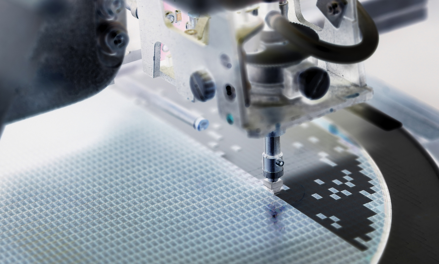
- Lithography (i.e. printing): There are a few lithography methods, but the one used for high-volume chip fabrication is projection optical lithography. The semiconductor wafer is coated with a photosensitive polymer film called a photoresist. Meanwhile, the design layout pattern is transferred to an opaque material called a mask. The optical lithography system projects the mask pattern onto the photoresist. The exposed photoresist is then developed (like photographic film) to complete the pattern printing.

- Etching: Having “printed” the pattern on the photoresist, it is time to remove (or etch) parts of the semiconductor material to transfer the pattern from the resist into the wafer. There are several techniques that can be done to etch the material, which are summarized in this article.

- Cleaning and Surface Preparation: After etching, a series of steps will clean and prepare the surface before the next cycle.
- Passivation: Adding layers of dielectric material (such a silica) to “passivate” the chip and make it more tolerant to environmental effects.
- Planarization: Making the surface flat in preparation of future lithography and etching steps.
- Metallization: Depositing metal components and films on the wafer. This might be done for future lithography and etching steps, or at the end to add electrical contacts to the chip.
Figure 6 summarizes how an InP photonic device looks after the steps of layer epitaxy, etching, dielectric deposition and planarization, and metallization.

The Expensive Process of Testing and Packaging
Chip fabrication is a process with many sources of variability, and therefore much testing is required to make sure that the fabricated chip agrees with what was originally designed and simulated. Once that is certified and qualified, the process of packaging and assembling a device with the PIC follows.
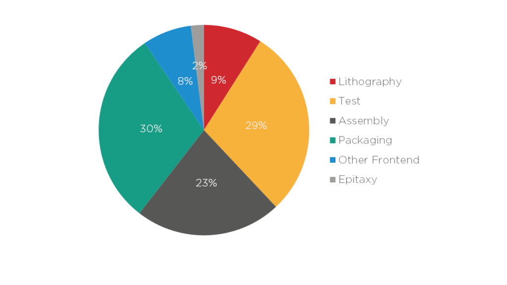
While packaging, assembly, and testing are only a small part of the cost of electronic systems, the reverse happens with photonic systems. Researchers at the Technical University of Eindhoven (TU/e) estimate that for most Indium Phosphide (InP) photonics devices, the cost of packaging, assembly, and testing can reach around 80% of the total module cost. There are many research efforts in motion to reduce these costs, which you can learn more about in one of our previous articles.
Especially after the first fabrication run of a new chip, there will be a few rounds of characterization, validation and revisions to make sure the chip performs up to spec. After this first round of characterization and validation, the chip must be made ready for mass production, which requires a series of reliability tests in several environmental different conditions. You can learn more about this process in our previous article on industrial hardening. For example, different applications need different certification of the temperatures in which the chip must operate in.
| Temperature Standard | Temperature Range (°C) | |
| Min | Max | |
| Commercial (C-temp) | 0 | 70 |
| Extended (E-temp) | -20 | 85 |
| Industrial (I-temp) | -40 | 85 |
| Automotive / Full Military | -40 | 125 |
Takeaways
The process of making photonic integrated circuits is incredibly long and complex, and the steps we described in this article are a mere simplification of the entire process. It requires tremendous amount of knowledge in chip design, fabrication, and testing from experts in different fields all around the world. EFFECT Photonics was founded by people who fabricated these chips themselves, understand the process intimately, and developed the connections and network to develop cutting-edge PICs at scale.