Japan Innovation Mission
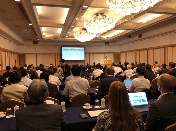
Last week, Tim Koene (CTO) and Sophie De Maesschalck (CFO) of EFFECT Photonics, traveled to Japan on a semiconductor innovation mission with several other top Dutch businesses. The mission was jointly organized by the Netherlands Enterprise Agency (RVO), the Innovation Attaché Tokyo and the Dutch Embassy.
As the world’s third-largest economy, Japan has a long and established history in the semiconductor field. The purpose of the mission was to offer an opportunity for exploring and finding potential partners for joint research, development, and commercialization of innovation in this space, with a strong focus on integrated photonics. In addition, the aim was to further build on the strong relationship and develop bilateral agreements and programs between the two governments.
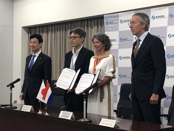
During the innovation mission, the two countries signed a Memorandum of Cooperation on semiconductor policies where both governments will work to facilitate both private and public sector collaboration on semiconductor and related technologies such as photonics.
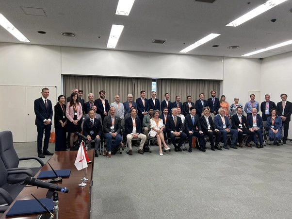
The high-quality interactions, high turnout at every event during the week, and the media coverage shows the importance Japan is placing on the partnership with the Netherlands in the field of Semiconductors. The personal involvement of Minister Nishimura doubly underlines this. It is clear that Integrated Photonics is a key pillar in the broader Semiconductor policy. The support of the Ministry of Economic Affairs and Climate to organize this Innovation Mission is greatly appreciated. We have done more in one week than we could have done in a dozen visits.
Tim Koene, CTO at EFFECT Photonics