Wafer Scale Photonics for a Coherent Future
The advances in electronic and optical integration have brought down the size and cost of the coherent transceivers, packing more bits than ever into smaller areas. However, progress in the cost and bandwidth density of transceivers might slow down soon. Electronics has achieved amazing breakthroughs in the last two decades to continue increasing transistor densities and keeping Moore’s Law alive, but these achievements have come at a price. With each new generation of electronic processors, development costs increase and the price per transistor has stagnated.
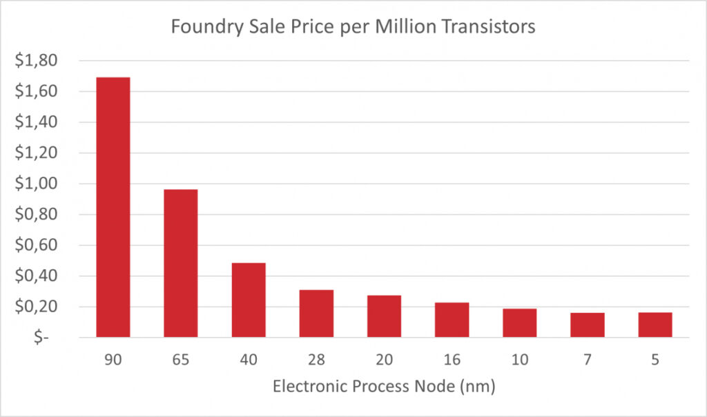
Due to these developments, electronic digital signal processor (DSP) chips will continue to improve in efficiency and footprint, but their price will stagnate and with it the price of optical transceivers. Without further improvements in the cost per bit, it will be difficult to achieve the goal of making coherent technology more accessible across the entire optical network. This will make it more difficult to provide the device volume and services needed by the growing 5G networks and cloud providers.
To make coherent transceivers more accessible, photonics has to step up now more than ever. With the cost of DSPs stagnating, photonic integration must take the lead in driving down the costs and size of optical transceivers. Integrating all optical components on a single chip makes it easier to scale up in volume, reach these size and cost targets, and ultimately provide faster, more affordable, and sustainable coherent transmission.
Size Matters
Full photonic integration allows us to combine active optical elements like the laser and the amplifer with passive elements, all on the same chip and enclosed in a simple, non-hermetic package. This process enables a much smaller device than combining several indivudally packaged elements. For example, by integrating all photonic functions on a single chip, including lasers and optical amplifiers, EFFECT Photonics’ pluggable transceiver modules can achieve transmit power levels similar to those of line card transponder modules while still keeping the smaller QSFP router pluggable form factor, power consumption, and cost.
Full integration technology increases the transmit power by minimizing the optical losses due to the use of more efficient optical modulators, fewer material losses compared to silicon, and the integration of the laser device on the same chip as the rest of the optical components. The semiconductor optical amplifiers (SOAs) used in fully integrated devices can also outperform the performance of micro-EDFAs for transmission distances of at least 80km.
The Economics of Scale
As innovative as full photonic integration can be, it will have little impact if it cannot be manufactured at a high enough volume to satisfy the demands of mobile and cloud providers and drive down the cost per device. Wafer scale photonics manufacturing demands a higher upfront investment, but the resulting high-volume production line drives down the cost per device. This economy-of-scale principle is the same one behind electronics manufacturing, and the same must be applied to photonics.
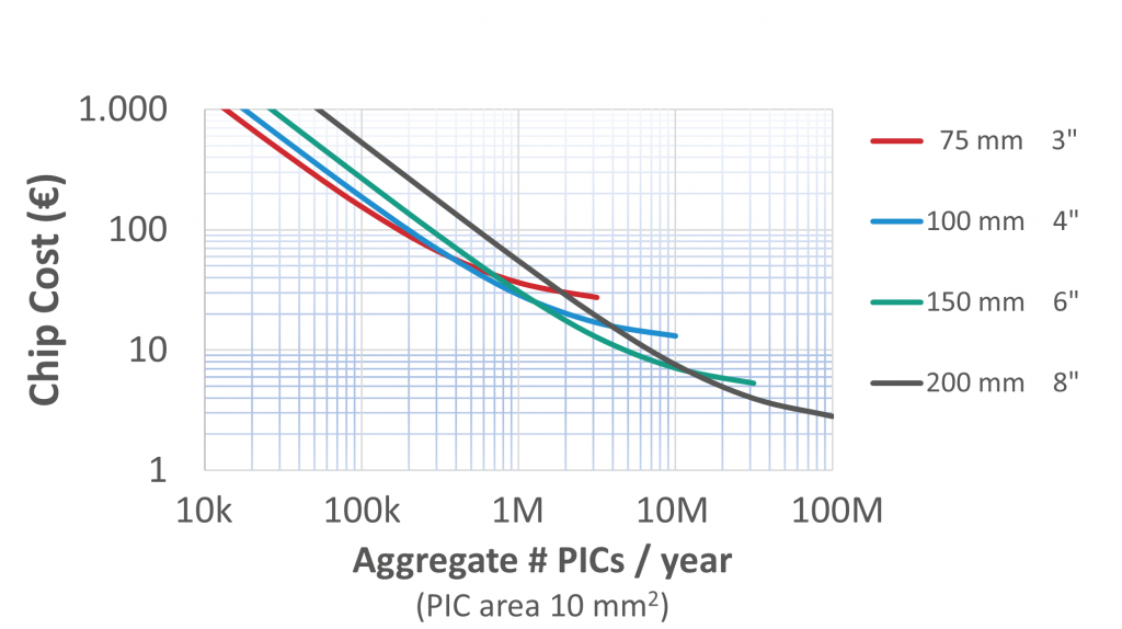
The more optical components we can integrate into a single chip, the more can the price of each component decrease. The more optical System-on-Chip (SoC) devices can go into a single wafer, the more can the price of each SoC decrease. Researchers at the Technical University of Eindhoven and the JePPIX consortium have done some modelling to show how this economy of scale principle would apply to photonics. If production volumes can increase from a few thousands of chips per year to a few millions, the price per optical chip can decrease from thousands of Euros to mere tens of Euros. This must be the goal for the optical transceiver industry.
Full Integration Streamlines Production and Testing
Integrating all optical components on a single chip can make manufacturing and testing more efficient, sustainable, and easier to scale up. The price of photonic devices is not dominated by the manufacturing of the semiconductor chips, but by the device assembly and packaging. Assembling and packaging a device by interconnecting multiple photonic chips together leads to an increase in assembly complexity and therefore additional costs.
This situation happens frequently with the laser component, which is often manufactured on a separate chip and then interconnected to the other optical components which are on another chip. Integrating all components—including the laser—on a single chip shifts the complexity from the assembly process to the much more efficient and scalable semiconductor wafer process. For example, it’s much easier to combine optical components on a wafer at a high-volume than it is to align different chips together in the assembly process, and that drives down the cost of the device.
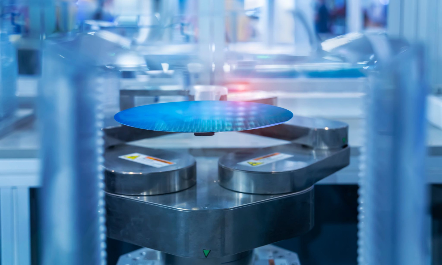
Testing is another aspect that becomes more efficient and scalable when manufacturing at the wafer level. When faults are found earlier in the testing process, fewer resources and energy are spent in process defective chips. Ideally, testing should happen not only on the final, packaged transceiver but in the earlier stages of PIC fabrication, such as measuring after wafer processing or cutting the wafer into smaller dies.
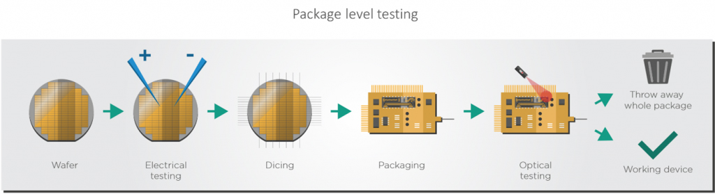
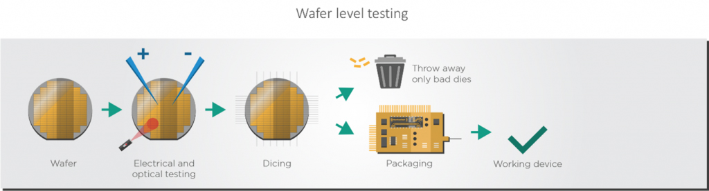
Full photonic integration enables earlier optical testing on the semiconductor wafer and dies. By testing the dies and wafers directly before packaging, manufacturers need only discard the bad dies rather than the whole package, which saves time, cost, and is more energy efficient and sustainable. For example, EFFECT Photonics reaps these benefits in its production processes. 100% of electrical testing on the PICs happens at the wafer level, and our unique integration technology allows for 90% of optical testing to also happen on the wafer.
Takeaways
Photonics is facing the next stage of its development. There have been many great breakthroughs that have allowed us to take photonic devices from the lab to real-world use cases. However, to have the biggest possible impact in society, we need to manufacture photonic devices at very high volumes to make them accessible to everyone. This requires us to think about production volumes in the scale of millions of units. At EFFECT Photonics, we believe that the way to achieve this goal is by following the blueprint laid out by our friends in the electronics industry. By integrating all optical components on a single chip, we can shift more complexity from the assembly to the wafer, allowing production to scale more efficiently and sustainably. In our next article, we will elaborate on another key factor of the electronics blueprint: the fabless development model.