Leveraging the Power of External Foundries in Photonics
Working with a world-class high-volume foundry makes scaling up from low to high volume as easy as putting a purchase order in place. Instead of having to buy equipment, develop processes, and train operators over many years, a fabless photonics developer can leverage foundries who already have these capabilities and knowledge.
Thanks to wafer scale technology, electronics has successfully driven down cost per transistor for many decades. This allowed the world to enjoy chips that every generation became smaller and provided exponentially more computing power for the same amount of money. This scale-up process is how everyone now has a computer processor in their pocket that is millions of times more powerful than the most advanced computers of the 1960s that landed men on the moon.
This progress in electronics integration is a key factor that brought down the size and cost of coherent transceivers, packing more bits than ever into smaller areas. However, photonics has struggled to keep up with electronics, and now the optics dominate the optical transceiver’s cost. If the transceiver cost curve does not continue to decrease, it will be difficult to achieve the goal of making coherent technology more accessible across the entire optical network. This will make it more difficult to provide the services needed by cloud providers and the growing 5G access networks.
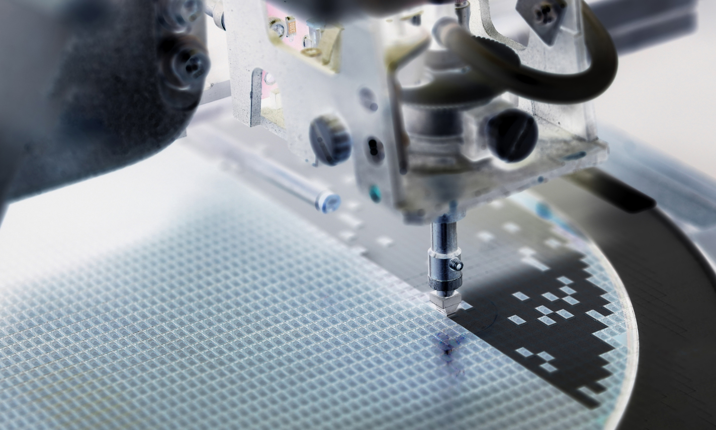
As we mentioned in our previous article, photonics manufacturing must move into wafer-scale territory to provide faster, more affordable, and sustainable coherent transmission.
However, most photonic chip developers don’t have human and financial resources to own and operate their own wafer-scale photonic foundries. Fortunately, electronic chip developers have shown a more viable and cost-effective alternative: the fabless model.
A Lower Upfront Investment
Increasing the volume of photonics manufacturing is a big challenge. Some photonic chip developers choose to manufacture their chips in-house within their own fabrication facilities. This approach has some strong advantages, as it gives component manufacturers full control over their production process. By vertically integrating the whole chip design, manufacturing, and testing process within the same company, it’s often easier to try out new changes and innovations to the product.
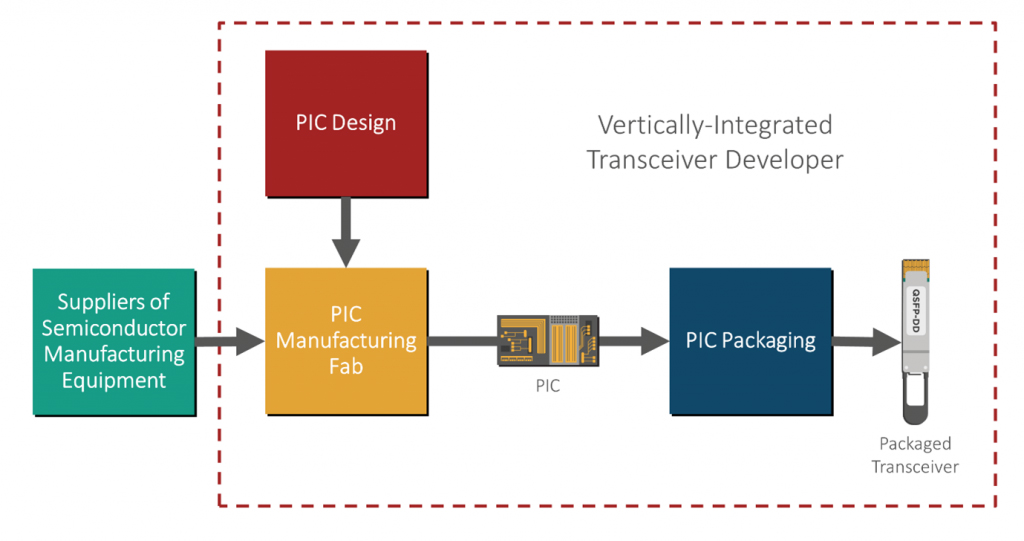
However, this approach has its trade-offs. If a vertically-integrated chip developer wants to scale up in volume, they must make a hefty investment in more equipment and personnel to do so. They must develop new fabrication process which not only need money, but also time to develop and train personnel. Especially in the case of an optical transceiver market that is not as big as that of consumer electronics, it’s hard not to wonder whether that initial investment is cost-effective.
Electronics manufacturing had a similar problem during their 1970s boom, with smaller chip start-ups facing almost insurmountable barriers to enter the market because of the massive capital expenditure (CapEx) required. Electronics solved this problem by moving into what we call a fabless model, with companies designing and selling the chips but outsourcing the manufacturing.
For example, transceiver DSP chip developers design the chip, but then outsource the actual fabrication to a large-volume manufacturing plant (usually called a foundry). This business model works by leveraging the design, research, development, and distribution networks of the fabless company, and the specialized manufacturing skill of the chip foundry.
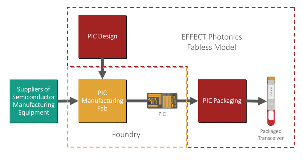
This model reduces the capital expenditure burden on the DSP developers, because instead of spending all the time and energy in scaling up their own facilities, they can work with a foundry that already did that investment and has the required manufacturing volume. In other words, instead going through a more costly, time-consuming process, the troubles of scaling up are outsourced and (from the perspective of the fabless company) become as simple as putting a purchase order in place. Furthermore, the fabless model also allows companies to concentrate their R&D resources on the end market. If photonics is to move into million-scale volumes, this is likely the way forward.
Economies of Scale and Operating Expenses
Even if an optical transceiver developer could move forward with the CapEx required for its own large-scale fab and a vertically-integrated model, market demand and operational expenses become the next pain point. Transceivers are a B2B market, and their demand is significantly smaller than of B2C consumer electronics. For example, LightCounting estimates that 55 million optical transceivers will be sold in 2021, while the International Data Corporation estimates that 1.4 billion smartphones will be sold in 2021. The latter figure is 25 times larger than that of the transceiver market.
The smaller demand of transceivers means that even if a vertically-integrated transceiver developer upgrades to a larger-scale manufacturing facility, it will likely have more manufacturing capacity than what their customers need. In such a situation, the facility could run at a reduced capacity. However, fabs are not only expensive to build, but also to operate. Unless they can be kept at nearly full utilization, operating expenses (OpEx) will become a drain on the finances of the facility owners.
This issue was something the electronics industry faced in the past, during the 1980s. Integrated electronics manufacturers had excess production capacity, and this situation paved the way for the fabless model too. The large-scale manufacturers ended up selling that excess capacity to smaller, fabless chip developers. Ultimately, the entire electronics industry relied increasingly on the fabless model, to the point where pure play foundries like the Taiwan Semiconductor Manufacturing Corporation (TSMC) appeared and focused entirely on manufacturing for other fabless companies.
In this scenario, everyone ended up winning. The foundries serviced multiple companies and could run their facilities at full capacity, while the fabless companies could outsource manufacturing and reduce their expenditures.
Working with the Best in the Business
The other advantage of pure play foundries is that they not only have state-of-the art equipment but also the best personnel and technical expertise. Even if a vertically-integrated developer transceiver can make the required CapEx to scale up their facilities, developing processes and training people inevitably takes years, delaying the return on investment even further.
By working with an established and experienced foundry, fabless companies take advantage of the highly trained and experience personnel of these facilities. These operators, technicians, and engineers have worked day in, day out with their equipment for years and already developed processes that are finely tuned to their equipment. Thanks to their work, fabless transceiver developers do not have to reinvent the wheel and come up with their own processes, saving valuable time and many, many headaches.
Takeaways
To make transceivers more accessible to world and connect more people together, transceiver developers need to reach production scales in the millions. At EFFECT Photonics, we believe that the way to achieve this goal is by having photonics follow the blueprint laid out by the electronics industry. Using a fabless model, we can reduce the capital expenditure and scale up more quickly and with fewer risks.
Working with a world-class high-volume foundry makes scaling up from low to high volume as easy as putting a purchase order in place. Instead of having to buy equipment, develop processes, and train operators over many years, a fabless photonics developer can leverage foundries who already have these capabilities and knowledge.