
Manufacturing a Coherent Transceiver
Coherent transmission has become a fundamental component of optical networks to address situations where direct detect technology cannot provide the required capacity and reach.
While direct detect transmission only uses the amplitude of the light signal, coherent optical transmission manipulates three different light properties: amplitude, phase, and polarization. These additional degrees of modulation allow for faster optical signals without compromising on transmission distance. Furthermore, coherent technology enables capacity upgrades without replacing the expensive physical fiber infrastructure in the ground.
Given the importance of coherent transmission, we will explain some key aspects of manufacturing and testing these devices in this article. In the previous article, we described critical aspects of the transceiver design process.
Into the Global Supply Chain
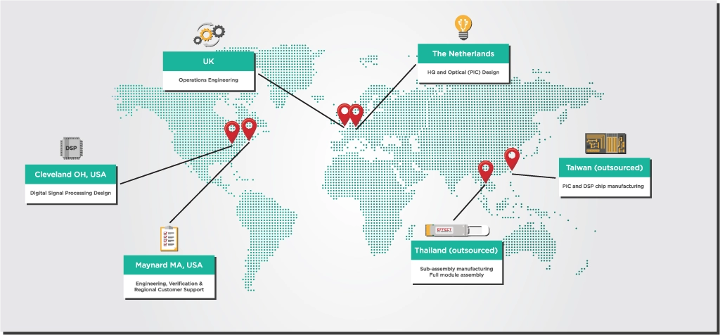
Almost every modern product results from global supply chains, with components and parts manufactured in facilities worldwide. A pluggable coherent transceiver is not an exception. Some transceiver developers will have fabrication facilities in-house, while others (like EFFECT Photonics) are fabless and outsource their manufacturing. We have discussed the pros and cons of these approaches in a previous article.
Writing a faithful, nuanced summary of all the manufacturing processes involved is beyond the scope of this article. Still, we will mention in very broad terms some of the key processes going on.
- Commercial Off The Shelf (COTS) Procurement: Many components in the transceiver are designed in-house and custom-ordered and manufactured, but other components are sourced off-the-shelf from various suppliers and manufacturers. This includes devices such as RF drivers, amplifiers, or even optical sub-assemblies.
- Integrated Circuit Fabrication: The electronic digital signal processor, optical engine, and laser chips are manufactured through semiconductor foundry processes. In the case of EFFECT Photonics, the laser and optical engine can be fabricated on the same chip. You can read some of our previous to know more about what goes into the DSP and the PIC manufacturing processes.
- Manufacturing Sub-Assemblies: When the chips have been manufactured and tested, the manufacturing of the different transceiver sub-assemblies (chiefly the transmitter and receiver) can proceed. Again, vertically-integrated transceiver developers can manufacture these in-house, but most transceiver makers outsource this, especially if they want large-scale production. This includes manufacturing printed circuit boards (PCB) that integrate and interconnect the electronic and optical components. Careful alignment and bonding of optical components, such as lasers and photodetectors, are critical to achieve optimum performance.
- Transceiver Housing: The transceiver subassemblies will be housed in a metal casing, usually made from an aluminum alloy. The design and manufacturing of these housings must consider power distribution and thermal management.
The collaboration in this global supply chain ensures the availability of specialized expertise and resources, leading to efficient and cost-effective production.
Testing the Transceiver
The avid reader may have noticed that we did not mention one of the most critical aspects of manufacturing in the previous section: testing. After all, what you do not test, you cannot manufacture reliably.
Testing and quality assurance processes must occur throughout all the manufacturing processes to verify its performance and compliance with industry standards. Semiconductor chips and PCBs must be tested before they are placed in sub-assemblies. The completed sub-assemblies must then be tested for optical and electrical performance. Once the transceiver module is completed, it must undergo several reliability and compatibility tests. Let’s discuss some of these testing processes.
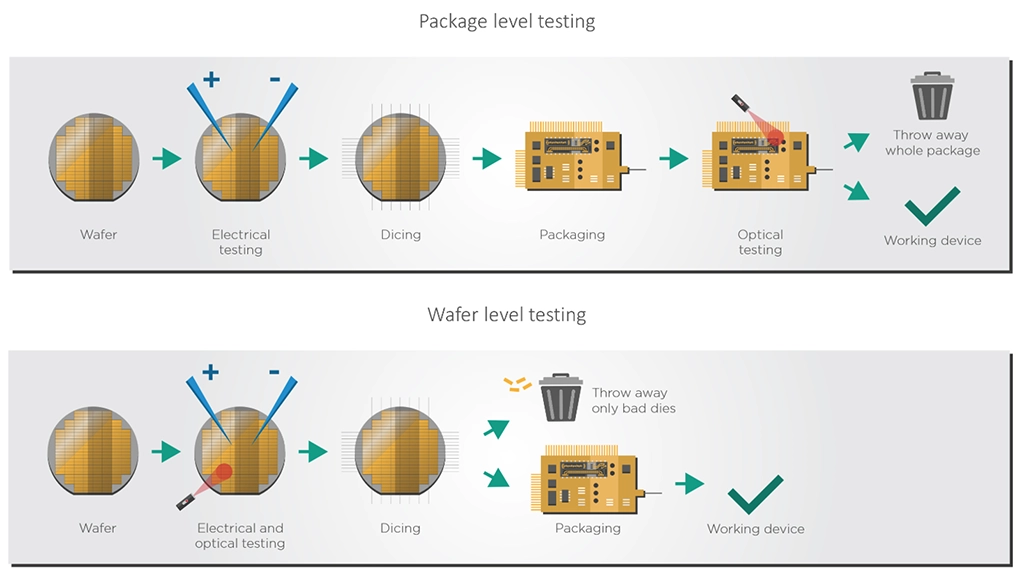
- Chip Testing: Testing should happen not only on the transceiver sub-assemblies or the final package but also after chip fabrication, such as measuring after wafer processing or cutting the wafer into smaller dies. The earlier faults can be found in the testing process, the greater the impact on the use of materials and the energy used to process defective chips.
- Calibration and Performance Testing: This involves assessing and calibrating the key performance parameters of the transceiver: output power, extinction ratio, bit error rate, receiver sensitivity, peak wavelength and spectrum, and a few others. Various modulation formats and data rates should be tested to ensure reliable performance under different operating conditions, and performance at different temperatures is also measured (more on that later). These tests will determine whether the device complies with industry standards.
- Environmental and Reliability Testing: The transceiver should undergo environmental and reliability testing to assess its performance under different operating conditions. These tests ensure that the transceiver can withstand real-world deployment scenarios and maintain reliable operation over its intended lifespan. As shown in Table 1, this includes temperature cycling, humidity testing, vibration testing, and accelerated aging tests.
| Mechanical Reliability & Temperature Testing | ||
|---|---|---|
| Shock & Vibration | High / Low Storage Temp | Temp Cycle |
| Damp Heat | Cycle Moisture Resistance | Hot Pluggable |
| Mating Durability | Accelerated Aging | Life Expectancy Calculation |
- Compatibility Testing: The modules are inserted into switches of various third-party brands to test their interoperability. This is particularly important for a device that wants to be certified by a specific Multi-Source Agreement (MSA) group. This certification adds credibility and ensures that the transceiver can seamlessly integrate into various network environments.
Takeaways
Manufacturing pluggable coherent transceivers involves a global supply chain, enabling access to specialized expertise and resources for efficient production. Some critical processes in this manufacturing chain include procuring materials and off-the-shelf components, fabricating the integrated circuits, and manufacturing the sub-assemblies and the transceiver housing.
Testing and quality assurance are integral to reliable manufacturing. Rigorous testing occurs at various stages, including chip, calibration, performance, environmental, and compatibility testing with third-party brands. This ensures that the transceivers meet industry standards and perform optimally under various operating conditions.
Through meticulous manufacturing and rigorous testing processes, coherent transceivers remain at the forefront of advancing global connectivity.