Thanks to wafer-scale technology, electronics have driven down the cost per transistor for many decades.…
Thanks to wafer-scale technology, electronics have driven down the cost per transistor for many decades. This allowed the world to enjoy chips that every generation became smaller and provided exponentially more computing power for the same amount of money. This scale-up process is how everyone now has a computer processor in their pocket that is millions of times more powerful than the most advanced computers of the 1960s that landed men on the moon.
For example, this progress in electronics integration is a key factor that brought down the size and cost of coherent transceivers, packing more bits than ever into smaller areas. However, photonics has struggled to keep up with electronics, with the photonic components dominating the cost of transceivers. Making transceivers more accessible across the entire optical network requires bringing down these costs.
In this article, we will explore a bit of the relationship between optics and semiconductors and explain what optics can learn from electronics when it comes to semiconductor processes.
At the Heart of Photonic Systems
Semiconductor materials are vital for photonics due to their electronic and optical properties. These materials have a bandgap that can be precisely manipulated to control the absorption and emission of light, and this is essential for creating photonic devices like lasers and photodetectors. The ability to engineer the electronic structure of semiconductors like silicon, gallium arsenide (GaAs), and indium phosphide (InP) allows for the design of devices that operate across various wavelengths of light. These capabilities allow us to develop efficient, compact, and versatile photonic components.
Moreover, semiconductor fabrication techniques, inherited from the microelectronics industry, enable the mass production of photonic devices, which supports scalability and integration of photonics with existing electronic systems. If photonics becomes as readily available and easy to use as electronics, it can become more widespread and have an even greater impact on the world.
“We need to buy photonics from a catalog as we do with electronics, have datasheets that work consistently, be able to solder it to a board and integrate it easily with the rest of the product design flow.“
Tim Koene – Chief Technology Officer, EFFECT Photonics
Some differences between electronics and photonics complicate this transition. Silicon, the dominant material in microelectronics, cannot naturally emit laser light from electrical signals. Therefore, making suitable components for integrated photonics often requires using III-V semiconductor materials such as InP and GaAs. The need for these non-silicon semiconductors has made the photonics manufacturing space harder to standardize and streamline than microelectronics.
The Need for a Fabless Model
Increasing the volume of photonics manufacturing is a big challenge. Some photonic chip developers manufacture their chips in-house within their fabrication facilities. This approach has some substantial advantages, giving component manufacturers complete control over their production process.
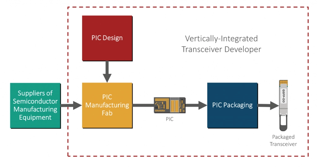
However, this approach has its trade-offs when scaling up. If a vertically-integrated chip developer wants to scale up in volume, they must make a hefty capital expenditure (CAPEX) in more equipment and personnel. They must develop new fabrication processes as well as develop and train personnel. Fabs are not only expensive to build but to operate. Unless they can be kept at nearly full utilization, operating expenses (OPEX) also drain the facility owners’ finances.
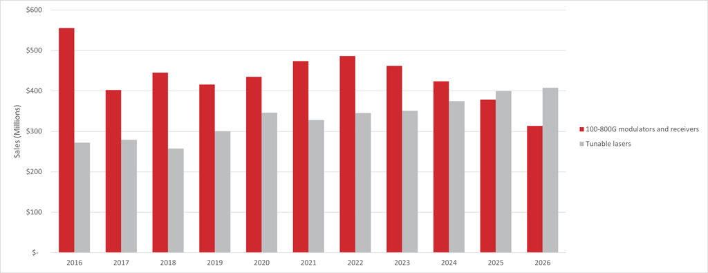
Especially in the case of an optical transceiver market that is not as big as that of consumer electronics, it’s hard not to wonder whether that initial investment is cost-effective. For example, LightCounting estimates that 55 million optical transceivers were sold in 2021, while the International Data Corporation estimates that 1.4 billion smartphones were sold in 2021. The latter figure is 25 times larger than that of the transceiver market.
Electronics manufacturing experienced a similar problem during their 70s and 80s boom, with smaller chip start-ups facing almost insurmountable barriers to market entry because of the massive CAPEX required. Furthermore, the large-scale electronics manufacturing foundries had excess production capacity that drained their OPEX. The large-scale foundries ended up selling that excess capacity to the smaller chip developers, who became fabless. In this scenario, everyone ended up winning. The foundries serviced multiple companies and could run their facilities at total capacity, while the fabless companies could outsource manufacturing and reduce their expenditures.
This fabless model, with companies designing and selling the chips but outsourcing the manufacturing, should also be the way to go for photonics. Instead of going through a more costly, time-consuming process, the troubles of scaling up for photonics developers are outsourced and (from the perspective of the fabless company) become as simple as putting a purchase order in place. Furthermore, the fabless model allows photonics developers to concentrate their R&D resources on the end market. This is the simplest way forward if photonics moves into million-scale volumes.
Investment is Needed for Photonics to Scale like Electronics
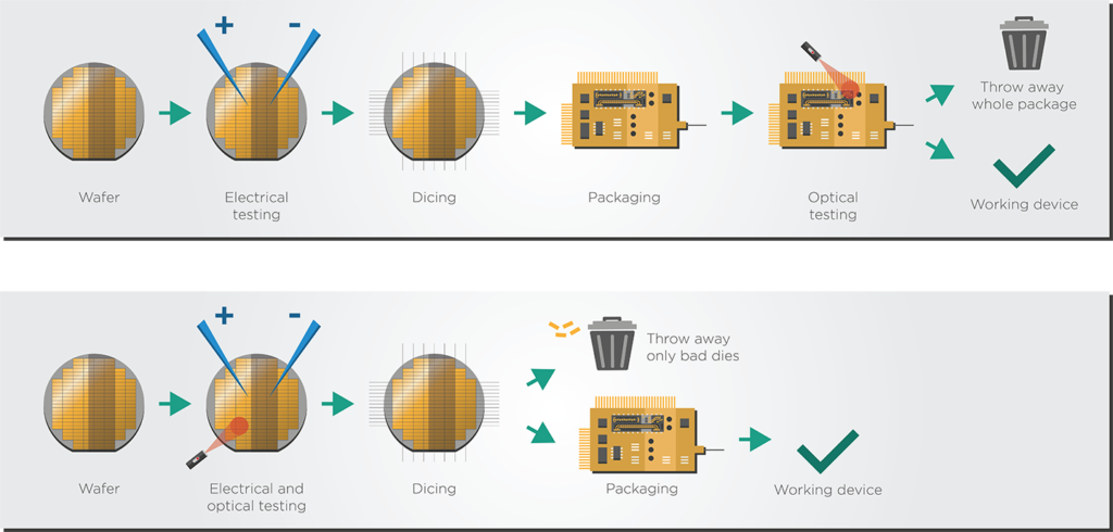
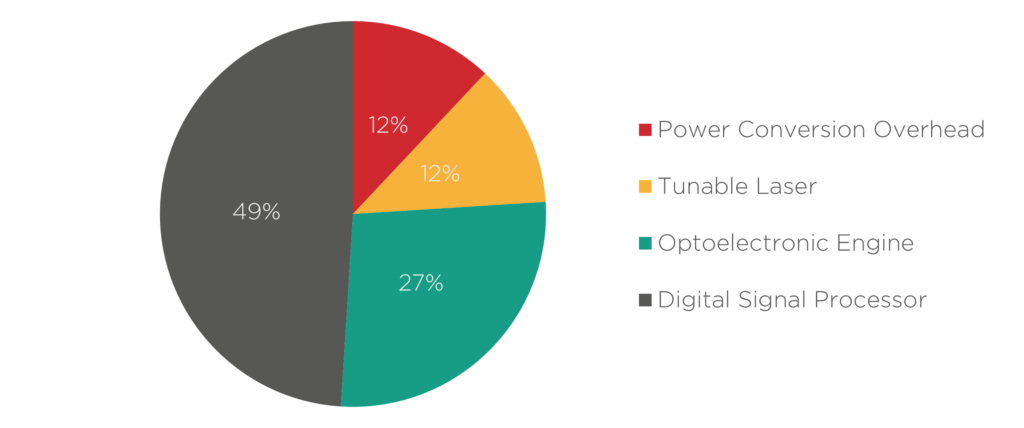
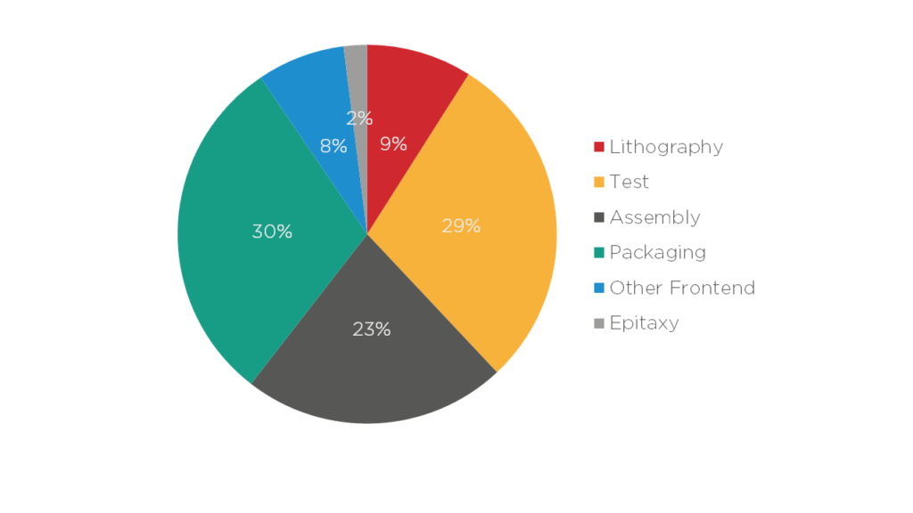
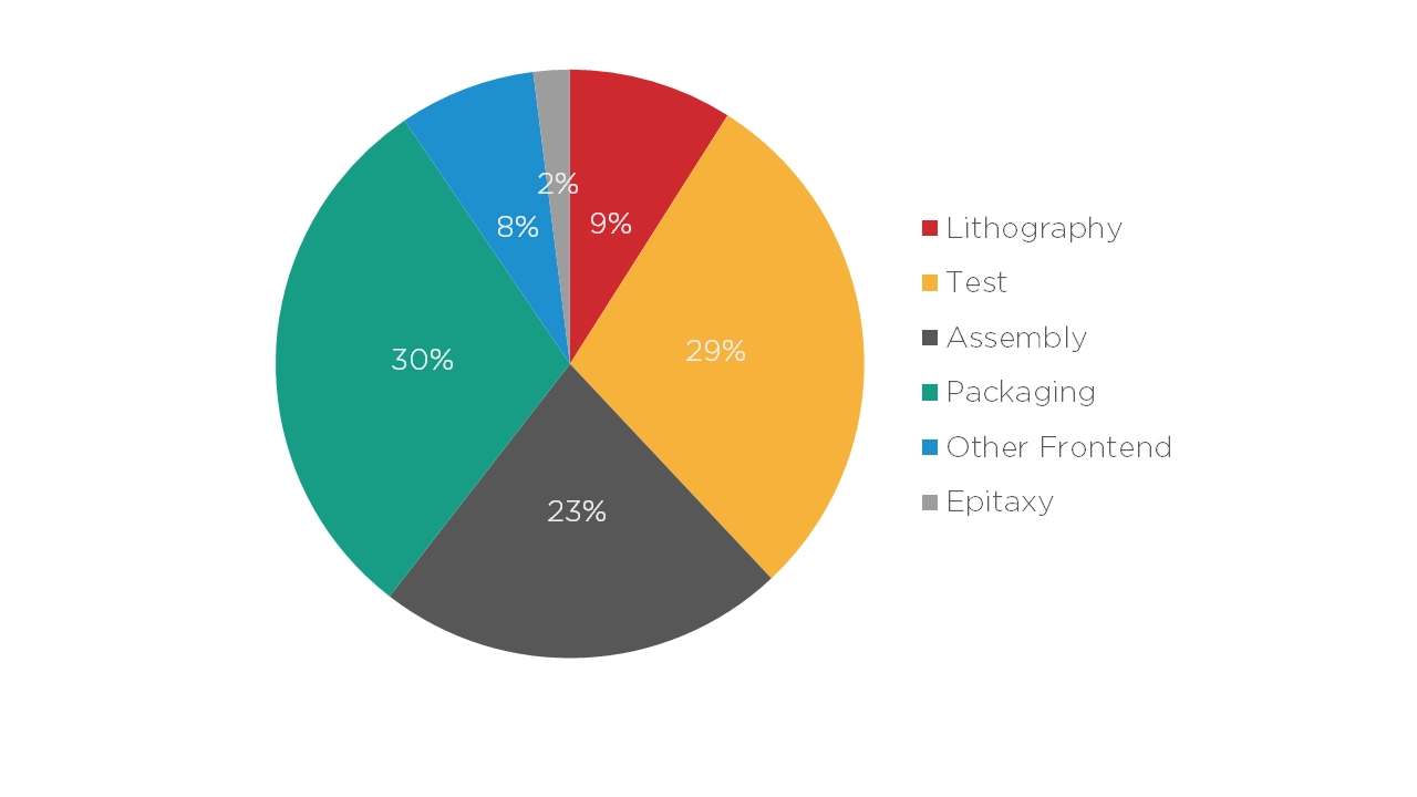
Today, photonics is still a ways off from achieving the goal of becoming more like electronics in its manufacturing process. Photonics manufacturing chains are not at a point where they can quickly produce millions of integrated photonic devices per year. While packaging, assembly, and testing are only a small part of the cost of electronic systems, they are 80% of the total module cost in photonics, as shown in the figure below.
To scale and become more affordable, the photonics manufacturing chains must become more automated and leverage existing electronic packaging, assembly, and testing methods that are already well-known and standardized. Technologies like BGA-style packaging and flip-chip bonding might be novel for photonics developers who started implementing them in the last five or ten years, but electronics embraced these technologies 20 or 30 years ago. Making these techniques more widespread will make a massive difference in photonics’ ability to scale up and become as available as electronics.
The roadmap of scaling integrated photonics and making it more accessible is clear: it must leverage existing electronics manufacturing processes and ecosystems and tap into the same economy-of-scale principles as electronics. Implementing this roadmap, however, requires more investment in photonics. While such high-volume photonics manufacturing demands a higher upfront investment, the resulting high-volume production line will drive down the cost per device and opens them up to a much larger market. That’s the process by which electronics revolutionized the world.
Takeaways
A robust investment is needed to better adapt and integrate microelectronic semiconductor processes into the photonics manufacturing chain to harness the full potential of photonic technologies. Such advancements will not only refine the production scales but also enhance the accessibility and affordability of photonic solutions.
Tags: bandgap, BGA style packaging, Coherent Transceivers, computing power, economy-of-scale principles, EFFECT Photonics, electronic packaging, electronics, Fabless model, Flip-chip bonding, GaAs, high-volume production, III-V semiconductor materials, InP, Investment, lasers, manufacturing chains, microelectronics industry, optical network, Optics, Photodetectors, photonic components, Photonic devices, photonic solutions, Photonics, photonics developers, photonics manufacturing, Semiconductor, semiconductor fabrication techniques, silicon, transistor, wafer-scale technology