Join EFFECT Photonics from April 1 to 3, 2025 at the 50th OFC in San…
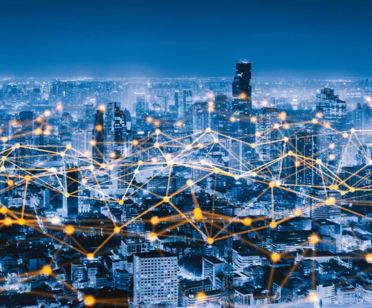
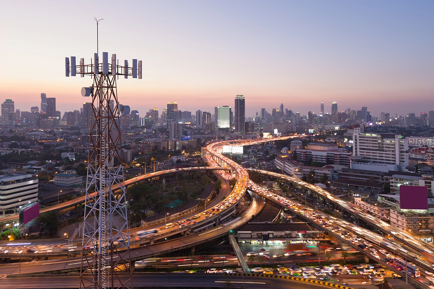
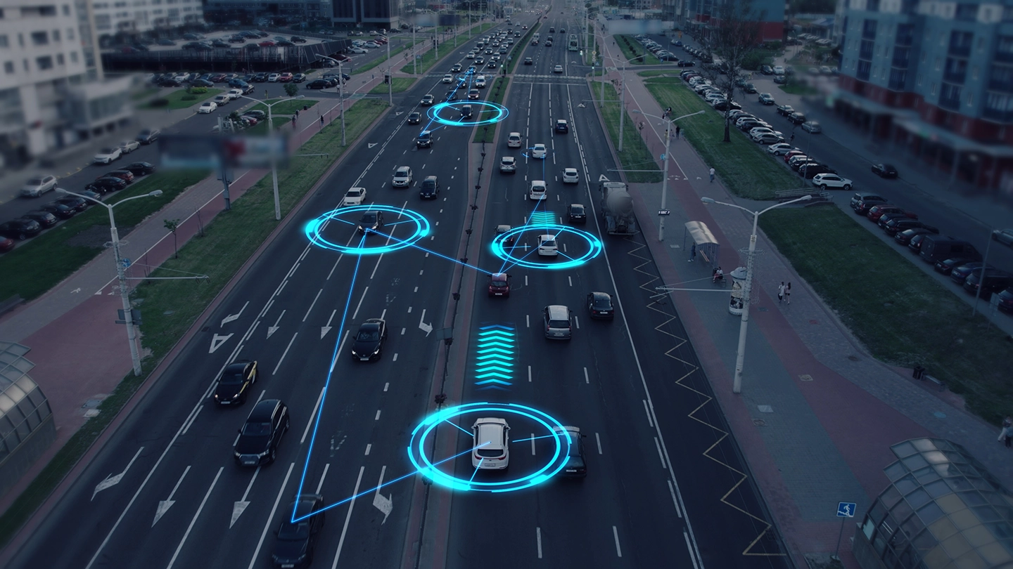
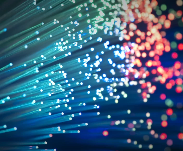
Join EFFECT Photonics from April 1 to 3, 2025 at the 50th OFC in San Francisco, California, the world’s largest event for optical networking and communications, to discover firsthand how our technology is transforming where light meets digital. Visit Booth #2850 to learn how EFFECT Photonics’ full portfolio of optical building blocks are enabling 100G coherent to the network edge and next-generation applications.
What to Expect in 2025:
Global Participation: Anticipate over 13,500 participants from 83+ countries, alongside 670 exhibiting companies, making it a truly international affair.
Innovation Hub: Witness the debut of startups and the pioneering strides of industry leaders, setting the tone for the future of optical communications.
Inclusive Programs: Immerse yourself in a diverse array of programs and events designed to encompass the entire ecosystem, with a strong emphasis on inclusivity.
Key Highlights:
Interoperability Demonstrations: Experience live demonstrations by leading optics companies, showcasing seamless integration over OFCnet.
Plenary Sessions: be inspired by industry luminaries as they delve into the transformative power of technology and its impact on our world.
Tags: 100 ZR, 100G, 100gcoherent, access, access networks, bringing100Gtoedge, cloud, cloudedge, coherent, coherentoptics, datacenters, DSP, DSPs, EFFECT Photonics, Integrated Photonics, networkedge, ofc23, opticcommunications, Optics, photonic integration, Photonics, PIC, tunablelasers, wherelightmeetsdigital