
Transceiver Integration for the Energy Transition
The world relies heavily on traditional fossil fuels like coal, oil, and natural gas, but their environmental impact has prompted a critical reevaluation. The energy transition is a strategic pivot towards cleaner and more sustainable energy sources to reduce carbon emissions.
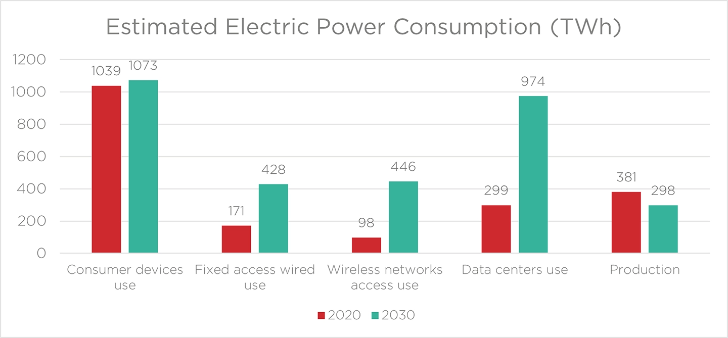
In the information and communication technology (ICT) sector, the exponential increase in data traffic makes it difficult to keep emissions down and contribute to the energy transition. A 2020 study by Huawei estimates that the power consumption of the data center sector will increase threefold in the next ten years. Meanwhile, wireless access networks are expected to increase their power consumption even faster, more than quadrupling between 2020 and 2030.
These issues affect both the environment and the bottom lines of communications companies, which must commit increasingly larger percentages of their operating expenditure to cooling solutions.
As we explained in our previous article, photonics will play a key role in addressing these issues and making the ICT sector greener. However, contributing to a successful energy transition requires more than replacing specific electronic components with photonic ones. Existing photonic components, such as optical transceivers, must also be upgraded to more highly integrated and power-efficient ones. As we will show in this article, even small improvements in existing optical transceivers can snowball into more significant power savings and carbon emissions reduction.
How One Watt of Savings Scales Up
Let’s discuss an example to show how a seemingly small improvement of one watt in pluggable transceiver power consumption can quickly scale up into major energy savings.
A 2020 paper from Microsoft Research estimates that for a metropolitan region of 10 data centers with 16 fiber pairs each and 100-GHz DWDM per fiber, the regional interconnect network needs to host 12,800 transceivers.
This number of transceivers could increase by a third in the coming years since the 400ZR transceiver ecosystem supports a denser 75 GHz DWDM grid, so this number of transceivers would increase to 17,000. Therefore, saving a watt of power in each transceiver would lead to a total of 17 kW in savings.
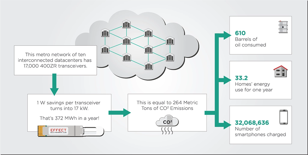
The power savings don’t end there, however. The transceiver is powered by the server, which is then powered by its power supply and, ultimately, the national electricity grid. On average, 2.5 Watts must be supplied from the national grid for every watt of power the transceiver uses. When applying that 2.5 factor, the 17 kW in savings we discussed earlier are, in reality, 42.5 kW.
In a year of power consumption, this rate adds up to a total of 372 MWh in power consumption savings. According to the US Environmental Protection Agency (EPA), these power savings in a single metro data center network are equivalent to 264 metric tons of carbon dioxide emissions. These emissions are equivalent to consuming 610 barrels of oil and could power up to 33 American homes for a year.
Saving Power through Integration
Having explained the potential impact of transceiver power savings, let’s delve into how to save this power.
Before 2020, Apple made its computer processors with discrete components. In other words, electronic components were manufactured on separate chips, and then these chips were assembled into a single package. However, the interconnections between the chips produced losses and incompatibilities that made their devices less energy efficient. After 2020, starting with Apple’s M1 processor, they fully integrated all components on a single chip, avoiding losses and incompatibilities. As shown in the table below, this electronic system-on-chip (SoC) consumes a third of the power compared to the processors with discrete components used in their previous generations of computers.
| 𝗠𝗮𝗰 𝗠𝗶𝗻𝗶 𝗠𝗼𝗱𝗲𝗹 | 𝗣𝗼𝘄𝗲𝗿 𝗖𝗼𝗻𝘀𝘂𝗺𝗽𝘁𝗶𝗼𝗻 | |
| 𝗜𝗱𝗹𝗲 | 𝗠𝗮𝘅 | |
| 2023, M2 | 7 | 5 |
| 2020, M1 | 7 | 39 |
| 2018, Core i7 | 20 | 122 |
| 2014, Core i5 | 6 | 85 |
| 2010, Core 2 Duo | 10 | 85 |
| 2006, Core Solo or Duo | 23 | 110 |
| 2005, PowerPC G4 | 32 | 85 |
| Table 1: Comparing the power consumption of a Mac Mini with an M1 and M2 SoC chips to previous generations of Mac Minis. [Source: Apple’s website] | ||
The photonics industry would benefit from a similar goal: implementing a photonic system-on-chip. Integrating all the required optical functions on a single chip can minimize the losses and make devices such as optical transceivers more efficient.
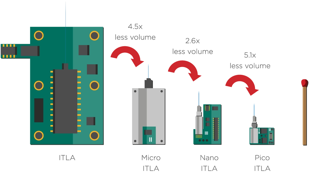
For example, the monolithic integration of all tunable laser functions allows EFFECT Photonics to develop a novel pico-ITLA (pITLA) module that will become the world’s smallest ITLA for coherent optical transceivers. The pITLA is the next step in tunable laser integration, including all laser functions in a package with just 20% of the volume of a nano-ITLA module. This increased integration aims to reduce the power and cost per bit transmitted further.
Early Testing Avoids Wastage
Testing is another aspect of the manufacturing process that impacts sustainability. The earlier faults are found in the testing process, the greater the impact on the materials and energy to process defective chips. Ideally, testing should happen not only on the final, packaged transceiver but also in the earlier stages of PIC fabrication, such as measuring after wafer processing or cutting the wafer into smaller dies.
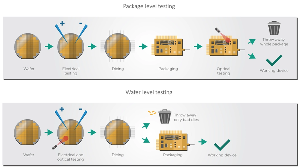
When optical testing is done just on the finalized transceiver package, the whole package must often be discarded, even if just one component does not pass the testing process. This action can lead to a massive waste of materials that cannot be ”fixed” or reused at this stage of the manufacturing process.
Full integration of optical devices enables earlier optical testing on the semiconductor wafer and dies. By testing the dies and wafers directly before packaging, manufacturers need only discard the bad dies rather than the whole package, which saves valuable energy and materials.
Takeaways
For photonics to enable an energy transition in the ICT sector, it must be as accessible and easy to use as electronics. Like electronics, it must be built on a wafer-scale process that can produce millions of chips monthly.
Increased integration of photonic devices such as optical transceivers does not just reduce their energy consumption; it also makes them easier to produce at high volumes. Integrating all functions of an optical device into a single chip makes it much easier to scale up the manufacturing of that device. This scaling will drive down production costs, making integrated photonics more widely available and paving the way for its impactful integration into numerous technologies across the globe.