International growth opportunities for the photonics ecosystem, provided challenges around talent, scale-up and technology are solved
International growth opportunities for the photonics ecosystem, provided challenges around talent, scale-up and technology are solved
Faster, lighter, more durable, and, at the end of the day, also much cheaper: the benefits of photonic circuits are considerable, for a wide range of applications. And the Netherlands plays an important role, globally, in the development and application of this key technology. In recent years, under the leadership of PhotonDelta, a solid foundation has been laid under the Dutch integrated photonics ecosystem. In the final episode of this series, we survey the playing field with Kathleen Philips (imec) and Boudewijn Docter (EFFECT Photonics). Read the whole series here.
Things are going well for the Dutch ecosystem around integrated photonics. Thanks to the perspectives shared by renowned representatives of this rapidly emerging industry in this series of articles, we learned that an international breakthrough is just around the corner. Obviously, this won’t be possible without a lot of investments. But in addition to that, general manager Kathleen Philips of imec at Holst Centre, three factors are all-important: choosing the right technology, growing into an ‘economy of scale’, and talent.
Imec’s headquarters are in Leuven; in the Netherlands, the renowned research institute is based in Eindhoven (as part of Holst Centre on the High Tech Campus) and Wageningen (with the OnePlanet Research Center). Although the Netherlands is primarily committed to Indium Phosphide (InP) and Silicon Nitride (SiN) production platforms, Kathleen Philips would like to make a case for internationalizing by joining CMOS-based work platforms such as Silicon Photonics (SiPh). “It offers the best opportunities for international support and that is essential for our growth ambitions.”
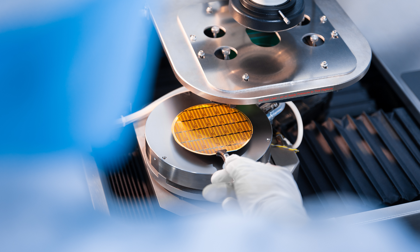
| What is (integrated) photonics? Photonics is similar to electronics. However, instead of electrons, it uses photons (light) to transmit information. Photonic technology detects, generates, transports, and processes light. Current applications include solar cells, sensors, and fiber-optic networks. Photonic chips, officially called Photonic Integrated Circuits (PICs), integrate various photonic and often electronic functions into a microchip to make smaller, faster, and more energy-efficient devices. Because they are manufactured like traditional chips (with wafer-scale technology), mass production is also within reach – with price drop as a result. More here. |
At imec, Kathleen Philips has an excellent overview of the status of photonics developments in the Netherlands and Belgium. She is thus able to combine the Dutch emphasis on Indium Phosphide and Silicon Nitride with the ‘Leuven’ expertise on Silicon Photonics. “We must be careful not to operate in ‘splendid isolation’. It is precisely in the hybrid combination of platforms that we find the desired connection to the world stage. Moreover, silicon photonics is largely compatible with classical and mainstream CMOS chip production lines, the value of which should never be underestimated. That said; if you need good lasers or low-loss waveguides, then InP and SiN platforms are an essential complement.”
Top-Notch
The next step is in creating an economy of scale, says Philips. “High volume is needed to lower the price of the end product. This automatically means you have to look across borders. Even a European scale is insufficient in that respect; we also have to focus on America and Asia. In photonics, you see the same development as in the semiconductor industry: the promise lies in the high volumes. We know that by scaling up the price goes down.”
The Netherlands has everything it needs to make that leap, Philips emphasizes. “You have to be top-notch to make an impact worldwide. And fortunately, we are. Our R&D is renowned, also historically. We are excellently positioned to connect with the big American flagships, for example. With Eindhoven, Twente and Delft we have academic gems. Their research, their publications, their professors, but also the rich ecosystem of start-ups around them and of course Photondelta: it’s all exactly how we would want to see it. Combine that with the presence of a solid high tech industry with major corporations such as ASML and NXP, and institutes like TNO and imec, and you know that a lot of good things are awaiting us.”
But, Philips warns, “to be successful we must be prepared to look beyond the important Dutch photonics industry and also strategically align ourselves internationally. In particular, the Dutch-Flemish axis offers wonderful opportunities and imec can play a connecting role. From Holst Centre in Eindhoven, we work closely with all the Dutch representatives of the ecosystem. Our colleagues in Leuven have strong international roots, with complementary technology and knowledge.” What helps, she adds, is that both at the Dutch and European level the realization has sunk in that governments can also help financially in this regard. Imec already makes use of Interreg subsidies, but the EU Chips Act is also full of promise in this regard. “And at a national level, there is a chance that the photonics sector can make use of the funding that is going to be distributed through the National Growth Fund. In short: there is much more awareness than before that public investment is important here.”
Talent
In a growth market, finding sufficient talent is always a challenge. In the photonics industry, it is no different. There is no shortage of good universities, says Philips. She mentions the three Dutch Universities of Technology, as well as those of Ghent, Leuven, and Brussels as important centers of expertise. “But you also need crown jewels: companies that capture the imagination so much that they manage to attract the best people, wherever they come from.” As an example, she points to EFFECT Photonics, founded in Eindhoven but grown – in a relatively short time – into a scale-up with some 250 people and offices around the world. “With that, EFFECT also shows how important scaling up is; not just for the company itself, but for our entire ecosystem.”
Indeed, the increasing awareness of EFFECT’s achievements has resulted in more talents knocking on their door. “But in addition to that, we also reach out to the talents ourselves,” adds founder Boudewijn Docter. “In fact, that’s one of the main reasons for our recent acquisition in the United States. We see that young people from all over the world have no trouble finding their way to Eindhoven. Recent graduates and PhDs, for example. They are very important, but we also need more experienced people and for them, it is often more difficult to leave hearth and home for a new workplace on the other side of the world.” And yet it is precisely those people who are desperately needed, Docter says. “The most important engineering skills can only be learned in practice. For the phase in which we are now, trial and error is no longer enough – we also need solid experience.”
This desire to hire more experienced people also leads to more remote work. “But even then, we would like people to come to Eindhoven from time to time, especially if they are working on multidisciplinary projects.” The best is a mix of young and experienced, in-house and remote. “With such a mix, young people find the best circumstances to grow, because they can take an example from their colleagues with a bit more experience.”
Volume
Docter is convinced that the choice to locate EFFECT’s business in places where the talent can be found ultimately also offers advantages for the Netherlands. “By growing all over the world, we become more visible as part of the national and European ecosystem. That in itself then attracts new talent, allowing the entire industry to grow.” This, in turn, is beneficial for this economy of scale also desired by Kathleen Philips. “In the semiconductor industry you always need volume”, Docter also says. “Because only then do you really start to notice the advantages. You have to know which markets you want to work for. For example, do you opt for a flexible design of your device, or a very specific one? Either way, you need to improve and stabilize your manufacturing process, which consists of hundreds of steps. Each step must deliver a 99.9999% yield, but it takes time to get there. Not only for us, by the way, but for all stakeholders in our industry, even the biggest ones. We have not yet built up sufficient experience for ‘First Time Right’, with the reliability that goes with such an ambition, but partly due to the focus on volume, we are already very well on our way to maturity.”
The imec model
Kathleen Philips is pleased that imec can play an important role in this global development. “The imec model, in which we set up R&D programs with various partners in a precompetitive setting, and our emphasis on the integration of different production platforms are essential. We are that neutral zone within which you can technically try out new ideas, and test a prototype in the value chain with limited costs. Sometimes this leads to the creation of new start-ups, or to collaboration with existing parties. But always it creates new or stronger ecosystems that the entire industry can benefit from.”