
From the Lab Boutique to High Volume Production: How to Scale Up Photonics Manufacturing
Photonics, the science and technology of generating, detecting, and manipulating light, has witnessed remarkable progress in recent years. From cutting-edge research in academic labs to breakthrough innovations in startups, photonics is poised to revolutionize various industries, from telecommunications to healthcare. However, despite its tremendous potential, the transition from boutique lab-scale production to high-volume manufacturing remains a significant challenge.
To overcome this hurdle, the photonics industry must draw lessons from the successful scaling of electronics manufacturing. By adopting key strategies and practices that have propelled the electronics industry into the realm of mass production, photonics can pave the way for widespread adoption and integration into our everyday lives.
Learning from Electronics Packaging
A key way to improve photonics manufacturing is to learn from electronics packaging, assembly, and testing methods that are already well-known and standardized. After all, building a new special production line is much more expensive than modifying an existing production flow.
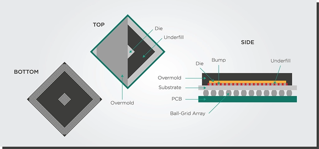
One electronic technique essential to transfer into photonics is ball-grid array (BGA) packaging. BGA-style packaging has grown popular among electronics manufacturers over the last few decades. It places the chip connections under the chip package, allowing more efficient use of space in circuit boards, a smaller package size, and better soldering.
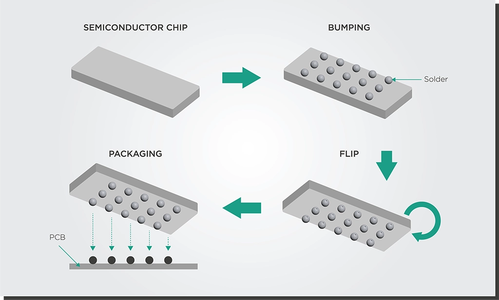
Another critical technique to move into photonics is flip-chip bonding. This process is where solder bumps are deposited on the chip in the final fabrication step. The chip is flipped over and aligned with a circuit board for easier soldering.
These might be novel technologies for photonics developers who have started implementing them in the last five or ten years. However, the electronics industry embraced these technologies 20 or 30 years ago. Making these techniques more widespread will make a massive difference in photonics’ ability to scale up and become as available as electronics.
Adopting BGA-style packaging and flip-chip bonding techniques will make it easier for PICs to survive this soldering process. There is ongoing research and development worldwide, including at EFFECT Photonics, to transfer more electronics packaging methods into photonics. PICs that can handle being soldered to circuit boards allow the industry to build optical subassemblies that are more accessible to the open market and can go into trains, cars, or airplanes.
Supply Chain Optimization
Electronics manufacturers have honed the art of supply chain management to achieve cost-effective and efficient production processes. This includes strategies like just-in-time inventory management, lean manufacturing principles, and global sourcing. In contrast, the photonics industry often faces challenges related to specialized materials and components, resulting in longer lead times and higher costs.
Photonics manufacturers can learn from electronics by implementing supply chain optimization strategies. This involves diversifying sources, streamlining production workflows, and leveraging economies of scale. By fostering strategic partnerships with suppliers and embracing advanced inventory management systems, the photonics industry can overcome the hurdles that have hindered its growth.
The Advantages of Moving to a Fabless Model
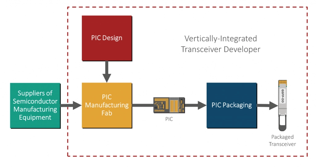
Increasing the volume of photonics manufacturing is a big challenge. Some photonic chip developers manufacture their chips in-house within their fabrication facilities. This approach has some substantial advantages, giving component manufacturers complete control over their production process.
However, if a vertically-integrated chip developer wants to scale up in volume, they must make a hefty capital expenditure (CAPEX) in more equipment and personnel. They must develop new fabrication processes as well as develop and train personnel. Fabs are not only expensive to build but to operate. Unless they can be kept at nearly full utilization, operating expenses (OPEX) also drain the facility owners’ finances.
Especially in the case of an optical transceiver market that is not as big as that of consumer electronics, it’s hard not to wonder whether that initial investment is cost-effective. For example, LightCounting estimates that 55 million optical transceivers were sold in 2021, while the International Data Corporation estimates that 1.4 billion smartphones were sold in 2021. The latter figure is 25 times larger than that of the transceiver market.
Electronics manufacturing experienced a similar problem during their 70s and 80s boom, with smaller chip start-ups facing almost insurmountable barriers to market entry because of the massive CAPEX required. Furthermore, the large-scale electronics manufacturing foundries had excess production capacity that drained their OPEX. The large-scale foundries ended up selling that excess capacity to the smaller chip developers, who became fabless. In this scenario, everyone ended up winning. The foundries serviced multiple companies and could run their facilities at total capacity, while the fabless companies could outsource manufacturing and reduce their expenditures.
This fabless model, with companies designing and selling the chips but outsourcing the manufacturing, could also be the way to go for photonics. The troubles of scaling up for photonics developers are outsourced and (from the perspective of the fabless company) become as simple as putting a purchase order in place. Furthermore, the fabless model allows photonics developers to concentrate their R&D resources on the end market. This might be the most straightforward way for photonics to move into million-scale volumes.
Takeaways
Scaling up photonics manufacturing from boutique labs to high-volume production is a pivotal step in realizing the full potential of this transformative technology. By taking a page from the electronics industry’s playbook, focusing on standardization, optimizing the supply chain, and embracing automation, the photonics industry can overcome the challenges that have impeded its growth. With concerted efforts and strategic investments, the future of photonics looks poised for a paradigm shift, bringing us closer to a world illuminated by the power of light.