
How to Test a Photonic Integrated Circuit
As photonic integrated circuits (PICs) continue to play an increasingly vital role in modern communication systems, understanding their testing process is crucial to ensure their reliability and performance. Chip fabrication is a process with many sources of variability, and therefore, much testing is required to ensure that the fabricated chip agrees with what was originally designed and simulated.
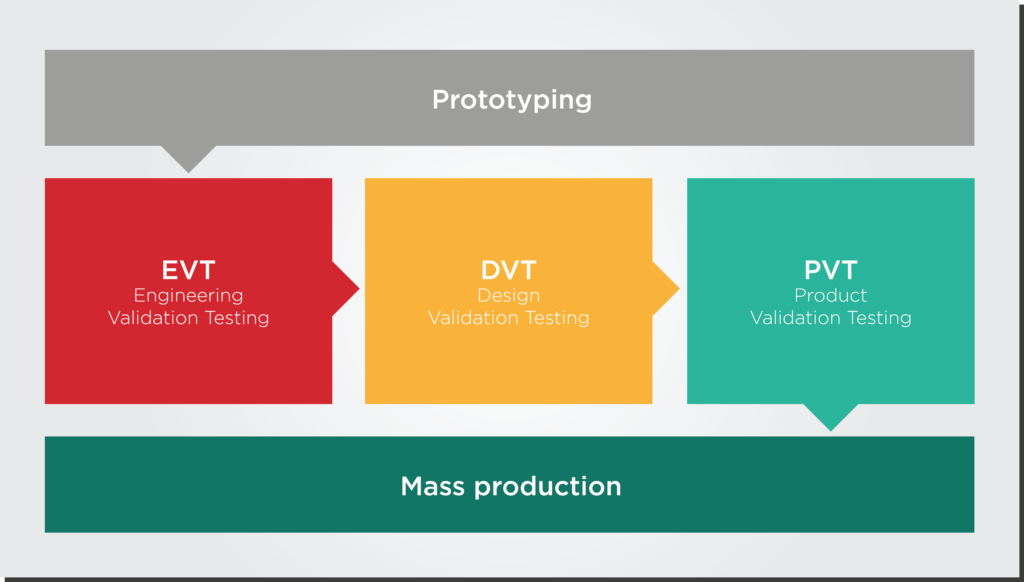
As with most hardware, PIC testing can follow the steps of the DVT/EVT/PVT validation framework to scale the device from a mere prototype to a stage of mass production.
- EVT (Engineering Validation Test): This is the initial phase of hardware testing, where the focus is on validating that the engineering design meets the specifications and requirements.
- DVT (Design Validation Test): This phase aims to ensure that the hardware design is mature and stable, ready for production.
- PVT (Production Validation Test): PVT is conducted using production-intent materials and processes to verify that the final product will meet quality and performance expectations in mass production.
This article aims to provide an overview of some testing processes for photonic integrated circuits, covering device-level testing, functional testing, and reliability testing.
Device Level Testing
Device-level testing involves evaluating individual components within the PIC and assessing their characteristics, performance, and reliability to ensure proper functionality and integration. This testing is typically performed at the chip level or wafer level.
Ideally, testing should happen not only on the final, packaged device but in the earlier stages of PIC fabrication, such as measuring after the wafer fabrication process is completed or after cutting the wafer into smaller dies.
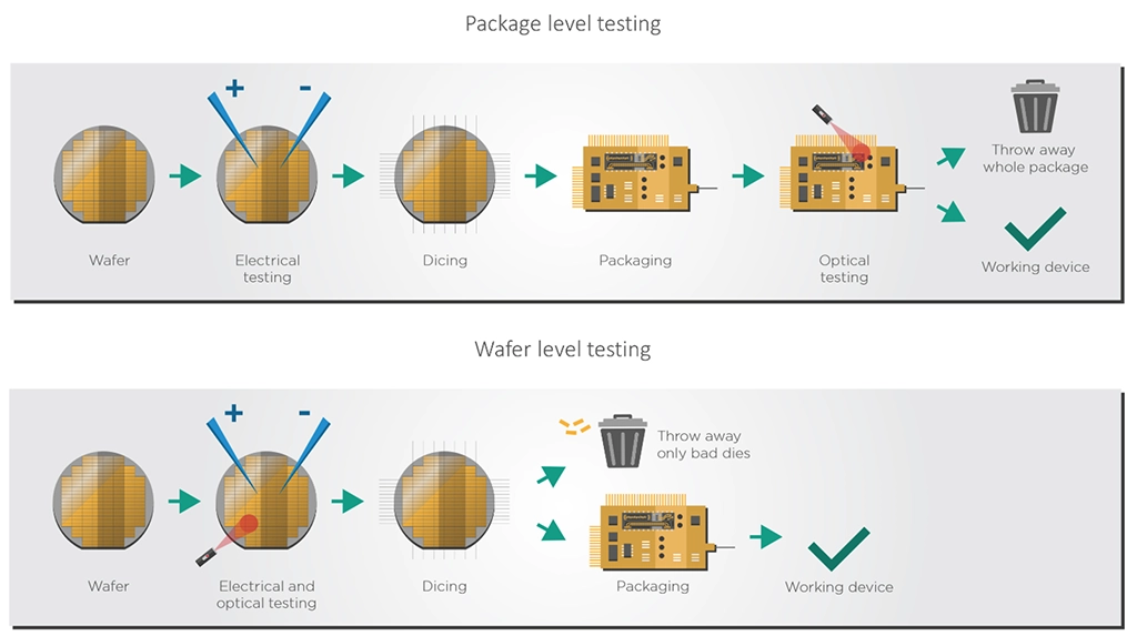
Greater integration of the PICs enables earlier optical testing on the semiconductor wafer and dies. By testing the dies and wafers directly before packaging, manufacturers need only discard the bad die rather than the whole package, which saves valuable energy and materials.
Functional Testing
After the individual device testing, the next step of the EVT testing phase is functional testing. These tests evaluate the key functionalities of the PIC to ensure they meet design specifications and goals. Different applications will have different functionalities to be evaluated, of course. For example, some key functions evaluated in a PIC for telecommunications can be:
- Signal Transmission: To ensure reliable transmission, evaluate signal quality, bit error rate, and signal-to-noise ratio.
- Modulation: Assessing the modulators’ accuracy, bandwidth, and linearity to ensure accurate signal encoding and decoding.
- Switching: Evaluate the switch response time, crosstalk, and extinction ratio to ensure proper signal routing and minimal signal degradation.
Reliability Testing of the Packaged PIC
After the EVT round of characterization and validation of the chip and its package, the packed chip must be made ready for production, requiring a series of reliability tests in several environmental conditions. For example, different applications need different certifications of the temperatures in which the chip must operate.
For example, the packaged PICs made by EFFECT Photonics for telecommunications must comply with the Telcordia GR-468 qualification, which describes how to test optoelectronic devices for reliability under extreme conditions. Qualification depends upon maintaining optical integrity throughout an appropriate test regimen. Accelerated environmental tests are described in the diagram below.
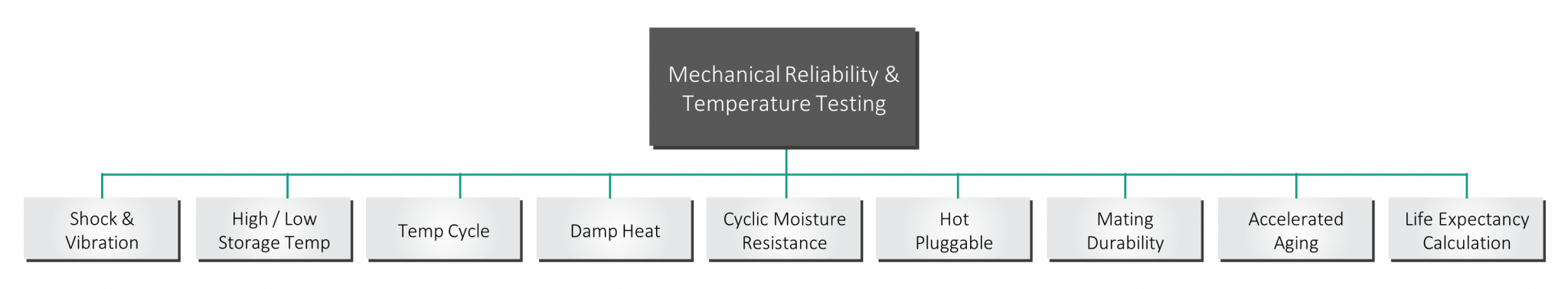
Our testing facilities and partners include capabilities for the temperature cycling and reliability testing needed to match Telcordia standards, such as temperature cycling ovens and chambers with humidity control.
Takeaways
The testing process for photonic integrated circuits ensures their reliability and performance. Device-level testing focuses on individual components, allowing for precise characterization and identification of faulty elements. Functional testing evaluates the overall performance of the PIC, ensuring adherence to design specifications. Reliability testing assesses the robustness and lifespan of the PIC under various operating conditions.