– 5G TechnologyWorld

– 5G TechnologyWorld

Join EFFECT Photonics from March 7 to 9, 2023 at OFC in San Diego, California, the world’s largest event for optical networking and communications, to discover firsthand how our technology is transforming where light meets digital. Visit Booth #2423 to learn how EFFECT Photonics’ full portfolio of optical building blocks are enabling 100G coherent to the network edge and next-generation applications.
Build Your Own 100G ZR Coherent Module
At this year’s OFC, see how easy and affordable it can be to upgrade existing 10G links to a more scalable 100G coherent solution! Try your hand at constructing a 100G ZR coherent module specifically designed for the network edge utilizing various optical building blocks including tunable lasers, DSPs and optical subassemblies.
Tune Your Own PIC (Photonic Integrated Circuit)
Be sure to stop by Booth #2423 to tune your own PIC with EFFECT Photonics technology. In this interactive and dynamic demonstration, participants can explore first-hand the power of EFFECT Photonics solutions utilizing various parameters and product configurations.
Our experts are also available to discuss customer needs and how EFFECT Photonics might be able to assist. To schedule a meeting, please email marketing@effectphotonics.com
Tags: 100 ZR, 100G, 100gcoherent, access, access networks, bringing100Gtoedge, cloud, cloudedge, coherent, coherentoptics, datacenters, DSP, DSPs, EFFECT Photonics, Integrated Photonics, networkedge, ofc23, opticcommunications, Optics, photonic integration, Photonics, PIC, tunablelasers, wherelightmeetsdigital
-New pTLA to offer industry-best combination of size, affordability, and performance to meet the demand…
-New pTLA to offer industry-best combination of size, affordability, and performance to meet the demand for 100G coherent at the edge
EFFECT Photonics, a leading developer of highly integrated optical solutions, announced today the development of a new Pico Tunable Laser Assembly (pTLA) to address the growing demand for 100G coherent transceivers in access networks. Tunable lasers are a core component of optical systems enabling dense wavelength division multiplexing (DWDM) which allows network operators to expand their network capacity without expanding the existing fiber infrastructure. Purposely designed for the optical network edge, EFFECT Photonics new pTLA supports both commercial- and industrial-temperature (C-temp and I-temp) operating ranges and offers an ideal combination of power, cost, and size to enable a transceiver form-factors to upgrade the existing infrastructure to a scalable 100 Gbps coherent solution.
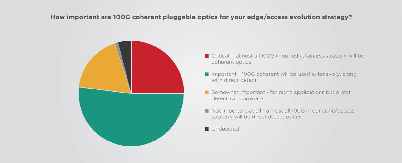
According to a recent Heavy Reading survey, 75% of operators believe that 100G coherent pluggable optics will be used extensively in their edge and access evolution strategy. However, market adoption has yet to materialize since affordable and power-efficient 100ZR-based products are currently not available due to stringent size and power consumption requirements that cannot be fulfilled by today’s tunable laser solutions. Designed specifically to address the 100G coherent network edge, EFFECT Photonics’ pTLA will allow coherent pluggables to be deployed more easily and cost effectively in the access domain and will feature optimal laser performance, size and power consumption for a standard QSFP28 form-factor. Furthermore, EFFECT Photonics’ new pTLA utilizes the existing microelectronics ecosystem to allow manufacturing at scale as well as complementary coherent products and services, such as DSPs for those providers in need of a complete transceiver solution.
Today’s operators need an network edge aggregation strategy that offers the best combination of capacity, cost-effectiveness, and performance to evolve network access effectively, and 100G coherent pluggable optics offer just that, EFFECT Photonics’ new Pico Tunable Laser Assembly will be the only purpose designed tunable laser assembly today to serve this emerging market. helping to easily scale up network edge aggregation capacity and benefit from coherent technology.
Roberto Marcoccia, CEO, EFFECT Photonics
Where Light Meets Digital – EFFECT Photonics is a highly vertically integrated, independent optical systems company addressing the need for high-performance, affordable optic solutions driven by the ever-increasing demand for bandwidth and faster data transfer capabilities.
Using our proprietary digital signal processing and forward error correction technology and ultra-pure light sources, we offer compact form factors with seamless integration, cost efficiency, low power, and security of supply. By leveraging established microelectronics ecosystems, we aim to make our products affordable and available in high volumes to address the challenges in 5G and beyond, access-ready coherent solutions, and cloud and cloud edge services.
For more information, please visit: www.effectphotonics.com. Follow EFFECT Photonics on LinkedIn and Twitter.
To read the Simplified Chinese version click here.
To read the Traditional Chinese version click here.
To read the Japanese version click here.
To read the Korean version click here.
To read the English version click here.
# # #
Media Contact:
Colleen Cronin
EFFECT Photonics
colleencronin@effectphotonics.com

In the optical access networks, the 400ZR pluggables that have become mainstream in datacom applications…
In the optical access networks, the 400ZR pluggables that have become mainstream in datacom applications are too expensive and power-hungry. Therefore, operators are strongly interested in 100G pluggables that can house coherent optics in compact form factors, just like 400ZR pluggables do. The industry is labeling these pluggables as 100ZR.
A recently released Heavy Reading survey revealed that over 75% of operators surveyed believe that 100G coherent pluggable optics will be used extensively in their edge and access evolution strategy. However, this interest had yet to materialize into a 100ZR market because no affordable or power-efficient products were available. The most the industry could offer was 400ZR pluggables that were “powered-down” for 100G capacity.
By embracing smaller and more customizable light sources, new optimized DSP designs, and high-volume manufacturing capabilities, we can develop native 100ZR solutions with lower costs that better fit edge and access networks.
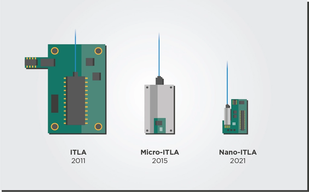
Since the telecom and datacom industries want to pack more and more transceivers on a single router faceplate, integrable tunable laser assemblies (ITLAs) must maintain performance while moving to smaller footprints and lower power consumption and cost.
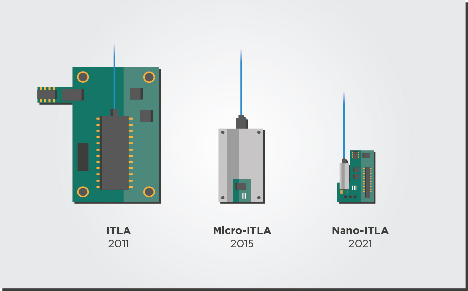
Fortunately, such ambitious specifications became possible thanks to improved photonic integration technology. The original 2011 ITLA standard from the Optical Internetworking Forum (OIF) was 74mm long by 30.5mm wide. By 2015, most tunable lasers shipped in a micro-ITLA form factor that cut the original ITLA footprint in half. In 2021, the nano-ITLA form factor designed for QSFP-DD and OSFP modules had once again cut the micro-ITLA footprint almost in half.
There are still plenty of discussions over the future of ITLA packaging to fit the QSFP28 form factors of these new 100ZR transceivers. For example, every tunable laser needs a wavelength locker component that stabilizes the laser’s output regardless of environmental conditions such as temperature. Integrating that wavelength locker component with the laser chip would help reduce the laser package’s footprint.
Another potential future to reduce the size of tunable laser packages is related to the control electronics. The current ITLA standards include the complete control electronics on the laser package, including power conversion and temperature control. However, if the transceiver’s main board handles some of these electronic functions instead of the laser package, the size of the laser package can be reduced.
This approach means that the reduced laser package would only have full functionality if connected to the main transceiver board. However, some transceiver developers will appreciate the laser package reduction and the extra freedom to provide their own laser control electronics.
The 5 Watt-power requirement of 100ZR in a QSFP28 form factor is significantly reduced compared to the 15-Watt specification of 400ZR transceivers in a QSFP-DD form factor. Achieving this reduction requires a digital signal processor (DSP) specifically optimized for the 100G transceiver.
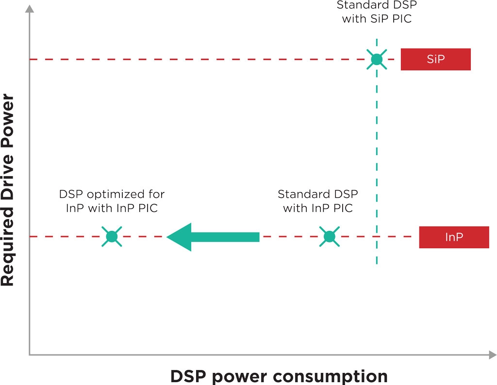
Current DSPs are designed to be agnostic to the material platform of the photonic integrated circuit (PIC) they are connected to, which can be Indium Phosphide (InP) or Silicon. Thus, they do not exploit the intrinsic advantages of these material platforms. Co-designing the DSP chip alongside the PIC can lead to a much better fit between these components.
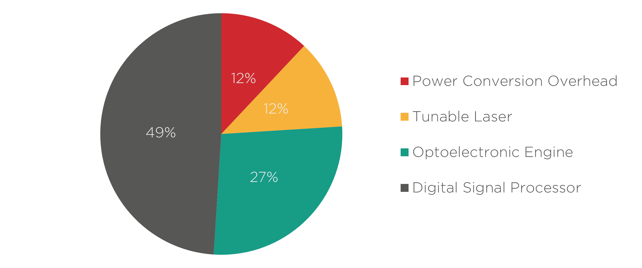
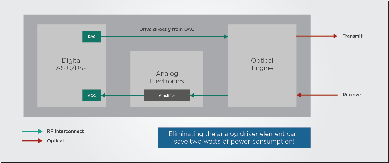
To illustrate the impact of co-designing PIC and DSP, let’s look at an example. A PIC and a standard platform-agnostic DSP typically operate with signals of differing intensities, so they need some RF analog electronic components to “talk” to each other. This signal power conversion overhead constitutes roughly 2-3 Watts or about 10-15% of transceiver power consumption.
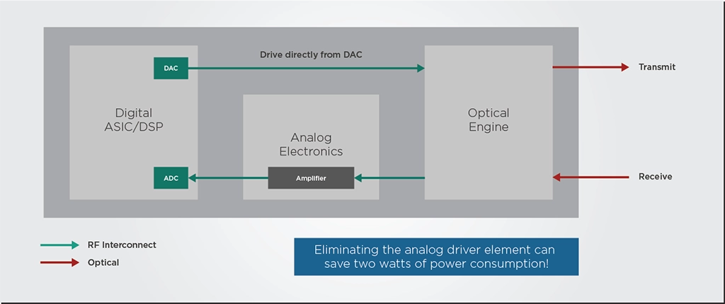
However, the modulator of an InP PIC can run at a lower voltage than a silicon modulator. If this InP PIC and the DSP are designed and optimized together instead of using a standard DSP, the PIC could be designed to run at a voltage compatible with the DSP’s signal output. This way, the optimized DSP could drive the PIC directly without needing the RF analog driver, doing away with most of the power conversion overhead we discussed previously.
To become more accessible and affordable, the photonics manufacturing chain can learn from electronics packaging, assembly, and testing methods that are already well-known and standardized. After all, building a special production line is much more expensive than modifying an existing production flow.
There are several ways in which photonics packaging, assembly, and testing can be made more affordable and accessible: passive alignments of the optical fiber, BGA-style packaging, and flip-chip bonding. Making these techniques more widespread will make a massive difference in photonics’ ability to scale up and become as available as electronics. To read more about them, please read our previous article.
The interest in novel 100ZR coherent pluggable optics for edge and access applications is strong, but the market has struggled to provide “native” and specific 100ZR solutions to address this interest. Transceiver developers need to embrace several new technological approaches to develop these solutions. They will need smaller tunable laser packages that can fit the QSFP28 form factors of 100ZR solutions, optimized and co-designed DSPs that meet the reduced power consumption goals, and sub-assemblies that leverage electronic ecosystems for increased scale and reduced cost.
Tags: 100 ZR, 100G, 100ZR, 400ZR, C-band, C-PON, coherent, DSP, filters, future proof, Korea, laser sources, O-band, Packaging, pluggable, roadmap, S-band
In June 2022, transceiver developer II‐VI Incorporated (now Coherent Corp.) and optical networking solutions provider…
In June 2022, transceiver developer II‐VI Incorporated (now Coherent Corp.) and optical networking solutions provider ADVA announced the launch of the industry’s first 100ZR pluggable coherent transceiver. Discussions in the telecom sector about a future beyond 400G coherent technology have usually focused on 800G products, but there is increasing excitement about “downscaling” to 100G coherent products for certain applications in the network edge and business services. This article will discuss the market and technology forces that drive this change in discourse.
The 400ZR pluggables that have become mainstream in datacom applications are too expensive and power-hungry for the optical network edge. Therefore, operators are strongly interested in 100G pluggables that can house coherent optics in compact form factors, just like 400ZR pluggables do. The industry is labeling these pluggables as 100ZR.
A recently released Heavy Reading survey revealed that over 75% of operators surveyed believe that 100G coherent pluggable optics will be used extensively in their edge and access evolution strategy. However, this interest had not really materialized into a 100ZR market because no affordable or power-efficient products were available. The most the industry could offer was 400ZR pluggables that were “powered-down” for 100G capacity.
With the recent II-VI Incorporated and ADVA announcement, the industry is showing its first attempts at a native 100ZR solution that can provide a true alternative to the powered-down 400ZR products. Some of the key specifications of this novel 100ZR solution include:
The 5 Watt-power requirement is a major reduction compared to the 15-Watt specification of 400ZR transceivers in the QSFP-DD form factor. Achieving this spec requires a digital signal processor (DSP) that is specifically optimized for the 100G transceiver.
Transceiver developers often source their DSP, laser, and optical engine from different suppliers, so all these chips are designed separately from each other. This setup reduces the time to market, simplifies the research and design processes, but comes with performance and power consumption trade-offs.
In such cases, the DSP is like a Swiss army knife: a jack of all trades designed for different kinds of optical engines but a master of none. DSPs co-designed and optimized for their specific optical engine and laser can significantly improve power efficiency. You can read more about co-design approaches in one of our previous articles.
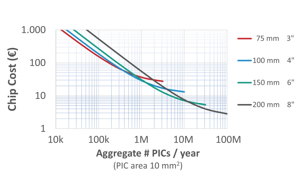
Making 100ZR coherent optical transceivers more affordable is also a matter of volume production. As discussed in a previous article, if PIC production volumes can increase from a few thousand chips per year to a few million, the price per optical chip can decrease from thousands of Euros to mere tens of Euros. Such manufacturing scale demands a higher upfront investment, but the result is a more accessible product that more customers can purchase.
Achieving this production goal requires photonics manufacturing chains to learn from electronics and leverage existing electronics manufacturing processes and ecosystems. Furthermore, transceiver developers must look for trusted large-scale manufacturing partners to guarantee a secure and high-volume supply of chips and packages.
If you want to know more about how photonics developers can leverage electronic ecosystems and methods, we recommend you read our in-depth piece on the subject.
As the Heavy Reading survey showed, the interest in 100G coherent pluggable optics for edge/access applications is strong, and operators have identified use key use cases within their networks. In the past, there were no true 100ZR solutions that could address this interest, but the use of optimized DSPs and light sources, as well as high-volume manufacturing capabilities, can finally deliver a viable and affordable 100ZR product.
Tags: 100G coherent, 100ZR, DSP, DSPs, edge and access applications, EFFECT Photonics, Photonics
Over the last two decades, power ratings for pluggable modules have increased as we moved…
Over the last two decades, power ratings for pluggable modules have increased as we moved from direct detection to more power-hungry coherent transmission: from 2W for SFP modules to 3.5 W for QSFP modules and now to 14W for QSSFP-DD and 21.1W for OSFP form factors. Rockley Photonics researchers estimate that a future electronic switch filled with 800G modules would draw around 1 kW of power just for the optical modules.
Around 50% of a coherent transceiver’s power consumption goes into the digital signal processing (DSP) chip that also performs the functions of clock data recovery (CDR), optical-electrical gear-boxing, and lane switching. Scaling to higher bandwidths leads to even more losses and energy consumption from the DSP chip and its radiofrequency (RF) interconnects with the optical engine.
One way to reduce transceiver power consumption requires designing DSPs that take advantage of the material platform of their optical engine. In this article, we will elaborate on what that means for the Indium Phosphide platform.
Transceiver developers often source their DSP, laser, and optical engine from different suppliers, so all these chips are designed separately from each other. This setup reduces the time to market and simplifies the research and design processes but comes with trade-offs in performance and power consumption.
In such cases, the DSP is like a Swiss army knife: a jack of all trades designed for different kinds of optical engines but a master of none. For example, current DSPs are designed to be agnostic to the material platform of the photonic integrated circuit (PIC) they are connected to, which can be Indium Phosphide (InP) or Silicon. Thus, they do not exploit the intrinsic advantages of these material platforms. Co-designing the DSP chip alongside the PIC can lead to a much better fit between these components.
To illustrate the impact of co-designing PIC and DSP, let’s look at an example. A PIC and a standard platform-agnostic DSP typically operate with signals of differing intensities, so they need some RF analog electronic components to “talk” to each other. This signal power conversion overhead constitutes roughly 2-3 Watts or about 10-15% of transceiver power consumption.
However, the modulator of an InP PIC can run at a lower voltage than a silicon modulator. If this InP PIC and the DSP are designed and optimized together instead of using a standard DSP, the PIC could be designed to run at a voltage compatible with the DSP’s signal output. This way, the optimized DSP could drive the PIC directly without needing the RF analog driver, doing away with most of the power conversion overhead we discussed previously.

Additionally, the optimized DSP could also be programmed to do some additional signal conditioning that minimizes the nonlinear optical effects of the InP material, which can reduce noise and improve performance.
Russell Fuerst, EFFECT Photonics’ Vice-President of Digital Signal Processing, gave us an interesting insight about designing for the InP platform in a previous interview:
When we started doing coherent DSP designs for optical communication over a decade ago, we pulled many solutions from the RF wireless and satellite communications space into our initial designs. Still, we couldn’t bring all those solutions to the optical markets.
However, when you get more of the InP active components involved, some of those solutions can finally be brought over and utilized. They were not used before in our designs for silicon photonics because silicon is not an active medium and lacked the performance to exploit these advanced techniques.
For example, the fact that the DSP could control laser and modulator components on the InP can lead to some interesting manipulations of light signals. A DSP that can control these components directly could generate proprietary waveforms or use non-standard constellation and modulation schemes that can boost the performance of a coherent transceiver and increase the capacity of the link.
The biggest problem for DSP designers is still improving performance while reducing power use. This problem can be solved by finding ways to integrate the DSP more deeply with the InP platform, such as letting the DSP control the laser and modulator directly to develop new waveform shaping and modulation schemes. Because the InP platforms have active components, DSP designers can also import more solutions from the RF wireless space.
Tags: analog electronics, building blocks, coherent, dispersion compensation, DSP, energy efficiency, Intra DCI, Photonics, PON, power consumption, reach, simplified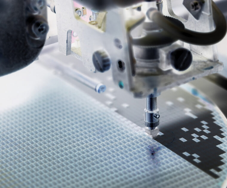
Photonics is one of the enabling technologies of the future. Light is the fastest information…
Photonics is one of the enabling technologies of the future. Light is the fastest information carrier in the universe and can transmit this information while dissipating less heat and energy than electrical signals. Thus, photonics can dramatically increase the speed, reach, and flexibility of communication networks and cope with the ever-growing demand for more data. And it will do so at a lower energy cost, decreasing the Internet’s carbon footprint. Meanwhile, fast and efficient photonic signals have massive potential for sensing and imaging applications in medical devices, automotive LIDAR, agricultural and food diagnostics, and more.
Given its importance, we want to explain how photonic integrated circuits (PICs), the devices that enable all these applications, are made.
The process of designing a PIC should translate an initial application concept into a functioning photonics chip that can be manufactured. In a short course at the OFC 2018 conference, Wim Bogaerts from Ghent University summarized the typical PIC design process in the steps we will describe below.

Manufacturing semiconductor chips for photonics and electronics is one of the most complex procedures in the world. For example, back in his university days, EFFECT Photonics President Boudewijn Docter described a fabrication process with a total of 243 steps!
Yuqing Jiao, Associate Professor at the Eindhoven University of Technology (TU/e), explains the fabrication process in a few basic, simplified steps:
Real life is, of course, a lot more complicated and will require cycling through these steps tens of times, leading to processes with more than 200 total steps. Let’s go through these basic steps in a bit more detail.


Figure 6 summarizes how an InP photonic device looks after the steps of layer epitaxy, etching, dielectric deposition and planarization, and metallization.

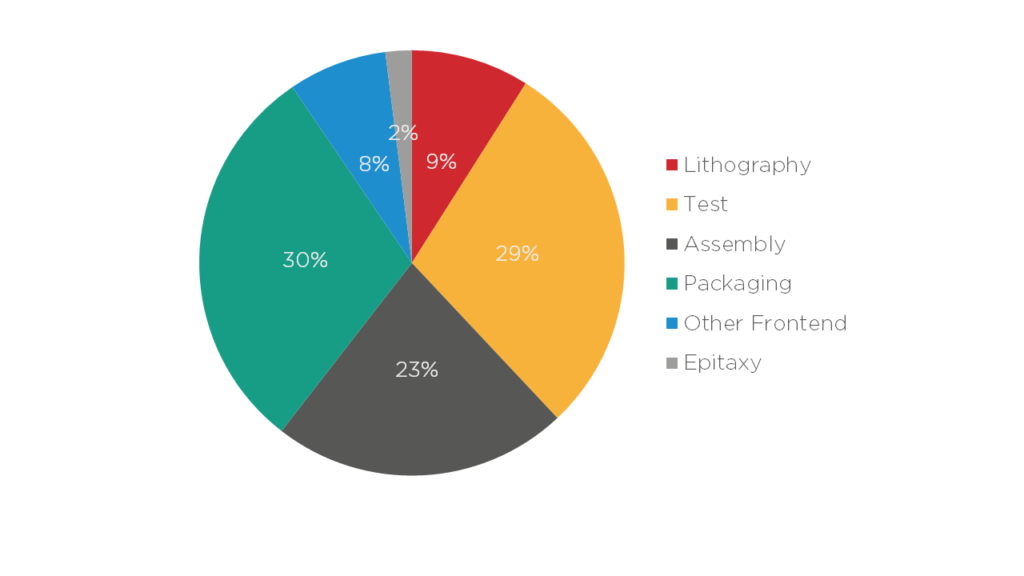
Chip fabrication is a process with many sources of variability, and therefore much testing is required to make sure that the fabricated chip agrees with what was originally designed and simulated. Once that is certified and qualified, the process of packaging and assembling a device with the PIC follows.
While packaging, assembly, and testing are only a small part of the cost of electronic systems, the reverse happens with photonic systems. Researchers at the Technical University of Eindhoven (TU/e) estimate that for most Indium Phosphide (InP) photonics devices, the cost of packaging, assembly, and testing can reach around 80% of the total module cost. There are many research efforts in motion to reduce these costs, which you can learn more about in one of our previous articles.
Especially after the first fabrication run of a new chip, there will be a few rounds of characterization, validation and revisions to make sure the chip performs up to spec. After this first round of characterization and validation, the chip must be made ready for mass production, which requires a series of reliability tests in several environmental different conditions. You can learn more about this process in our previous article on industrial hardening. For example, different applications need different certification of the temperatures in which the chip must operate in.
| Temperature Standard | Temperature Range (°C) | |
| Min | Max | |
| Commercial (C-temp) | 0 | 70 |
| Extended (E-temp) | -20 | 85 |
| Industrial (I-temp) | -40 | 85 |
| Automotive / Full Military | -40 | 125 |
The process of making photonic integrated circuits is incredibly long and complex, and the steps we described in this article are a mere simplification of the entire process. It requires tremendous amount of knowledge in chip design, fabrication, and testing from experts in different fields all around the world. EFFECT Photonics was founded by people who fabricated these chips themselves, understand the process intimately, and developed the connections and network to develop cutting-edge PICs at scale.
Tags: building blocks, c-temp, coherent, die testing, DSP, electron beam lithography, faults, I-temp, imprint lithography, InP, interfaces, optical lithography, reach, scale, wafer testing
The tunable laser is a core component of every optical communication system, both direct detect…
The tunable laser is a core component of every optical communication system, both direct detect and coherent. The laser generates the optical signal modulated and sent over the optical fiber. Thus, the purity and strength of this signal will have a massive impact on the bandwidth and reach of the communication system.
Depending on the material platform, system architecture, and requirements, optical system developers must balance laser parameters—tunability, purity, size, environmental resistance, and power—for the best system performance.
In this article, we will talk about one specific kind of laser—the integrable tunable laser assembly (ITLA)—and when it is needed.
The promise of silicon photonics (SiP) is compatibility with existing electronic manufacturing ecosystems and infrastructure. Integrating silicon components on a single chip with electronics manufacturing processes can dramatically reduce the footprint and the cost of optical systems and open avenues for closer integration with silicon electronics on the same chip. However, the one thing silicon photonics misses is the laser component.
Silicon is not a material that can naturally emit laser light from electrical signals. Decades of research have created silicon-based lasers with more unconventional nonlinear optical techniques. Still, they cannot match the power, efficiency, tunability, and cost-at-scale of lasers made from indium phosphide (InP) and other III-V compound semiconductors.
Therefore, making a suitable laser for silicon photonics does not mean making an on-chip laser from silicon but an external laser from III-V materials such as InP. This light source will be coupled via optical fiber to the silicon components on the chip while maintaining a low enough footprint and cost for high-volume integration. The external laser typically comes in the form of an integrable tunable laser assembly (ITLA).
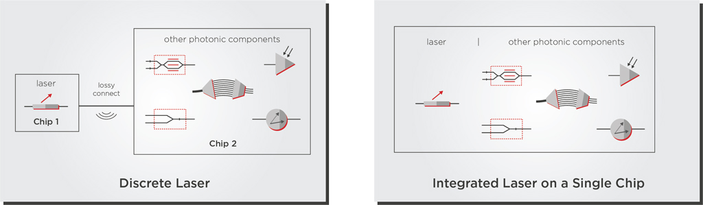
Meanwhile, a photonic chip developer that uses the InP platform for its entire chip instead of silicon can use an integrated laser directly on its chip. Using an external or integrated depends on the transceiver developer’s device requirements, supply chain, and manufacturing facilities and processes. You can read more about the differences in this article.
In summary, an integrable tunable laser assembly (ITLA) is a small external laser that can be coupled to an optical system (like a transceiver) via optical fiber. This ITLA must maintain a low enough footprint and cost for high-volume integration with the optical system.
Since the telecom and datacom industries want to pack more and more transceivers on a single router faceplate, ITLAs need to maintain performance while moving to smaller footprints and lower power consumption and cost.
Fortunately, such ambitious specifications became possible thanks to improved photonic integration technology. The original 2011 ITLA standard from the Optical Internetworking Forum (OIF) was 74mm long by 30.5mm wide. By 2015, most tunable lasers shipped in a micro-ITLA form factor that cut the original ITLA footprint in half. In 2021, the nano-ITLA form factor designed for QSFP-DD and OSFP modules had once again cut the micro-ITLA footprint almost in half. The QSFP-DD modules that house the full transceiver are smaller (78mm by 20mm) than the original ITLA form factor. Stunningly, tunable laser manufacturers achieved this size reduction without impacting laser purity and power.
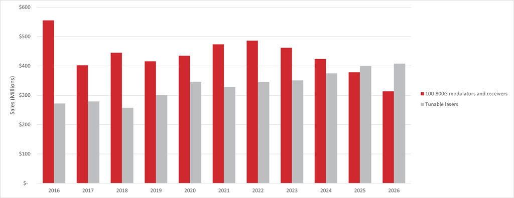
With the increasing demand for coherent transceivers, many companies have performed acquisitions and mergers that allow them to develop transceiver components internally and thus secure their supply. LightCounting predicts that this consolidation will decrease the sales of modulator and receiver components but that the demand for tunable lasers (mainly in the form of ITLAs) will continue to grow. The forecast expects the tunable laser market for transceivers to reach a size of $400M in 2026. We talk more about these market forces in one of our previous articles.
However, the industry consolidation will make it harder for component and equipment manufacturers to source lasers from independent vendors for their transceivers. The market needs more independent vendors to provide high-performance ITLA components that adapt to different datacom or telecom provider needs. Following these trends, at EFFECT Photonics we are not only developing the capabilities to provide a complete, fully-integrated coherent transceiver solution but also the ITLA units needed by vendors who use external lasers.
The world is moving towards tunability. As telecom and datacom industries seek to expand their network capacity without increasing their fiber infrastructure, the sales of tunable transceivers will explode in the coming years. These transceivers need tunable lasers with smaller sizes and lower power consumption than ever.
Some transceivers will use lasers integrated directly on the same chip as the optical engine. Others will have an external laser coupled via fiber to the optical engine. The need for these external lasers led to the development of the ITLA form factors, which get smaller and smaller with every generation.
Tags: coherent, Density, discrete, DSP, full integration, high-performance, independent, InP, ITLA, micro ITLA, nano ITLA, power consumption, reach, SiP, size, tunable, tunable lasers, versatile
Coherent transmission has become a fundamental component of optical networks to address situations where direct…
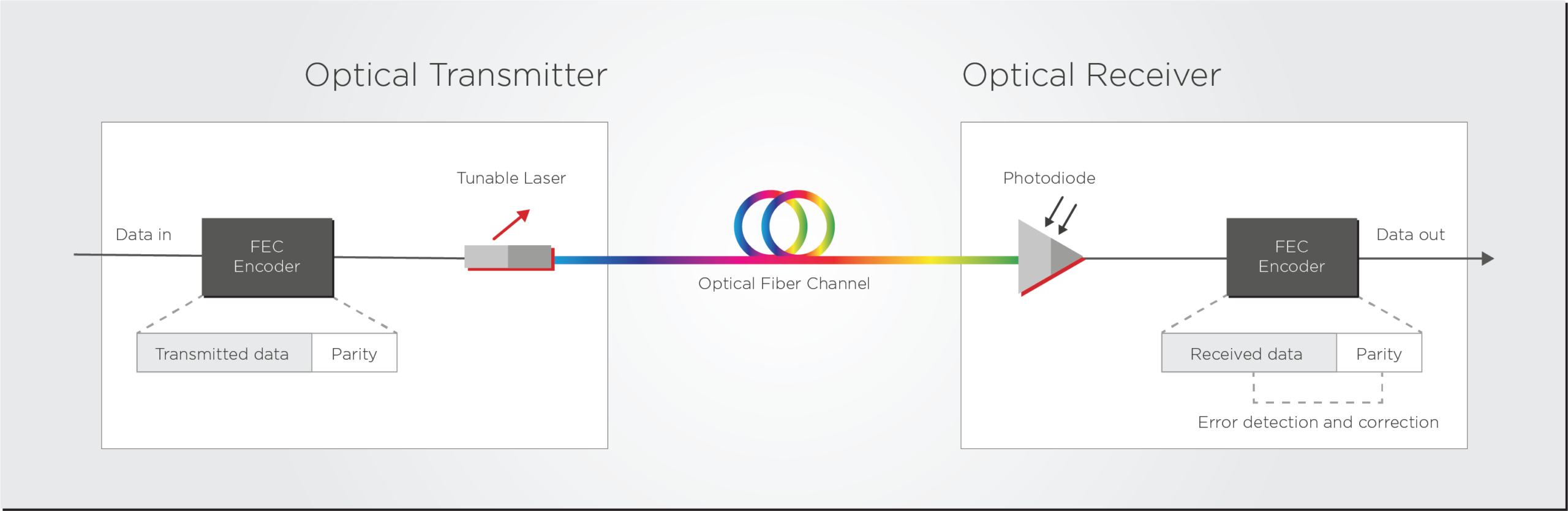
Coherent transmission has become a fundamental component of optical networks to address situations where direct detect technology cannot provide the required capacity and reach.
While Direct Detect transmission only uses the amplitude of the light signal, Coherent optical transmission manipulates three different light properties: amplitude, phase, and polarization. These additional degrees of modulation allow for faster optical signals without compromising the transmission distance. Furthermore, coherent technology enables capacity upgrades without replacing the expensive physical fiber infrastructure on the ground.
However, the demand for data never ceases, and with it, developers of digital signal processors (DSPs) have had to figure out ways to improve the efficiency of coherent transmission. In this article, we will briefly describe the impact of two algorithms that DSP developers use to make coherent transmission more efficient: Forward Error Correction (FEC) and Probabilistic Constellation Shaping (PCS).
Forward Error Correction (FEC) implemented by DSPs has become a vital component of coherent communication systems. FEC makes the coherent link much more tolerant to noise than a direct detect system and enables much longer reach and higher capacity. Thanks to FEC, coherent links can handle bit error rates that are literally a million times higher than a typical direct detect link.
Let’s provide a high-level overview of how FEC works. An FEC encoder adds a series of redundant bits (called overhead) to the transmitted data stream. The receiver can use this overhead to check for errors without asking the transmitter to resend the data.
In other words, FEC algorithms allow the DSP to enhance the link performance without changing the hardware. This enhancement is analogous to imaging cameras: image processing algorithms allow the lenses inside your phone camera to produce a higher-quality image.
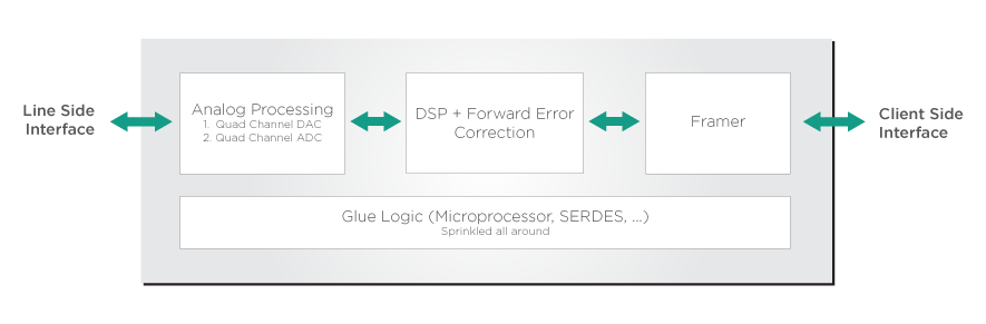
We must highlight that FEC is a block of an electronic DSP engine with its own specialized circuitry and algorithms, so it is a separate piece of intellectual property. Therefore, developing the entire DSP electronic engine (see Figure 2 for the critical component blocks of a DSP) requires ownership or access to specific FEC intellectual property.
DSP developers can transmit more data by transmitting more states in their quadrature-amplitude modulation process. The simplest kind of QAM (4-QAM) uses four different states (usually called constellation points), combining two different intensity levels and two different phases of light.
By using more intensity levels and phases, more bits can be transmitted in one go. State-of-the-art commercially available 400ZR transceivers typically use 16-QAM, with sixteen different constellation points that arise from combining four different intensity levels and four phases. However, this increased transmission capacity comes at a price: a signal with more modulation orders is more susceptible to noise and distortions. That’s why these transceivers can transmit 400Gbps over 100km but not over 1000km.
One of the most remarkable recent advances in DSPs to increase the reach of light signals is Probabilistic Constellation Shaping (PCS). In the typical 16-QAM modulation used in coherent transceivers, each constellation point has the same probability of being used. This is inefficient since the outer constellation points that require more power have the same probability as the inner constellation points that require lower power.
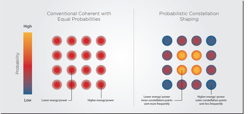
PCS uses the low-power inner constellation points more frequently and the outer constellation points less frequently, as shown in Figure 3. This feature provides many benefits, including improved tolerance to distortions and easier system optimization to specific bit transmission requirements. If you want to know more about it, please read the explainers here and here.
Algorithms like FEC and PCS have usually been proprietary technologies. Equipment and component manufacturers closely guarded their algorithms because they provided a critical competitive advantage. However, this often meant that coherent transceivers from different vendors could not operate with each other, and a single vendor had to be used for the entire network deployment.
Over time, coherent transceivers have increasingly needed to become interoperable, leading to some standardization in these algorithms. For example, the 400ZR standard for data center interconnects uses a public algorithm called concatenated FEC (CFEC). In contrast, some 400ZR+ MSA standards use open FEC (oFEC), which provides a more extended reach at the cost of a bit more bandwidth and energy consumption. For the longest possible link lengths (500+ kilometers), proprietary FECs become necessary for 400G transmission. Still, at least the public FEC standards have achieved interoperability for a large segment of the 400G transceiver market. Perhaps in the future, this could happen with PCS methods.
Future DSPs could switch among different algorithms and methods to adapt to network performance and use cases. For example, let’s look at the case of upgrading a long metro link of 650km running at 100 Gbps with open FEC. The operator needs to increase that link capacity to 400 Gbps, but open FEC could struggle to provide the necessary link performance. However, if the DSP can be reconfigured to use a proprietary FEC standard, the transceiver will be able to handle this upgraded link. Similarly, longer reach could be achieved if the DSP activates its PCS feature.
| 400 ZR | Open ZR+ | Proprietary Long Haul | |
| Target Application | Edge data center interconnect | Metro, Regional data center interconnect | Long-Haul Carrier |
| Target Reach @ 400G | 120km | 500km | 1000 km |
| Form Factor | QSFP-DD/OSFP | QSFP-DD/OSFP | QSFP-DD/OSFP |
| FEC | CFEC | oFEC | Proprietary |
| Standards / MSA | OIF | OpenZR+ MSA | Proprietary |
The entire field of communication technology can arguably be summarized with a single question: how can we transmit more information into a single frequency-limited signal over the longest possible distance?
DSP developers have many tools to answer this question, and two of them are FEC and PCS. Both technologies make coherent links much more tolerant of noise and can extend their reach. Future pluggables that handle different use cases must use different coding, error coding, and modulation schemes to adapt to different network requirements.
There are still many challenges ahead to improve DSPs and make them transmit even more bits in more energy-efficient ways. Now that EFFECT Photonics has incorporated talent and intellectual property from Viasat’s Coherent DSP team, we hope to contribute to this ongoing research and development and make transceivers faster and more sustainable than ever.
Tags: coherent, constellation shaping, DSP, DSPs, error compensation, FEC, PCS, power, Proprietary, reach, reconfigurable, standardized, standards
Smaller data centers placed locally have the potential to minimize latency, overcome inconsistent connections, and…
Smaller data centers placed locally have the potential to minimize latency, overcome inconsistent connections, and store and compute data closer to the end user. These benefits are causing the global market for edge data centers to explode, with PWC predicting that it will nearly triple from $4 billion in 2017 to $13.5 billion in 2024.
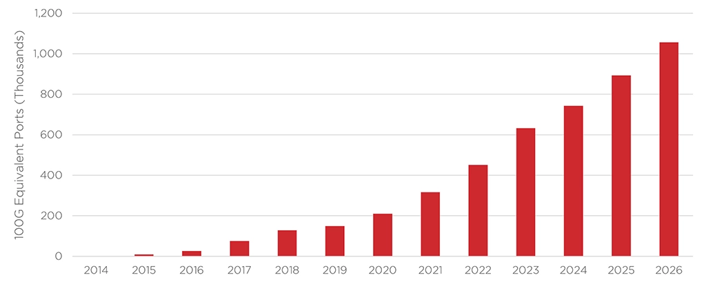
As edge data centers become more common, the issue of interconnecting them becomes more prominent. This situation motivated the Optical Internetworking Forum (OIF) to create the 400ZR and ZR+ standards for pluggable modules. With small enough modules to pack a router faceplate densely, the datacom sector could profit from a 400ZR solution for high-capacity data center interconnects of up to 80km. Cignal AI forecasts that 400ZR shipments will dominate the edge applications, as shown in the figure below.
The 400ZR standard has made coherent technology and dense wavelength division multiplexing (DWDM) the dominant solution in the metro data center interconnects (DCIs) space. Datacom provider operations teams found the simplicity of coherent pluggables very attractive. There was no need to install and maintain additional amplifiers and compensators as in direct detect technology. A single coherent transceiver plugged into a router could fulfill the requirements.
However, there are still obstacles that prevent coherent from becoming dominant in shorter-reach DCI links at the campus (< 10km distance) and intra-datacenter (< 2km distance) level. These spaces require more optical links and transceivers, and coherent technology is still considered too power-hungry and expensive to become the de-facto solution here.
Fortunately, there are avenues for coherent technology to overcome these barriers. By embracing multi-laser arrays, DSP co-design, and electronic ecosystems, coherent technology can mature and become a viable solution for every data center interconnect scenario.
Earlier this year, Intel Labs demonstrated an eight-wavelength laser array fully integrated on a silicon wafer. These milestones are essential for optical transceivers because the laser arrays can allow for multi-channel transceivers that are more cost-effective when scaling up to higher speeds.
Let’s say we need an intra-DCI link with 1.6 Terabits/s of capacity. There are three ways we could implement it:
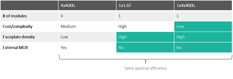
Multi-laser array and multi-channel solutions will become increasingly necessary to increase link capacity in coherent systems. They will not need more slots in the router faceplate while simultaneously avoiding the higher cost and complexity of increasing the speed with just a single channel.
Transceiver developers often source their DSP, laser, and optical engine from different suppliers, so all these chips are designed separately from each other. This setup reduces the time to market and simplifies the research and design processes but comes with trade-offs in performance and power consumption.
In such cases, the DSP is like a Swiss army knife: a jack of all trades designed for different kinds of optical engines but a master of none. For example, current DSPs are designed to be agnostic to the material platform of the photonic integrated circuit (PIC) they are connected to, which can be Indium Phosphide (InP) or Silicon. Thus, they do not exploit the intrinsic advantages of these material platforms. Co-designing the DSP chip alongside the PIC can lead to a much better fit between these components.
To illustrate the impact of co-designing PIC and DSP, let’s look at an example. A PIC and a standard platform-agnostic DSP typically operate with signals of differing intensities, so they need some RF analog electronic components to “talk” to each other. This signal power conversion overhead constitutes roughly 2-3 Watts or about 10-15% of transceiver power consumption.
However, the modulator of an InP PIC can run at a lower voltage than a silicon modulator. If this InP PIC and the DSP are designed and optimized together instead of using a standard DSP, the PIC could be designed to run at a voltage compatible with the DSP’s signal output. This way, the optimized DSP could drive the PIC directly without needing the RF analog driver, doing away with most of the power conversion overhead we discussed previously.
Additionally, the optimized DSP could also be programmed to do some additional signal conditioning that minimizes the nonlinear optical effects of the InP material, which can reduce noise and improve performance.
Making coherent optical transceivers more affordable is a matter of volume production. As discussed in a previous article, if PIC production volumes can increase from a few thousand chips per year to a few million, the price per optical chip can decrease from thousands of Euros to mere tens of Euros. Achieving this production goal requires photonics manufacturing chains to learn from electronics and leverage existing electronics manufacturing processes and ecosystems.
While vertically-integrated PIC development has its strengths, a fabless model in which developers outsource their PIC manufacturing to a large-scale foundry is the simplest way to scale to production volumes of millions of units. Fabless PIC developers can remain flexible and lean, relying on trusted large-scale manufacturing partners to guarantee a secure and high-volume supply of chips. Furthermore, the fabless model allows photonics developers to concentrate their R&D resources on their end market and designs instead of costly fabrication facilities.
Further progress must also be made in the packaging, assembly, and testing of photonic chips. While these processes are only a small part of the cost of electronic systems, the reverse happens with photonics. To become more accessible and affordable, the photonics manufacturing chain must become more automated and standardized. It must move towards proven and scalable packaging methods that are common in the electronics industry.
If you want to know more about how photonics developers can leverage electronic ecosystems and methods, we recommend you read our in-depth piece on the subject.
Coherent transceivers are already established as the solution for metro Data Center Interconnects (DCIs), but they need to become more affordable and less power-hungry to fit the intra- and campus DCI application cases. Fortunately, there are several avenues for coherent technology to overcome these cost and power consumption barriers.
Multi-laser arrays can avoid the higher cost and complexity of increasing capacity with just a single transceiver channel. Co-designing the optics and electronics can allow the electronic DSP to exploit the intrinsic advantages of specific photonics platforms such as indium phosphide. Finally, leveraging electronic ecosystems and processes is vital to increase the production volumes of coherent transceivers and make them more affordable.
By embracing these pathways to progress, coherent technology can mature and become a viable solution for every data center interconnect scenario.
Tags: campus, cloud, cloud edge, codesign, coherent, DCI, DSP, DSPs, DWDM, integration, intra, light sources, metro, modulator, multi laser arrays, photonic integration, PIC, power consumption, wafer testing© 2025 EFFECT PHOTONICS All rights reserved. T&C of Website - T&C of Purchase - Privacy Policy - Cookie Policy - Supplier Code of Conduct