Last year, EFFECT Photonics taped out the world’s first fully integrated coherent optical transceiver chip.…
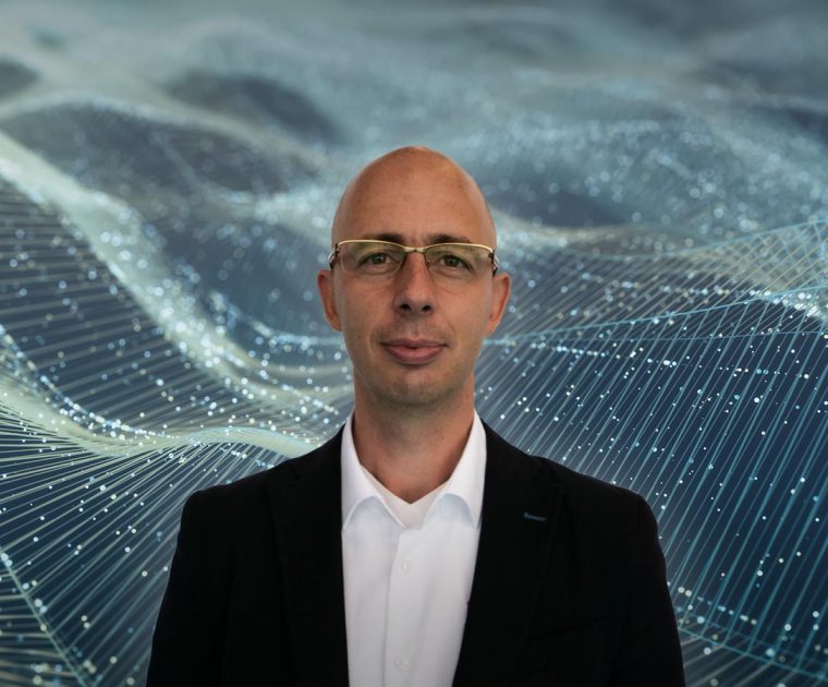
Last year, EFFECT Photonics taped out the world’s first fully integrated coherent optical transceiver chip. We are now ready to turn this engineering breakthrough into a product. To lead this process, EFFECT Photonics has hired Vladimir Veljanovski as our first Coherent Product Line Manager. To give you more insight into our new colleague and what drives him, we asked him a few questions.
Tell us a little more about yourself and your background
I was born in Macedonia and moved to Germany for my university studies, graduating in 2006 with an Engineering degree in Communication and Information Technology from the Technical University in Munich. I did my master thesis with the R&D department of Siemens Fixed Networks (later Coriant) and started working there after graduation. I started my job by simulating optical transmission systems and extracting system design rules. Soon after, I moved to the lab, which definitely attracted me more as it was closer to reality and work done on the field.
Around that time, we started testing our first 40G coherent product in the lab. Coherent was a major technology change, and customers were struggling to believe and buy into it. Hence, R&D needed to go to the customers and demonstrate the new technology. That’s when I discovered my preference for working closer to the customers. I remained in this customer-facing role until 2014, doing lots of introductory work for coherent technology in terrestrial and submarine networks. In 2014, I moved to Switzerland to work for Huawei in a technical sales role as the Sales Project Manager responsible for the Swisscom transport network. In four exciting years there, we renewed the network by introducing 200G and 400G coherent products into the network backbone and 100G coherent into the metro network.
After the Huawei experience, I wanted more of a network-level overview, which was hard to get when working with the network of a telecom carrier. Thus, I spent the next two years working in the enterprise environment. The company was smaller and more easily manageable. There I could see the whole network as an entity, not just the optics but also the switching, the firewalls, the network management, etc. And in June 2021, I joined EFFECT Photonics. I am thrilled with this transition, even though we have a lot of work to bring the product out as soon as possible.
What do you find exciting about coherent technology?
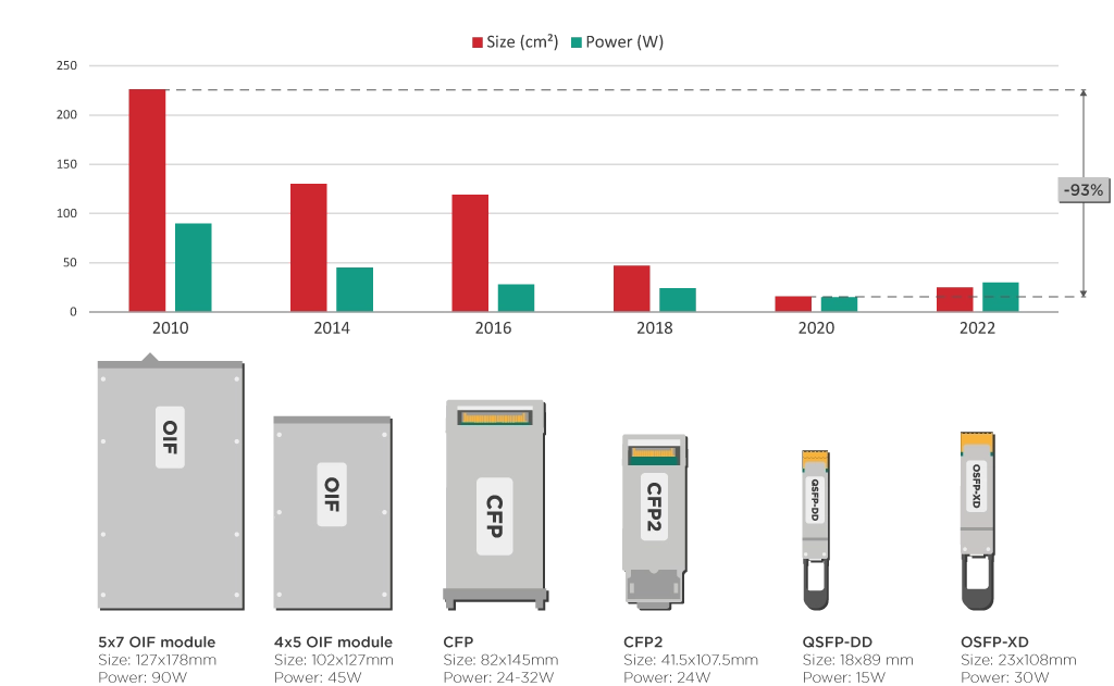
Coherent technology is not new. It has been around for a while. However, it is incredible that now those complicated benchtop systems I built in the lab back in 2009, with all the discrete components that were cumbersome to connect, can now fit into something the size of a sugar cube thanks to photonic integration. And these systems even have better performance than back then. You see that progress and think, “man, that’s awesome!”.
Coherent technology was reserved for premium long-distance links where performance is everything. Metro and access networks could not use this higher-performance technology since on the one hand, it was too bulky and expensive, and on the other, the bandwidth demand was yet to grow.
Photonic integration technology like EFFECT’ Photonics’ helped bring these big, proprietary, and expensive systems into a router pluggable form factor. This tech has squeezed more performance into a smaller area and at lower power consumption, making the device more cost-effective. Photonic integration will be a disruptive technology that will simplify network design and operation and reduce the capital and operating expenses of network operators.
What do you find exciting about working at EFFECT Photonics?
I love working with smart people with a good team spirit. I get to study and learn new things, and I continue to grow and challenge myself, which makes all the work even more fun.
I figured out that by working at EFFECT Photonics, I would be surrounded by great professionals who have worked on photonic integration for ten years or more and know and identify with this technology very well. It’s a fascinating and challenging environment for me to be in.
On that note, photonic integration technology was a big reason why I chose to work at EFFECT Photonics. I was amazed to see how a company of this size, with relatively few people, can work on such a potentially disruptive technology. I get to work on new and exciting technology, and at the same time, I can get to know almost everyone in the company. I clearly feel the “scale-up winds” blowing in my daily work.
Having worked in both R&D and sales of coherent products with network carriers and enterprise providers, Vladi possesses deep insight into coherent technology itself and how to sell it to customers. At EFFECT Photonics, we are excited to work with him, and we look forward to what he can do to turn our technology into a fantastic coherent product.
Tags: coherent, Integrated Photonics, photonic integration