– SemiconductorToday

⚠️ Website Under Construction

– SemiconductorToday

– LightWave

– The PIC features support for 100G, 400G and 800G ZR applications and will become…
– The PIC features support for 100G, 400G and 800G ZR applications and will become the cornerstone of the smallest tunable laser assembly for coherent applications.
EFFECT Photonics, a leading developer of highly integrated optical solutions, announced today the verification of its fully integrated tunable laser InP-based Photonic Integrated Circuit (PIC), the core enabler powering its digital Pico Integrated Tunable Laser Assembly (pITLA). Tunable lasers are a core component of coherent optical systems enabling Dense Wavelength Division Multiplexing (DWDM), which allows network operators to expand their network capacity without expanding the existing fiber infrastructure. With this milestone, the tunable laser InP-based Photonic Integrated Circuit (PIC) has successfully passed a series of tests showing required performance items outlined by IEEE Std. 802.3-2022, 100GBASE-ZR.
Unlike tunable laser assemblies currently available, the core of EFFECT Photonics digital pITLA is a tunable laser implemented fully as a monolithic integrated InP PIC. This enables advantages such as the ability to achieve a compact footprint, higher assembly yields, and ease of integration into pluggable form factors. The InP PIC is the only solution to integrate the gain section, laser cavity, optical amplifier, and wavelength locker into one chip. By incorporating these functions on a single chip and including the control functions in the assembly, the user can easily communicate and control the laser by simply providing digital commands.
“In the last decade, the industry has made impressive strides in reducing the size of crucial coherent optical functions, making way for digital coherent modules. EFFECT Photonics pITLA sets a new precedent in photonic integration by eliminating the need for external micro-optics for control of tunable lasers,” said Roberto Marcoccia, CEO of EFFECT Photonics. “Our monolithic approach maintains all vital functions while drastically reducing the device’s overall size to a smaller form factor previously unattainable.”
Purposely designed to simplify the design of small form factor pluggables, the integrated InP PIC is the foundation of EFFECT Photonics new pITLA, providing an outstanding blend of power, cost-effectiveness, and compactness. It paves the way for the effortless and cost-efficient design of coherent pluggables, opening up new possibilities for the industry.
To learn more about the EFFECT Photonics pITLA, visit Stand 547 at ECOC23 or attend EFFECT Photonics’ Market Focus Session “Power and Integration: InP for Coherent Transceivers at the Network Edge” on Monday, October 2 at 12pm.
Roberto Marcoccia, CEO of EFFECT PhotonicsIn the last decade, the industry has made impressive strides in reducing the size of crucial coherent optical functions, making way for digital coherent modules. EFFECT Photonics pITLA sets a new precedent in photonic integration by eliminating the need for external micro-optics for control of tunable lasers. Our monolithic approach maintains all vital functions while drastically reducing the device’s overall size to a smaller form factor previously unattainable.
Purposely designed to simplify the design of small form factor pluggables, the integrated InP PIC is the foundation of EFFECT Photonics new pITLA, providing an outstanding blend of power, cost-effectiveness, and compactness. It paves the way for the effortless and cost-efficient design of coherent pluggables, opening up new possibilities for the industry.
To learn more about the EFFECT Photonics pITLA, visit Stand 547 at ECOC23 or attend EFFECT Photonics’ Market Focus Session “Power and Integration: InP for Coherent Transceivers at the Network Edge” on Monday, October 2 at 12pm.
Where Light Meets Digital – EFFECT Photonics is a highly vertically integrated, independent optical systems company addressing the need for high-performance, affordable optic solutions driven by the ever-increasing demand for bandwidth and faster data transfer capabilities. Using our company’s field-proven digital signal processing and forward error correction technology and ultra-pure light sources, we offer compact form factors with seamless integration, cost efficiency, low power, and security of supply. By leveraging established microelectronics ecosystems, we aim to make our products affordable and available in high volumes to address the challenges in 5G and beyond, access-ready coherent solutions, and cloud and cloud edge services. For more information, please visit: www.effectphotonics.com. Follow EFFECT Photonics on LinkedIn and Twitter.
# # #
Media Contact:
Colleen Cronin
EFFECT Photonics
colleencronin@effectphotonics.com

EFFECT Photonics’ coherent technology portfolio has grown in the last two years, including coherent transceivers,…
EFFECT Photonics’ coherent technology portfolio has grown in the last two years, including coherent transceivers, laser sources, and digital signal processors. To lead this portfolio, EFFECT Photonics has hired Charlie Fu as our new Coherent Product Manager. To give you more insight into our new colleague and what drives him, we asked him a few questions.

So, my whole life is actually devoted to photonics. When I was a student in college, I studied optoelectronics, and my undergraduate project was doing a diode laser response curve. I also worked hard in graduate school with my supervisor in the lab to test coherent lasers back in the early 1990s when this technology was in its early stages. Back then, the laser was based on bulk micro-optics and could transmit for maybe 10 kilometers of distance. It was a significantly bigger package than now.
I was very lucky to start my career during an optical communications boom, working on fiber optic devices and modules with JDS Uniphase. I built my career there, starting with optical design and a lot of learning.
I then moved to a network company, Nortel Networks, designing links for long-haul transmission systems. We ensured the performance of the optical system and how to specify all the optical components modules to ensure the required performance. Nortel had a very ambitious project at the time. It was a technology challenge of transmitting 40G long haul transmission. Perhaps too ambitious, the year 2000 was perhaps too early still to go coherent.
So yeah, my whole career has been devoted to optics. From working as a hardware design engineer and learning all the optical transponder optical module design. Working with a few well-known brands such as Oclaro.
So I think EFFECT Photonics has a good combination of people and technology, with many interesting technology innovations. The entrepreneurial drive to achieve success.
What attracted me the most was the core technology message of where light meets digital. If we look around, quite a lot of companies have photonics technology OR digital signal processing (DSP) technology. But almost no one has both IP for DSP and photonic technology. Having those IPs puts EFFECT Photonics in a very unique, prestigious position.
I still believe coherent technology is in its infant stage in its application to optical communication. There are still a lot of things to do. For example, moving it to access network communications instead of just long haul. That’s something EFFECT Photonics wants to do and why I’m very excited about the future of our coherent optics.
The coherent system implementation may have changed a lot and gotten smaller, but the technology, the core concept, it’s still exactly the same as 30 years ago. I want to help develop these new systems with the new technology available to optics in the semiconductor sector.
I’m very excited to develop products that use these new technologies, hence why I am now in a Product Manager position.
I’m very excited to leverage my experience and knowledge and I’m very confident I can make a positive contribution to EFFECT Photonics in product design and development.
Tags: Access Network Communication, Charlie Fu, coherent, Coherent Product Manager, Core Technology Message, digital signal processing (DSP), EFFECT Photonics, Entrepreneurial Drive, Fiber Optic Devices, Innovative Technology, Integrated Photonics, IP for DSP and Photonic Technology, Long-Haul Transmission, Optical Communication, Optical Design, Optical Module Design, Optical Transponder, Photonic Technology, Photonics, Photonics Technology, Product Design, Product Development, Semiconductor Sector
Join EFFECT Photonics from October 2nd-4th, 2023 at ECOC Exhibition in Sec, Glasgow, Scotland. ECOC is the largest optical communications exhibition in Europe and a key meeting place for decision-makers. Come and discover firsthand how our technology is transforming where light meets digital, visit booth #547 to learn how EFFECT Photonics’ full portfolio of optical building blocks are enabling 100G coherent to the network edge and next-generation applications.
Build Your Own 100G ZR Coherent Module
At this year’s ECOC, see how easy and affordable it can be to upgrade existing 10G links to a more scalable 100G coherent solution! Try your hand at constructing a 100G ZR coherent module specifically designed for the network edge utilizing various optical building blocks including tunable lasers, DSPs and optical subassemblies.
Tune Your Own PIC (Photonic Integrated Circuit)
Be sure to stop by stand #547 to tune your own PIC with EFFECT Photonics technology. In this interactive and dynamic demonstration, participants can explore first-hand the power of EFFECT Photonics solutions utilizing various parameters and product configurations.
Our experts are also available to discuss customer needs and how EFFECT Photonics might be able to assist. To schedule a meeting, please email marketing@effectphotonics.com
Tags: 100 ZR, 100G, 100gcoherent, access, access networks, bringing100Gtoedge, cloud, cloudedge, coherent, coherentoptics, datacenters, DSP, DSPs, ECOC, ECOC2023, EFFECT Photonics, Integrated Photonics, networkedge, opticcommunications, Optics, photonic integration, Photonics, PIC, tunablelasers, wherelightmeetsdigital
In today’s rapidly evolving world, traditional technologies such as microelectronics are increasingly struggling to match…
In today’s rapidly evolving world, traditional technologies such as microelectronics are increasingly struggling to match the rising demands of sectors such as communication, healthcare, energy, and manufacturing. These struggles can result in slower data transmission, more invasive diagnostics, or excessive energy consumption. Amidst these challenges, there is a ray of hope: photonics.
Photonics is the study and application of light generation, manipulation, and detection, often aiming to transmit, control, and sense light signals. Its goals and even the name “photonics” are born from its analogy with electronics: photonics aims to transmit, control, and sense photons (the particles of light) in similar ways to how electronics do with electrons (the particles of electricity).
Photons can travel more quickly and efficiently than electrons, especially over long distances. Photonic devices can be manufactured on a semiconductor process similar to the one used by microelectronics, so they have the potential to be manufactured in small packages at high volumes. Due to these properties, photonics can drive change across multiple industries and technologies by enabling faster and more sustainable solutions manufactured at scale.
Two of the biggest sectors photonics can impact are communications and sensing.
Light is the fastest information carrier in the universe and can transmit this information while dissipating less heat and energy than electrical signals. Thus, photonics can dramatically increase communication networks’ speed, reach, and flexibility and cope with the ever-growing demand for more data. And it will do so at a lower energy cost, decreasing the Internet’s carbon footprint.
The webpage you are reading was originally a stream of 0 and 1s that traveled through an optical fiber to reach you. Fiber networks need some optical transceiver that transmits and receives the light signal through the fiber. These transceivers were initially bulky and inefficient, but advances in integrated photonics and electronics have miniaturized these transceivers into the size of a large USB stick.
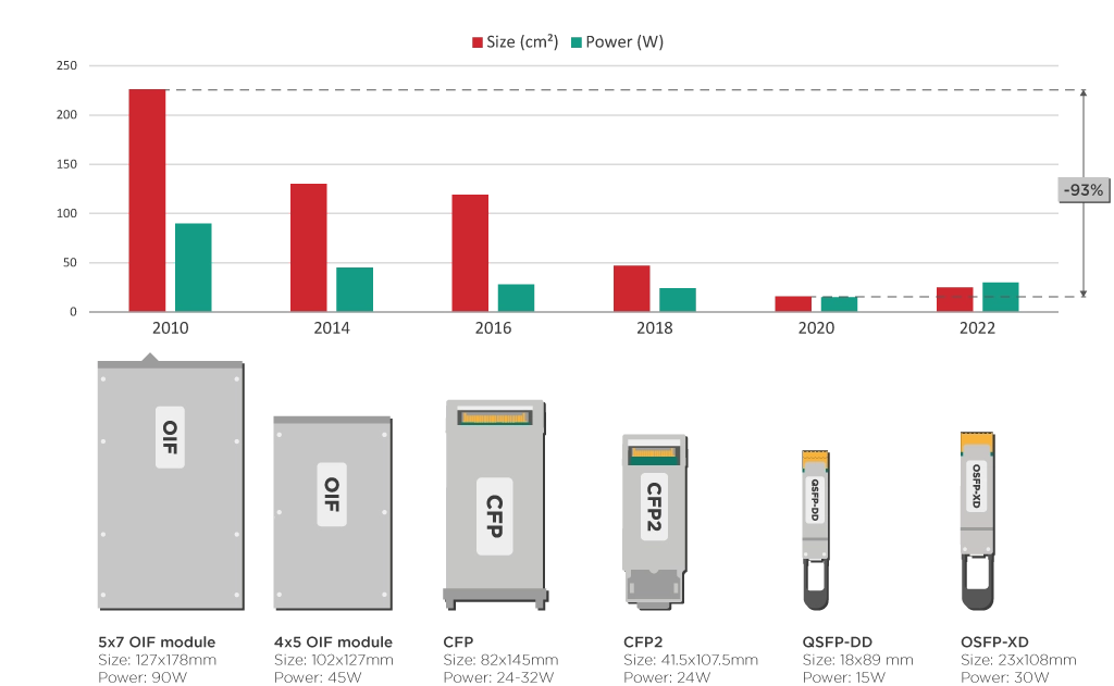
Aside from fiber communications, photonics can also deliver solutions beyond traditional radio communications. For example, optical transmission over the air or space could handle links between different mobile network sites, cars, or satellites.
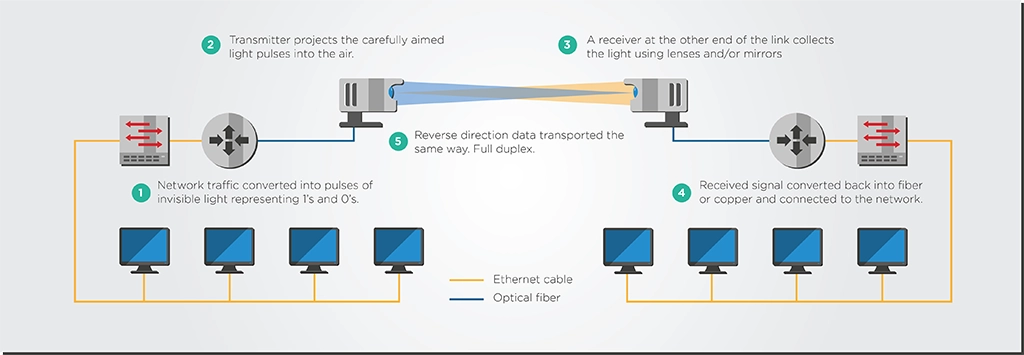
There are multiple sensing application markets but their core technology is the same. They need a small device that sends out a known pulse of light, accurately detects how the light comes back, and calculates the properties of the environment from that information. It’s a simple but quite powerful concept.
This concept is already being used to implement LIDAR systems that help self-driving cars determine the location and distance of people and objects. However, there is also potential to use this concept in medical and agrifood applications, such as looking for undesired growths in the human eye or knowing how ripe an apple is.
Photonics can make many industries more energy efficient. One of the photonics’ success stories is light-emitting diodes (LEDs) manufactured at scale through semiconductor processes. LED lighting sales have experienced explosive growth in the past decade, quickly replacing traditional incandescent and fluorescent light bulbs that are less energy efficient. The International Energy Agency (IEA) estimates that residential LED sales have risen from around 5% of the market in 2013 to about 50% in 2022.
Greater integration is also vital for energy efficiency. In many electronic and photonic devices, the interconnections between different components are often sources of losses and inefficiency. A more compact, integrated device will have shorter and more energy-efficient interconnections. For example, Apple’s system-on-chip processors fully integrate all electronic processing functions on a single chip. As shown in the table below, these processors are significantly more energy efficient than the previous generations of Apple processors.
| 𝗠𝗮𝗰 𝗠𝗶𝗻𝗶 𝗠𝗼𝗱𝗲𝗹 | 𝗣𝗼𝘄𝗲𝗿 𝗖𝗼𝗻𝘀𝘂𝗺𝗽𝘁𝗶𝗼𝗻 | |
| 𝗜𝗱𝗹𝗲 | 𝗠𝗮𝘅 | |
| 2023, M2 | 7 | 5 |
| 2020, M1 | 7 | 39 |
| 2018, Core i7 | 20 | 122 |
| 2014, Core i5 | 6 | 85 |
| 2010, Core 2 Duo | 10 | 85 |
| 2006, Core Solo or Duo | 23 | 110 |
| 2005, PowerPC G4 | 32 | 85 |
| Table 1: Comparing the power consumption of a Mac Mini with an M1 and M2 SoC chips to previous generations of Mac Minis. [Source: Apple’s website] | ||
The photonics industry can set a similar goal to Apple’s system-on-chip. By integrating all the optical components (lasers, detectors, modulators, etc.) on a single chip can minimize the losses and make devices such as optical transceivers more efficient.
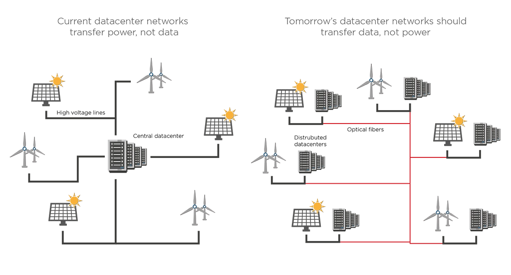
There are other ways for photonics to aid energy efficiency goals. For example, photonics enables a more decentralized system of data centers with branches in different geographical areas connected through high-speed optical fiber links to cope with the strain of data center clusters on power grids. The Dutch government has already proposed this kind of decentralization as part of its spatial strategy for data centers.
Photonics can have an even greater impact on the world if it becomes as readily available and easy to use as electronics.
We need to buy photonics from a catalog as we do with electronics, have datasheets that work consistently, be able to solder it to a board and integrate it easily with the rest of the product design flow.
Tim Koene – Chief Technology Officer, EFFECT Photonics
Today, photonics is still a ways off from achieving this goal. Photonics manufacturing chains are not at a point where they can quickly produce millions of integrated photonic devices per year. While packaging, assembly, and testing are only a small part of the cost of electronic systems, they are 80% of the total module cost in photonics, as shown in the figure below.
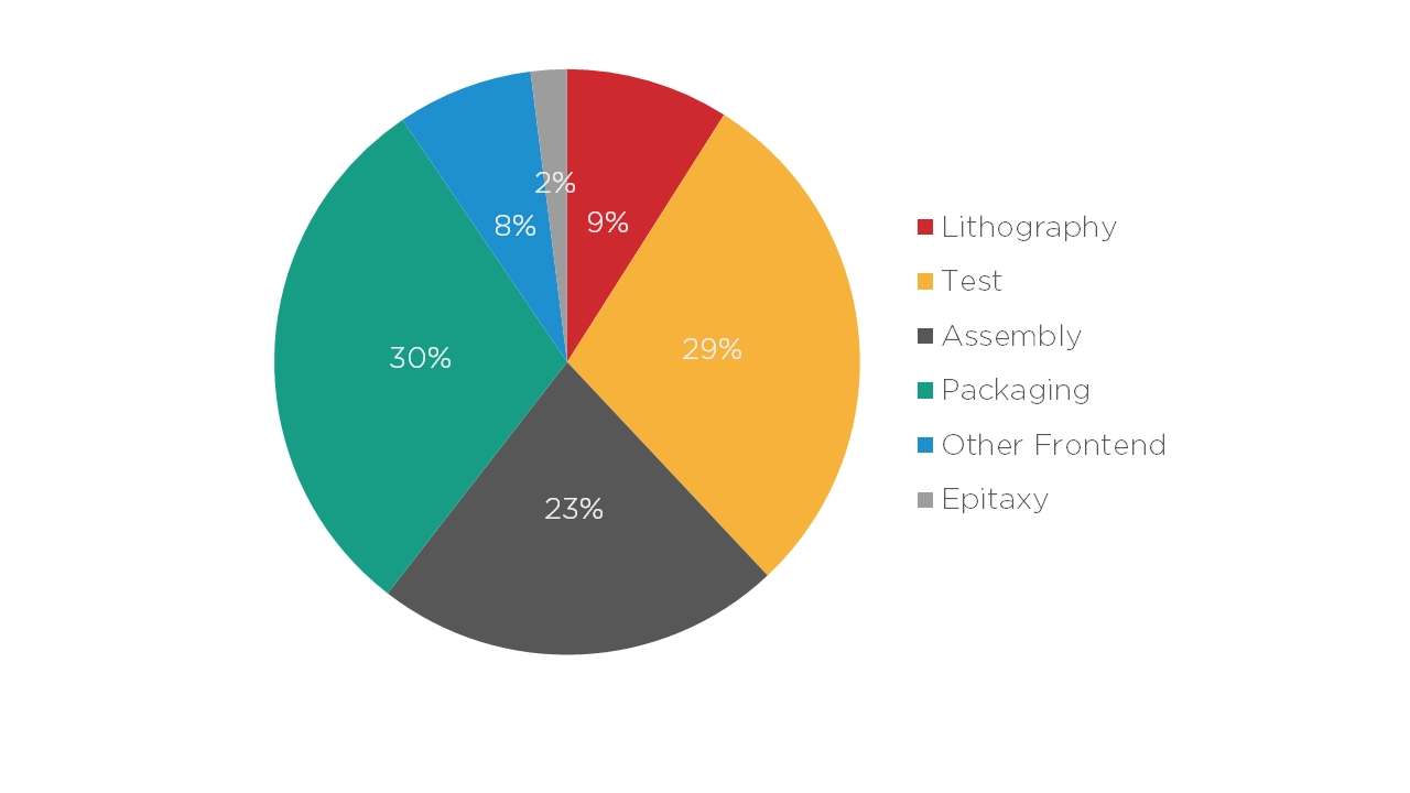
To scale and become more affordable, the photonics manufacturing chains must become more automated and leverage existing electronic packaging, assembly, and testing methods that are already well-known and standardized. Technologies like BGA-style packaging and flip-chip bonding might be novel for photonics developers who started implementing them in the last five or ten years, but electronics embraced these technologies 20 or 30 years ago. Making these techniques more widespread will make a massive difference in photonics’ ability to scale up and become as available as electronics.
The roadmap of scaling integrated photonics and making it more accessible is clear: it must leverage existing electronics manufacturing processes and ecosystems and tap into the same economy-of-scale principles as electronics. Implementing this roadmap, however, requires more investment in photonics. While such high-volume photonics manufacturing demands a higher upfront investment, the resulting high-volume production line will drive down the cost per device and opens them up to a much larger market. That’s the process by which electronics revolutionized the world.
By harnessing the power of light, integrated photonics can offer faster and more sustainable solutions to address the evolving challenges faced by various sectors, including communication, healthcare, energy, and manufacturing. However, for photonics to truly scale and become as accessible as electronics, more investment is necessary to scale production and adapt existing electronics processes to photonics. This scaling will drive down production costs, making integrated photonics more widely available and paving the way for its impactful integration into numerous technologies across the globe.
Tags: Accessibility, Advancements, Biosensors, Challenges, Communication, Cost reduction, Economic growth, Economies of scale, EFFECT Photonics, Evolving demands, Fiber-optic networks, future, Future returns, Healthcare, innovation, Investing in photonics, Investments, LEDs, Light-based technologies, Limitations, Manufacturing, Manufacturing capabilities, Medical imaging, New solutions, Optical diagnostics, Photonic devices, Photonics, Promising industry, Renewable energy technologies, Scalable communication systems, Solar cells, Traditional technologies
– Link Magazine
While packaging, assembly, and testing are only a small part of the cost of electronic…
While packaging, assembly, and testing are only a small part of the cost of electronic systems, the reverse happens with photonic integrated circuits (PICs) and their subassemblies. Researchers at the Technical University of Eindhoven (TU/e) estimate that for most Indium Phosphide (InP) photonics devices, the cost of packaging, assembly, and testing can reach around 80% of the total module cost.

To trigger a revolution in the use of photonics worldwide, it needs to be as easy to manufacture and use as electronics. In the words of EFFECT Photonics’ Chief Technology Officer, Tim Koene: “We need to buy photonics from a catalog as we do with electronics, have datasheets that work consistently, be able to solder it to a board and integrate it easily with the rest of the product design flow.”
This article will explore three key avenues to improve optical subassemblies and packaging for photonic devices.
A key way to improve photonics manufacturing is to learn from electronics packaging, assembly, and testing methods that are already well-known and standardized. After all, building a new special production line is much more expensive than modifying an existing production flow.
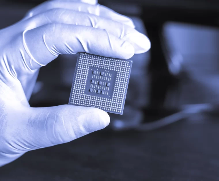
One electronic technique essential to transfer into photonics is ball-grid array (BGA) packaging. BGA-style packaging has grown popular among electronics manufacturers over the last few decades. It places the chip connections under the chip package, allowing more efficient use of space in circuit boards, a smaller package size, and better soldering.
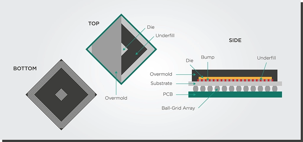
Another critical technique to move into photonics is flip-chip bonding. This process is where solder bumps are deposited on the chip in the final fabrication step. The chip is flipped over and aligned with a circuit board for easier soldering.
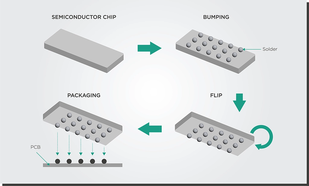
These might be novel technologies for photonics developers who have started implementing them in the last five or ten years. However, the electronics industry embraced these technologies 20 or 30 years ago. Making these techniques more widespread will make a massive difference in photonics’ ability to scale up and become as available as electronics.
Adopting BGA-style packaging and flip-chip bonding techniques will make it easier for PICs to survive this soldering process. There is ongoing research and development worldwide, including at EFFECT Photonics, to transfer more electronics packaging methods into photonics. PICs that can handle being soldered to circuit boards allow the industry to build optical subassemblies that are more accessible to the open market and can go into trains, cars, or airplanes.
Economics of scale is a crucial principle behind electronics manufacturing, and we must apply it to photonics too. The more components we can integrate into a single chip and the more chips we can integrate into a single wafer, the more affordable the photonic device becomes. If production volumes increase from a few thousand chips per year to a few million, the price per optical chip can decrease from thousands of Euros to mere tens of Euros. This must be the goal for the photonics industry in general.
By integrating all optical components on a single chip, we also shift the complexity from the assembly process to the much more efficient and scalable semiconductor wafer process. Assembling and packaging a device by interconnecting multiple photonic chips increases assembly complexity and costs. On the other hand, combining and aligning optical components on a wafer at a high volume is much easier, which drives down the device’s cost.
Deepening photonics integration will also have a significant impact on power consumption. Integrating all the optical components (lasers, detectors, modulators, etc.) on a single chip can minimize the losses and make devices such as optical transceivers more efficient. This approach doesn’t just optimize the efficiency of the devices themselves but also of the resource-hungry chip manufacturing process.
Over the last decade, technological progress in tunable laser packaging and integration has matched the need for smaller footprints. In 2011, tunable lasers followed the multi-source agreement (MSA) for integrable tunable laser assemblies (ITLAs). By 2015, tunable lasers were sold in the more compact Micro-ITLA form factor, which cut the original ITLA package size in half. And in 2019, laser developers (see examples here and here) announced a new Nano-ITLA form factor that reduced the size by almost half again.
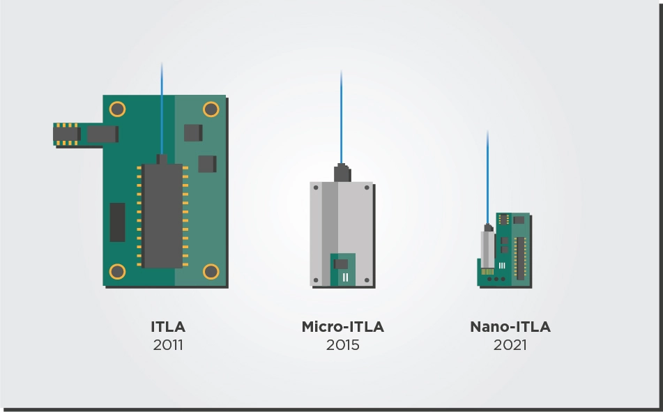
Reducing the footprint of tunable lasers in the future will need even greater integration of their parts. For example, every tunable laser needs a wavelength locker component that can stabilize the laser’s output regardless of environmental conditions such as temperature. Integrating the wavelength locker component on the laser chip instead of attaching it externally would help reduce the laser package’s footprint and power consumption.
Another aspect of optimizing laser module footprint is allowing transceiver developers to mix and match their building blocks. For example, traditional ITLAs in transceivers contain the temperature control driver and power converter functions. However, the main transceiver board can usually provide these functions too. A setup in which the main board performs these driver and converter functions would avoid the need for redundant elements in both the main board and tunable laser.
Finally, the future of laser packaging will also involve packaging more multi-laser arrays. As explained in a previous article, multi-laser arrays will become increasingly necessary to increase link capacity in coherent systems. They will not need more slots in the router faceplate while avoiding the higher cost and complexity of increasing the speed with a single laser channel.
Improving subassemblies and packaging is vital for photonics to reach its potential. Photonics must learn from well-established, standardized electronics packaging techniques like BGA-style packaging and flip-chip bonding. By increasing integration, photonics can achieve economies of scale that make devices more affordable and energy efficient. In this context, improved integration and packaging of tunable lasers and arrays will be particularly important. Overall, these efforts will make photonics more accessible to the open market and make it as easy to manufacture and use as electronics.
Tags: Assembly, electronics, flip chip bonding, integration, Manufacturing, Packaging, Photonics, Subassemblies, testing
Photonics is one of the enabling technologies of the future. Light is the fastest information…
Photonics is one of the enabling technologies of the future. Light is the fastest information carrier in the universe and can transmit this information while dissipating less heat and energy than electrical signals. Thus, photonics can dramatically increase the speed, reach, and flexibility of communication networks and cope with the ever-growing demand for more data. And it will do so at a lower energy cost, decreasing the Internet’s carbon footprint. Meanwhile, fast and efficient photonic signals have massive potential for sensing and imaging applications in medical devices, automotive LIDAR, agricultural and food diagnostics, and more.
Given its importance, we should discuss the fabrication processes inside photonic semiconductor foundries.
Manufacturing semiconductor chips for photonics and electronics is one of the most complex procedures in the world. For example, back in his university days, EFFECT Photonics co-founder Boudewijn Docter described a fabrication process with 243 steps!
Yuqing Jiao, Associate Professor at the Eindhoven University of Technology (TU/e), explains the fabrication process in a few basic, simplified steps:
Real life is, of course, a lot more complicated and will require cycling through these steps tens of times, leading to processes with more than 200 total steps. Let’s go through these basic steps in a bit more detail.
1. Layer Epitaxy and Deposition: Different chip elements require different semiconductor material layers. These layers can be grown on the semiconductor wafer via a process called epitaxy or deposited via other methods, such as physical or chemical vapor deposition.
2. Lithography (i.e., printing): There are a few lithography methods, but the one used for high-volume chip fabrication is projection optical lithography. The semiconductor wafer is coated with aphotosensitive polymer film called a photoresist. Meanwhile, the design layout pattern is transferred to an opaque material called a mask. The optical lithography system projects the mask pattern onto the photoresist. The exposed photoresist is then developed (like photographic film) to complete the pattern printing.
3. Etching: Having “printed” the pattern on the photoresist, it is time to remove (or etch) parts of the semiconductor material to transfer the pattern from the resist into the wafer. Etching techniques can be broadly classified into two categories.
4. Cleaning and Surface Preparation: After etching, a series of steps will clean and prepare the surface before the next cycle.
Figure 5 summarizes how an InP photonic device looks after the steps of layer epitaxy, etching, dielectric deposition and planarization, and metallization.
After this fabrication process ends, the processed wafers are shipped worldwide to be tested and packaged into photonic devices. This is an expensive process we discussed in one of our previous articles.
The process of making photonic integrated circuits is incredibly long and complex, and the steps we described in this article are a mere simplification of the entire process. It requires tremendous knowledge in chip design, fabrication, and testing from experts in different fields worldwide. EFFECT Photonics was founded by people who fabricated these chips themselves, understood the process intimately and developed the connections and network to develop cutting-edge PICs at scale.
Tags: Agricultural, Carbon Footprint, Chip Material, Cleaning, Communication Networks, Deposition, Energy Cost, Epitaxy, Etching, Fabrication Process, Food Diagnostics, Integrated Photonics, LIDAR, Lithography, Manufacturing, Medical Devices, Metallization, Photonic Foundry, Photonics, Semiconductor, Sensing and Imaging, Surface Preparation
Article first published 15 June 2022, updated 18 May 2023. With the increasing demand for…
Article first published 15 June 2022, updated 18 May 2023.
With the increasing demand for cloud-based applications, datacom providers are expanding their distributed computing networks. Therefore, they and telecom provider partners are looking for data center interconnect (DCI) solutions that are faster and more affordable than before to ensure that connectivity between metro and regional facilities does not become a bottleneck.
As shown in the figure below, we can think about three categories of data center interconnects based on their reach
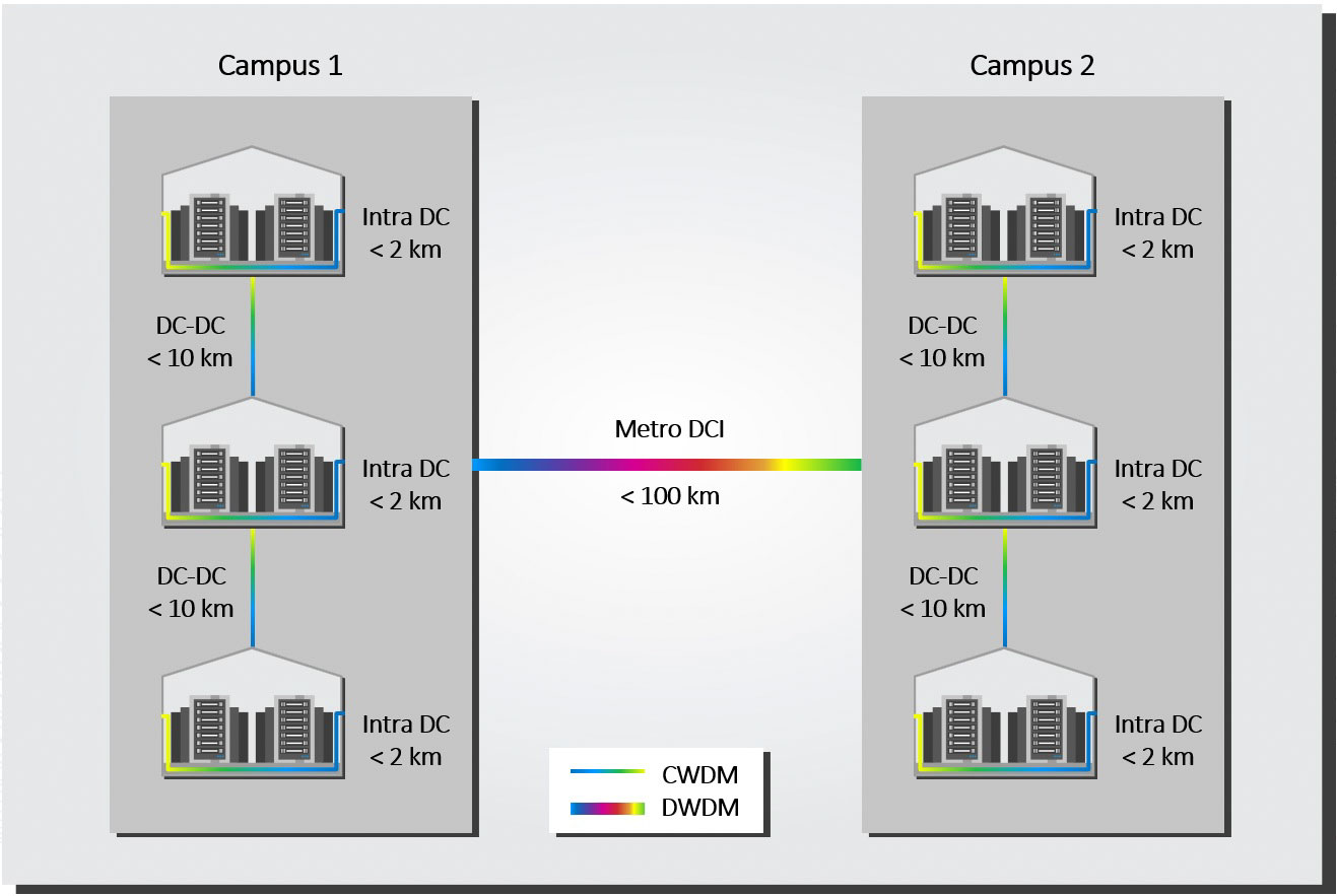
Coherent 400ZR now dominates the metro DCI space, but in the coming decade, coherent technology could also play a role in shorter ranges, such as campus and intra-data center interconnects. As interconnects upgrade to Terabit speeds, coherent technology might start coming closer to direct detect power consumption and cost.
The advances in electronic and photonic integration allowed coherent technology for metro DCIs to be miniaturized into QSFP-DD and OSFP form factors. This progress allowed the Optical Internetworking Forum (OIF) to create a 400ZR multi-source agreement. With small enough modules to pack a router faceplate densely, the datacom sector could profit from a 400ZR solution for high-capacity data center interconnects of up to 80km. Operations teams found the simplicity of coherent pluggables very attractive. There was no need to install and maintain additional amplifiers and compensators as in direct detection: a single coherent transceiver plugged into a router could fulfill the requirements.
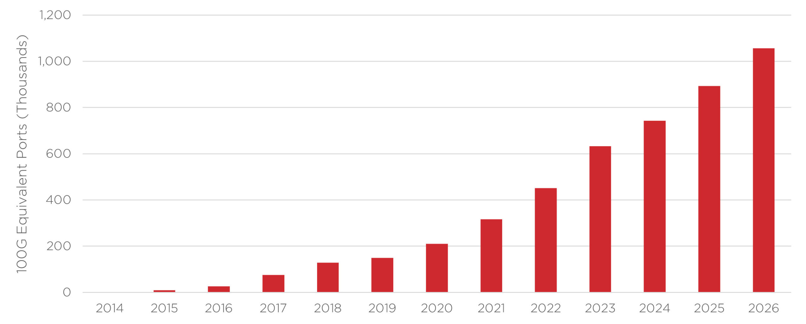
As an example of their success, Cignal AI forecasted that 400ZR shipments would dominate edge applications, as shown in Figure 2.
The campus DCI segment, featuring distances below 10 kilometers, was squarely in the domain of direct detect products when the standard speed of these links was 100Gbps. No amplifiers nor compensators were needed for these shorter distances, so direct detect transceivers are as simple to deploy and maintain as coherent ones.
However, as link bandwidths increase into the Terabit space, these direct detect links will need more amplifiers to reach 10 kilometers, and their power consumption will approach that of coherent solutions. The industry initially predicted that coherent solutions would be able to match the power consumption of PAM4 direct detect solutions as early as 800G generation. However, PAM4 developers have proven resourceful and have borrowed some aspects of coherent solutions without fully implementing a coherent solution. For example, ahead of OFC 2023, semiconductor solutions provider Marvell announced a 1.6Tbps PAM4 platform that pushes the envelope on the cost and power per bit they could offer in the 10 km range.
Following the coming years and how the PAM-4 industry evolves will be interesting. How many (power-hungry) features of coherent solutions will they have to borrow if they want to keep up in upcoming generations and speeds of 3.2 Tbps and beyond? Lumentum’s Chief Technology Officer, Brandon Collings, has some interesting thoughts on the subject in this interview with Gazettabyte.
Below Terabit speeds, direct detect technology (both NRZ and PAM-4) will likely dominate the intra-DCI space (also called data center fabric) in the coming years. In this space, links span less than 2 kilometers, and for particularly short links (< 300 meters), affordable multimode fiber (MMF) is frequently used.
Nevertheless, moving to larger, more centralized data centers (such as hyperscale) is lengthening intra-DCI links. Instead of transferring data directly from one data center building to another, new data centers move data to a central hub. So even if the building you want to connect to might be 200 meters away, the fiber runs to a hub that might be one or two kilometers away. In other words, intra-DCI links are becoming campus DCI links requiring their single-mode fiber solutions.
On top of these changes, the upgrades to Terabit speeds in the coming decade will also see coherent solutions more closely challenge the power consumption of direct detect transceivers. PAM-4 direct detect transceivers that fulfill the speed requirements require digital signal processors (DSPs) and more complex lasers that will be less efficient and affordable than previous generations of direct detect technology. With coherent technology scaling up in volume and having greater flexibility and performance, one can argue that it will also reach cost-competitiveness in this space.
Unsurprisingly, using coherent or direct detect technology for data center interconnects boils down to reach and capacity needs. 400ZR coherent is already established as the solution for metro DCIs. In campus interconnects of 10 km or less, PAM-4 products remain a robust solution up to 1.6 Tbps, but coherent technology is making a case for its use. Thus, it will be interesting to see how they compete in future generations and 3.2 Tbps.
Coherent solutions are also becoming more competitive as the intra-data center sector moves into higher Terabit speeds, like 3.2Tbps. Overall, the datacom sector is moving towards coherent technology, which is worth considering when upgrading data center links.
Tags: 800G, access networks, coherent, cost, cost-effective, Data center, distributed computing, edge and metro DCIs, integration, Intra DCI, license, metro, miniaturized, photonic integration, Photonics, pluggable, power consumption, power consumption SFP, reach, Terabit© 2026 EFFECT PHOTONICS All rights reserved. T&C of Website - T&C of Purchase - Privacy Policy - Cookie Policy - Supplier Code of Conduct