– optics.org

– optics.org

– 거제인터넷방송 GİB

– SemiconductorToday

– The PIC features support for 100G, 400G and 800G ZR applications and will become…
– The PIC features support for 100G, 400G and 800G ZR applications and will become the cornerstone of the smallest tunable laser assembly for coherent applications.
EFFECT Photonics, a leading developer of highly integrated optical solutions, announced today the verification of its fully integrated tunable laser InP-based Photonic Integrated Circuit (PIC), the core enabler powering its digital Pico Integrated Tunable Laser Assembly (pITLA). Tunable lasers are a core component of coherent optical systems enabling Dense Wavelength Division Multiplexing (DWDM), which allows network operators to expand their network capacity without expanding the existing fiber infrastructure. With this milestone, the tunable laser InP-based Photonic Integrated Circuit (PIC) has successfully passed a series of tests showing required performance items outlined by IEEE Std. 802.3-2022, 100GBASE-ZR.
Unlike tunable laser assemblies currently available, the core of EFFECT Photonics digital pITLA is a tunable laser implemented fully as a monolithic integrated InP PIC. This enables advantages such as the ability to achieve a compact footprint, higher assembly yields, and ease of integration into pluggable form factors. The InP PIC is the only solution to integrate the gain section, laser cavity, optical amplifier, and wavelength locker into one chip. By incorporating these functions on a single chip and including the control functions in the assembly, the user can easily communicate and control the laser by simply providing digital commands.
“In the last decade, the industry has made impressive strides in reducing the size of crucial coherent optical functions, making way for digital coherent modules. EFFECT Photonics pITLA sets a new precedent in photonic integration by eliminating the need for external micro-optics for control of tunable lasers,” said Roberto Marcoccia, CEO of EFFECT Photonics. “Our monolithic approach maintains all vital functions while drastically reducing the device’s overall size to a smaller form factor previously unattainable.”
Purposely designed to simplify the design of small form factor pluggables, the integrated InP PIC is the foundation of EFFECT Photonics new pITLA, providing an outstanding blend of power, cost-effectiveness, and compactness. It paves the way for the effortless and cost-efficient design of coherent pluggables, opening up new possibilities for the industry.
To learn more about the EFFECT Photonics pITLA, visit Stand 547 at ECOC23 or attend EFFECT Photonics’ Market Focus Session “Power and Integration: InP for Coherent Transceivers at the Network Edge” on Monday, October 2 at 12pm.
Roberto Marcoccia, CEO of EFFECT PhotonicsIn the last decade, the industry has made impressive strides in reducing the size of crucial coherent optical functions, making way for digital coherent modules. EFFECT Photonics pITLA sets a new precedent in photonic integration by eliminating the need for external micro-optics for control of tunable lasers. Our monolithic approach maintains all vital functions while drastically reducing the device’s overall size to a smaller form factor previously unattainable.
Purposely designed to simplify the design of small form factor pluggables, the integrated InP PIC is the foundation of EFFECT Photonics new pITLA, providing an outstanding blend of power, cost-effectiveness, and compactness. It paves the way for the effortless and cost-efficient design of coherent pluggables, opening up new possibilities for the industry.
To learn more about the EFFECT Photonics pITLA, visit Stand 547 at ECOC23 or attend EFFECT Photonics’ Market Focus Session “Power and Integration: InP for Coherent Transceivers at the Network Edge” on Monday, October 2 at 12pm.
Where Light Meets Digital – EFFECT Photonics is a highly vertically integrated, independent optical systems company addressing the need for high-performance, affordable optic solutions driven by the ever-increasing demand for bandwidth and faster data transfer capabilities. Using our company’s field-proven digital signal processing and forward error correction technology and ultra-pure light sources, we offer compact form factors with seamless integration, cost efficiency, low power, and security of supply. By leveraging established microelectronics ecosystems, we aim to make our products affordable and available in high volumes to address the challenges in 5G and beyond, access-ready coherent solutions, and cloud and cloud edge services. For more information, please visit: www.effectphotonics.com. Follow EFFECT Photonics on LinkedIn and Twitter.
# # #
Media Contact:
Colleen Cronin
EFFECT Photonics
colleencronin@effectphotonics.com

EFFECT Photonics’ coherent technology portfolio has grown in the last two years, including coherent transceivers,…
EFFECT Photonics’ coherent technology portfolio has grown in the last two years, including coherent transceivers, laser sources, and digital signal processors. To lead this portfolio, EFFECT Photonics has hired Charlie Fu as our new Coherent Product Manager. To give you more insight into our new colleague and what drives him, we asked him a few questions.
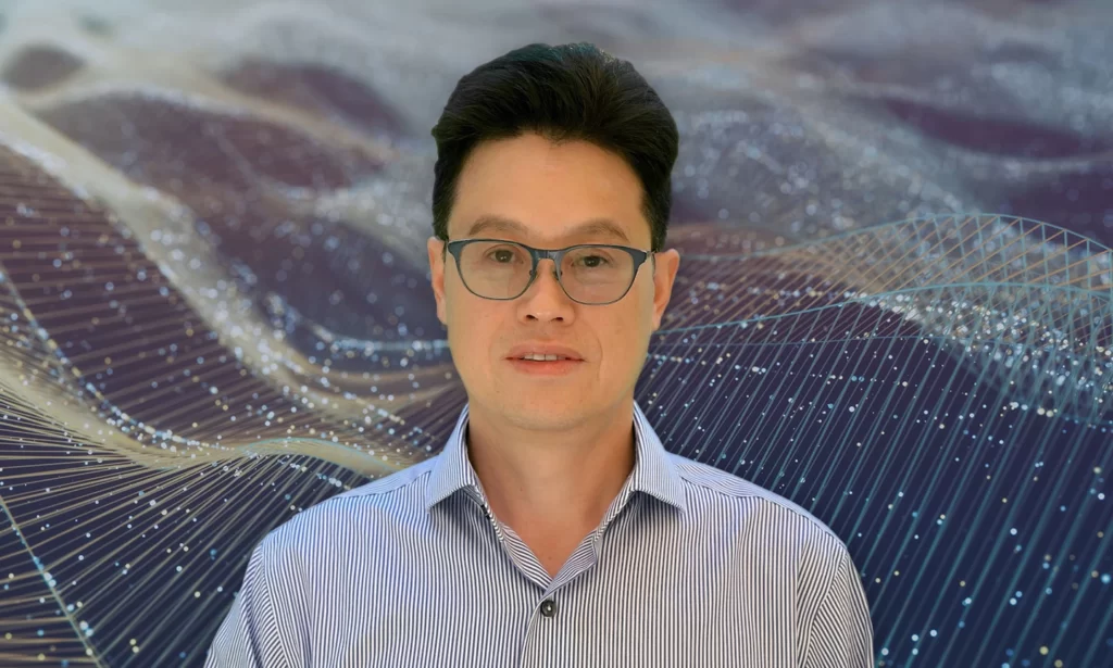
So, my whole life is actually devoted to photonics. When I was a student in college, I studied optoelectronics, and my undergraduate project was doing a diode laser response curve. I also worked hard in graduate school with my supervisor in the lab to test coherent lasers back in the early 1990s when this technology was in its early stages. Back then, the laser was based on bulk micro-optics and could transmit for maybe 10 kilometers of distance. It was a significantly bigger package than now.
I was very lucky to start my career during an optical communications boom, working on fiber optic devices and modules with JDS Uniphase. I built my career there, starting with optical design and a lot of learning.
I then moved to a network company, Nortel Networks, designing links for long-haul transmission systems. We ensured the performance of the optical system and how to specify all the optical components modules to ensure the required performance. Nortel had a very ambitious project at the time. It was a technology challenge of transmitting 40G long haul transmission. Perhaps too ambitious, the year 2000 was perhaps too early still to go coherent.
So yeah, my whole career has been devoted to optics. From working as a hardware design engineer and learning all the optical transponder optical module design. Working with a few well-known brands such as Oclaro.
So I think EFFECT Photonics has a good combination of people and technology, with many interesting technology innovations. The entrepreneurial drive to achieve success.
What attracted me the most was the core technology message of where light meets digital. If we look around, quite a lot of companies have photonics technology OR digital signal processing (DSP) technology. But almost no one has both IP for DSP and photonic technology. Having those IPs puts EFFECT Photonics in a very unique, prestigious position.
I still believe coherent technology is in its infant stage in its application to optical communication. There are still a lot of things to do. For example, moving it to access network communications instead of just long haul. That’s something EFFECT Photonics wants to do and why I’m very excited about the future of our coherent optics.
The coherent system implementation may have changed a lot and gotten smaller, but the technology, the core concept, it’s still exactly the same as 30 years ago. I want to help develop these new systems with the new technology available to optics in the semiconductor sector.
I’m very excited to develop products that use these new technologies, hence why I am now in a Product Manager position.
I’m very excited to leverage my experience and knowledge and I’m very confident I can make a positive contribution to EFFECT Photonics in product design and development.
Tags: Access Network Communication, Charlie Fu, coherent, Coherent Product Manager, Core Technology Message, digital signal processing (DSP), EFFECT Photonics, Entrepreneurial Drive, Fiber Optic Devices, Innovative Technology, Integrated Photonics, IP for DSP and Photonic Technology, Long-Haul Transmission, Optical Communication, Optical Design, Optical Module Design, Optical Transponder, Photonic Technology, Photonics, Photonics Technology, Product Design, Product Development, Semiconductor Sector
Join EFFECT Photonics from October 2nd-4th, 2023 at ECOC Exhibition in Sec, Glasgow, Scotland. ECOC is the largest optical communications exhibition in Europe and a key meeting place for decision-makers. Come and discover firsthand how our technology is transforming where light meets digital, visit booth #547 to learn how EFFECT Photonics’ full portfolio of optical building blocks are enabling 100G coherent to the network edge and next-generation applications.
Build Your Own 100G ZR Coherent Module
At this year’s ECOC, see how easy and affordable it can be to upgrade existing 10G links to a more scalable 100G coherent solution! Try your hand at constructing a 100G ZR coherent module specifically designed for the network edge utilizing various optical building blocks including tunable lasers, DSPs and optical subassemblies.
Tune Your Own PIC (Photonic Integrated Circuit)
Be sure to stop by stand #547 to tune your own PIC with EFFECT Photonics technology. In this interactive and dynamic demonstration, participants can explore first-hand the power of EFFECT Photonics solutions utilizing various parameters and product configurations.
Our experts are also available to discuss customer needs and how EFFECT Photonics might be able to assist. To schedule a meeting, please email marketing@effectphotonics.com
Tags: 100 ZR, 100G, 100gcoherent, access, access networks, bringing100Gtoedge, cloud, cloudedge, coherent, coherentoptics, datacenters, DSP, DSPs, ECOC, ECOC2023, EFFECT Photonics, Integrated Photonics, networkedge, opticcommunications, Optics, photonic integration, Photonics, PIC, tunablelasers, wherelightmeetsdigital
– Link Magazine

Article first published 27 September 2021, updated 31st May 2023. The demand for data and…
Article first published 27 September 2021, updated 31st May 2023.
The demand for data and other digital services is rising exponentially. From 2010 to 2020, the number of Internet users worldwide doubled, and global internet traffic increased 12-fold. By 2022, internet traffic had doubled yet again. While 5G standards are more energy-efficient per bit than 4G, the total power consumption will be much higher than 4G. Huawei expects that the maximum power consumption of one of their 5G base stations will be 68% higher than their 4G stations. These issues do not just affect the environment but also the bottom lines of communications companies.
Keeping up with the increasing data demand of future networks sustainably will require operators to deploy more optical technologies, such as photonic integrated circuits (PICs), in their access and fronthaul networks.
Lately, we have seen many efforts to increase further the integration on a component level across the electronics industry. For example, moving towards greater integration of components in a single chip has yielded significant efficiency benefits in electronics processors. Apple’s recent M1 and M2 processors integrate all electronic functions in a single system-on-chip (SoC) and consume significantly less power than the processors with discrete components used in their previous generations of computers.
| 𝗠𝗮𝗰 𝗠𝗶𝗻𝗶 𝗠𝗼𝗱𝗲𝗹 | 𝗣𝗼𝘄𝗲𝗿 𝗖𝗼𝗻𝘀𝘂𝗺𝗽𝘁𝗶𝗼𝗻 | |
| 𝗜𝗱𝗹𝗲 | 𝗠𝗮𝘅 | |
| 2023, M2 | 7 | 5 |
| 2020, M1 | 7 | 39 |
| 2018, Core i7 | 20 | 122 |
| 2014, Core i5 | 6 | 85 |
| 2010, Core 2 Duo | 10 | 85 |
| 2006, Core Solo or Duo | 23 | 110 |
| 2005, PowerPC G4 | 32 | 85 |
| Table 1: Comparing the power consumption of a Mac Mini with an M1 and M2 SoC chips to previous generations of Mac Minis. [Source: Apple’s website] | ||
Photonics is also achieving greater efficiency gains by following a similar approach to integration. The more active and passive optical components (lasers, modulators, detectors, etc.) manufacturers can integrate on a single chip, the more energy they can save since they avoid coupling losses between discrete components and allow for interactive optimization.
Let’s start by discussing three different levels of device integration for an optical device like a transceiver:
While discrete builds and partial integration have advantages in managing the production yield of the individual components, full integration leads to fewer optical losses and more efficient packaging and testing processes, making them a much better fit in terms of sustainability.
The interconnects required to couple discrete components result in electrical and optical losses that must be compensated with higher transmitter power and more energy consumption. The more interconnects between different components, the higher the losses become. Discrete builds will have the most interconnect points and highest losses. Partial integration reduces the number of interconnect points and losses compared to discrete builds. If these components are made from different optical materials, the interconnections will suffer additional losses.
On the other hand, full integration uses a single chip of the same base material. It does not require lossy interconnections between chips, minimizing optical losses and significantly reducing the energy consumption and footprint of the transceiver device.

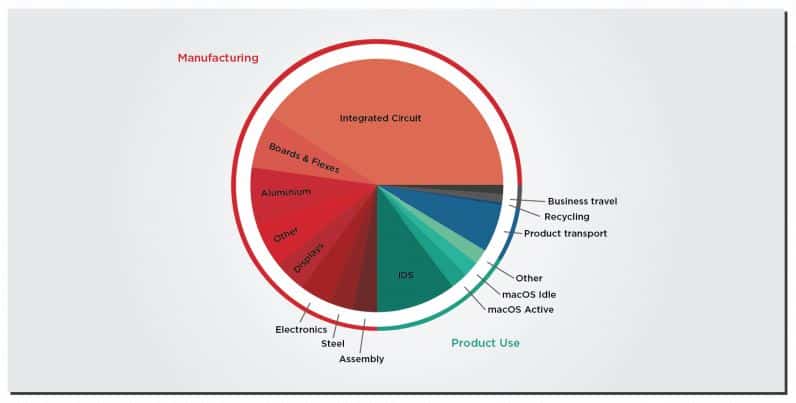
When it comes to energy consumption and sustainability, we shouldn’t just think about the energy the PIC consumes but also the energy and carbon footprint of fabricating the chip and assembling the transceiver. To give an example from the electronics sector, a Harvard and Facebook study estimated that for Apple, manufacturing accounts for 74% of their carbon emissions, with integrated circuit manufacturing comprising roughly 33% of Apple’s carbon output. That’s higher than the emissions from product use.
Testing is another aspect of the manufacturing process that impacts sustainability. The earlier faults can be found in the testing process, the greater the impact on the use of materials and the energy used to process defective chips. Ideally, testing should happen not only on the final, packaged transceiver but in the earlier stages of PIC fabrication, such as measuring after wafer processing or cutting the wafer into smaller dies.
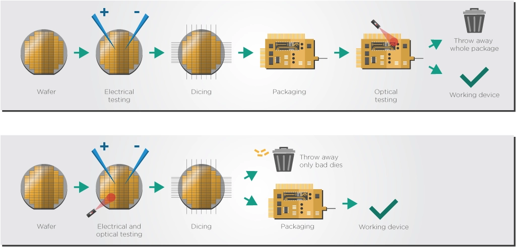
Discrete and partial integration approaches do more of their optical testing on the finalized package, after connecting all the different components together. Should just one of the components not pass the testing process, the complete packaged transceiver would need to be discarded, potentially leading to a massive waste of materials as nothing can be ”fixed” or reused at this stage of the manufacturing process.
Full integration enables earlier optical testing on the semiconductor wafer and dies. By testing the dies and wafers directly before packaging, manufacturers need only discard the bad dies rather than the whole package, which saves valuable energy and materials.
While communication networks have become more energy-efficient, further technological improvements must continue decreasing the cost of energy per bit and keeping up with the exponential increase in Internet traffic. At the same time, a greater focus is being placed on the importance of sustainability and responsible manufacturing. All the photonic integration approaches we have touched on will play a role in reducing the energy consumption of future networks. However, out of all of them, only full integration is in a position to make a significant contribution to the goals of sustainability and environmentally friendly manufacturing. A fully integrated system-on-chip minimizes optical losses, transceiver energy consumption, power usage, and materials wastage while at the same time ensuring increased energy efficiency of the manufacturing, packaging, and testing process.
Tags: ChipIntegration, Data demand, DataDemand, EFFECT Photonics, Energy consumption reduction, energy efficiency, EnergySavings, Environmental impact, Fully Integrated PICs, Green Future, GreenFuture, Integrated Photonics, Integration benefits, Manufacturing sustainability, Optical technologies, OpticalComponents, photonic integration, PIC, PICs, ResponsibleManufacturing, sustainability telecommunication, Sustainable, Sustainable future, SustainableNetworks, Transceiver optimization
Photonics is one of the enabling technologies of the future. Light is the fastest information…
Photonics is one of the enabling technologies of the future. Light is the fastest information carrier in the universe and can transmit this information while dissipating less heat and energy than electrical signals. Thus, photonics can dramatically increase the speed, reach, and flexibility of communication networks and cope with the ever-growing demand for more data. And it will do so at a lower energy cost, decreasing the Internet’s carbon footprint. Meanwhile, fast and efficient photonic signals have massive potential for sensing and imaging applications in medical devices, automotive LIDAR, agricultural and food diagnostics, and more.
Given its importance, we should discuss the fabrication processes inside photonic semiconductor foundries.
Manufacturing semiconductor chips for photonics and electronics is one of the most complex procedures in the world. For example, back in his university days, EFFECT Photonics co-founder Boudewijn Docter described a fabrication process with 243 steps!
Yuqing Jiao, Associate Professor at the Eindhoven University of Technology (TU/e), explains the fabrication process in a few basic, simplified steps:
Real life is, of course, a lot more complicated and will require cycling through these steps tens of times, leading to processes with more than 200 total steps. Let’s go through these basic steps in a bit more detail.
1. Layer Epitaxy and Deposition: Different chip elements require different semiconductor material layers. These layers can be grown on the semiconductor wafer via a process called epitaxy or deposited via other methods, such as physical or chemical vapor deposition.
2. Lithography (i.e., printing): There are a few lithography methods, but the one used for high-volume chip fabrication is projection optical lithography. The semiconductor wafer is coated with aphotosensitive polymer film called a photoresist. Meanwhile, the design layout pattern is transferred to an opaque material called a mask. The optical lithography system projects the mask pattern onto the photoresist. The exposed photoresist is then developed (like photographic film) to complete the pattern printing.
3. Etching: Having “printed” the pattern on the photoresist, it is time to remove (or etch) parts of the semiconductor material to transfer the pattern from the resist into the wafer. Etching techniques can be broadly classified into two categories.
4. Cleaning and Surface Preparation: After etching, a series of steps will clean and prepare the surface before the next cycle.
Figure 5 summarizes how an InP photonic device looks after the steps of layer epitaxy, etching, dielectric deposition and planarization, and metallization.
After this fabrication process ends, the processed wafers are shipped worldwide to be tested and packaged into photonic devices. This is an expensive process we discussed in one of our previous articles.
The process of making photonic integrated circuits is incredibly long and complex, and the steps we described in this article are a mere simplification of the entire process. It requires tremendous knowledge in chip design, fabrication, and testing from experts in different fields worldwide. EFFECT Photonics was founded by people who fabricated these chips themselves, understood the process intimately and developed the connections and network to develop cutting-edge PICs at scale.
Tags: Agricultural, Carbon Footprint, Chip Material, Cleaning, Communication Networks, Deposition, Energy Cost, Epitaxy, Etching, Fabrication Process, Food Diagnostics, Integrated Photonics, LIDAR, Lithography, Manufacturing, Medical Devices, Metallization, Photonic Foundry, Photonics, Semiconductor, Sensing and Imaging, Surface Preparation
Today’s digital society depends heavily on securely transmitting and storing data. One of the oldest…
Today’s digital society depends heavily on securely transmitting and storing data. One of the oldest and most widely used methods to encrypt data is called RSA (Rivest-Shamir-Adleman – the surnames of the algorithm’s designers). However, in 1994 mathematician Peter Shor proved that an ideal quantum computer could find the prime factors of large numbers exponentially more quickly than a conventional computer and thus break RSA encryption within hours or days.
While practical quantum computers are likely decades away from implementing Shor’s algorithm with enough performance and scale to break RSA or similar encryption methods, the potential implications are terrifying for our digital society and our data safety.
Given these risks, arguably the most secure way to protect data and communications is by fighting quantum with quantum: protect your data from quantum computer hacking by using security protocols that harness the power of quantum physics laws. That’s what quantum key distribution (QKD) does.
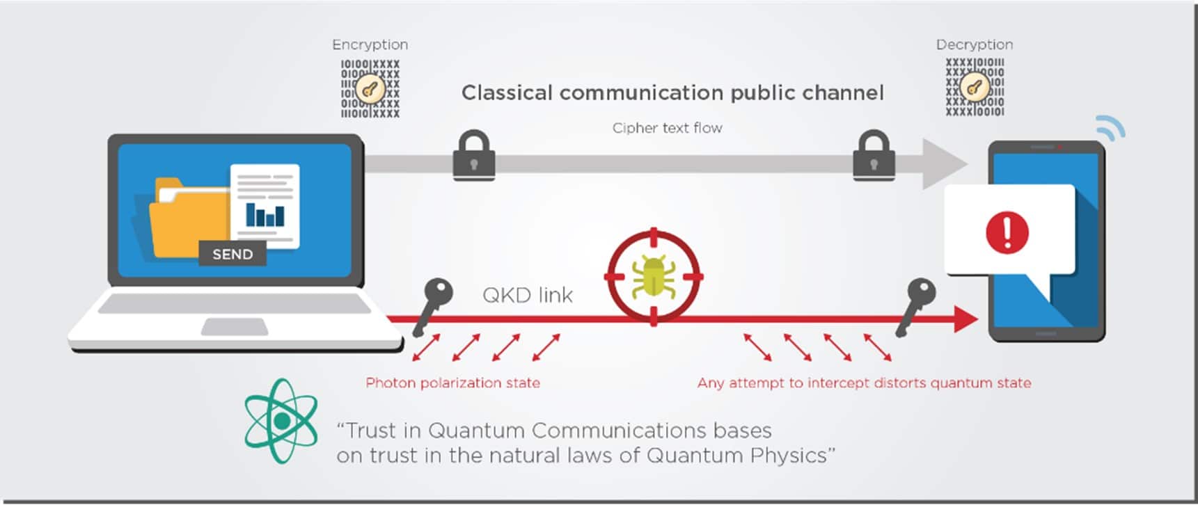
The quantum bits (qubits) used by QKD systems can be photons, electrons, atoms, or any other system that can exist in a quantum state. However, using photons as qubits will likely dominate the quantum communications and QKD application space. We have decades of experience manipulating the properties of photons, such as polarization and phase, to encode qubits. Thanks to optical fiber, we also know how to send photons over long distances with relatively little loss. Besides, optical fiber is already a fundamental component of modern telecommunication networks, so future quantum networks can run on that existing fiber infrastructure. All these signs point towards a new era of quantum photonics.
Photonic QKD devices have been, in some shape or form, commercially available for over 15 years. Still, factors such as the high cost, large size, and the inability to operate over longer distances have slowed their widespread adoption. Many R&D efforts regarding quantum photonics aim to address the size, weight, and power (SWaP) limitations. One way to overcome these limitations and reduce the cost per device would be to integrate every QKD function—generating, manipulating, and detecting photonic qubits—into a single chip.
Bringing quantum products from lab prototypes to fully realized products that can be sold on the market is a complex process that involves several key steps.
One of the biggest challenges in bringing quantum products to market is scaling up the technology from lab prototypes to large-scale production. This requires the development of reliable manufacturing processes and supply chains that can produce high-quality quantum products at scale. Quantum products must be highly performant and reliable to meet the demands of commercial applications. This requires extensive testing and optimization to ensure that the product meets or exceeds the desired specifications.
In addition, quantum products must comply with relevant industry standards and regulations to ensure safety, interoperability, and compatibility with existing infrastructure. This requires close collaboration with regulatory bodies and industry organizations to develop appropriate standards and guidelines.
Photonic integration is a process that makes these goals more attainable for quantum technologies. By taking advantage of existing semiconductor manufacturing systems, quantum technologies can more scale up their production volumes more easily.
One of the most significant advantages of integrated photonics is its ability to miniaturize optical components and systems, making them much smaller, lighter, and more portable than traditional optical devices. This is achieved by leveraging micro- and nano-scale fabrication techniques to create optical components on a chip, which can then be integrated with other electronic and optical components to create a fully functional device.
The miniaturization of optical components and systems is essential for the development of practical quantum technologies, which require compact and portable devices that can be easily integrated into existing systems. For example, compact and portable quantum sensors can be used for medical imaging, geological exploration, and industrial process monitoring. Miniaturized quantum communication devices can be used to secure communication networks and enable secure communication between devices.
Integrated photonics also allows for the creation of complex optical circuits that can be easily integrated with other electronic components, to create fully integrated opto-electronic quantum systems. This is essential for the development of practical quantum computers, which require the integration of a large number of qubits (quantum bits) with control and readout electronics.
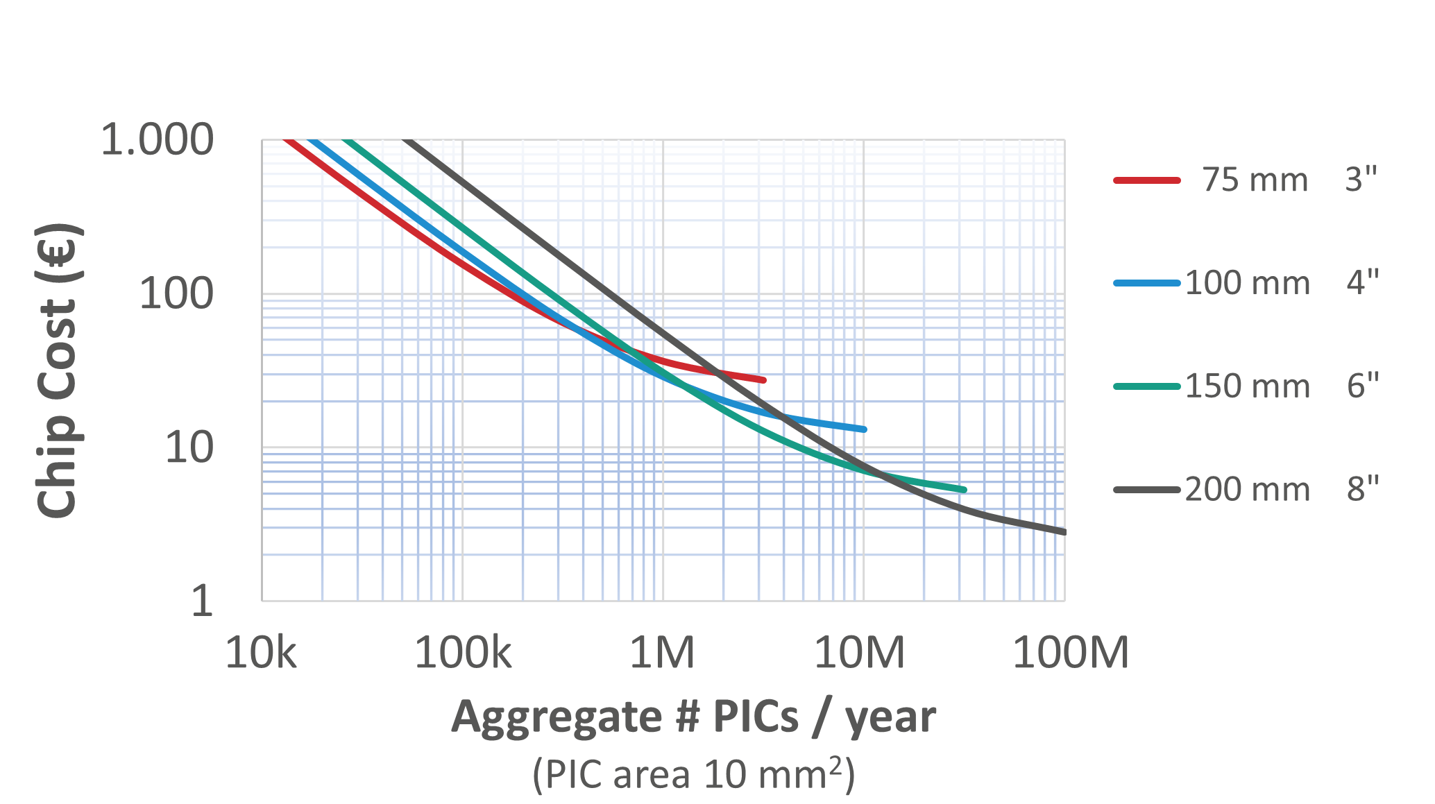
Wafer scale photonics manufacturing demands a higher upfront investment, but the resulting high-volume production line drives down the cost per device. This economy-of-scale principle is the same one behind electronics manufacturing, and the same must be applied to photonics. The more optical components we can integrate into a single chip, the more can the price of each component decrease. The more optical System-on-Chip (SoC) devices can go into a single wafer, the more can the price of each SoC decrease.
Researchers at the Technical University of Eindhoven and the JePPIX consortium have done some modelling to show how this economy of scale principle would apply to photonics. If production volumes can increase from a few thousands of chips per year to a few millions, the price per optical chip can decrease from thousands of Euros to mere tens of Euros. This must be the goal for the quantum photonics industry.
By integrating all optical components on a single chip, we also shift the complexity from the assembly process to the much more efficient and scalable semiconductor wafer process. Assembling and packaging a device by interconnecting multiple photonic chips increases assembly complexity and costs. On the other hand, combining and aligning optical components on a wafer at a high volume is much easier, which drives down the device’s cost.
Overall, bringing quantum products to market requires a multi-disciplinary approach that involves collaboration between scientists, engineers, designers, business professionals, and regulatory bodies to develop and commercialize a high-quality product that meets the needs of its target audience. Integrated photonics offers significant advantages in miniaturization and scale-up potential, which are essential in taking quantum technologies from the lab to the market.
Tags: Economy-of-scale, EFFECT Photonics, Integrated Photonics, miniaturization, Photonics, Photons, Quantum, Quantum products, Qubits, RSA encryption, Wafer Scale Photonics© 2025 EFFECT PHOTONICS All rights reserved. T&C of Website - T&C of Purchase - Privacy Policy - Cookie Policy - Supplier Code of Conduct