Photonic System-on-Chip is the Future
Before 2020, Apple made its computer processors with discrete components. In other words, electronic components were manufactured on separate chips, and then these chips were assembled into a single package. However, the interconnections between the different chips produced losses and incompatibilities that made the device less efficient. After 2020, starting with Apple’s M1 processor, they now fully integrate all components on a single chip, avoiding losses and incompatibilities.
Apple’s fully integrated processor consumes a third of the power and lower costs than their older processors while still providing similar performance. EFFECT Photonics does something similar to what Apple did, but with optical components instead of electronic components. By integrating all the optical components (lasers, detectors, modulators, etc.) in a single system on a chip, we can minimize the losses and make the device more efficient. This approach is what we call photonic System-on-Chip (SoC).

By integrating all optical components on a single chip, we also shift the complexity from the assembly process to the much more efficient and scalable semiconductor wafer process. Assembling and packaging a device by interconnecting multiple photonic chips increases assembly complexity and costs. On the other hand, combining and aligning optical components on a wafer at a high volume is much easier, which drives down the device’s cost. Testing is another aspect that becomes more efficient and scalable when manufacturing at the wafer level.
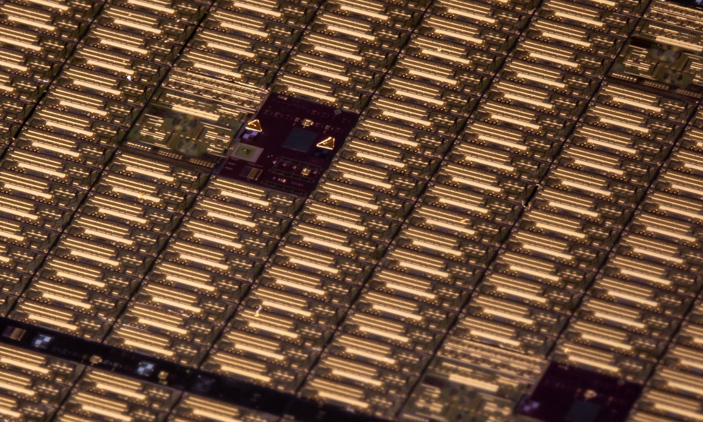
When faults are found earlier in the testing process, fewer resources and energy are spent processing defective chips. Ideally, testing should happen not only on the final, packaged transceiver but in the earlier stages of photonic SoC fabrication, such as measuring after wafer processing or cutting the wafer into smaller dies. Full photonic integration enables earlier optical testing on the semiconductor wafer and dies. By testing the dies and wafers directly before packaging, manufacturers need only discard the bad dies rather than the whole package, which saves time, and cost and is more energy-efficient and sustainable.

For example, EFFECT Photonics reaps these benefits in its production processes. 100% of electrical testing on the photonic SoCs happens at the wafer level, and our unique integration technology allows for 90% of optical testing on the wafer. The real-world applications of SoCs are practically limitless and priceless. Electronic SoCs are used in most, if not all, portable devices, such as smartphones, cameras, tablets, and other wireless technologies. SoCs are also frequently used in equipment involved in the Internet of Things, embedded systems, and, of course, photonics. Data center interconnects are an excellent example of an application that benefits from a photonic SoC approach. As DCIs demand higher performance and reach, it’s no longer sufficient to have a solution that integrates just some parts of a system.
That is why EFFECT Photonics’ business strategy aims to solve the interconnect challenges through a holistic photonic SoC approach that understands the interdependence of system elements. By combining the photonic SoC with highly optimized packaging with cost-effective electronics, we are building a high production volume platform that can meet the demands of the datacom sector.