Access to information at our finger tips powered by integrated chips
We all love watching the latest House of Cards on our cellphones or tablets, navigating the streets of Barcelona while listening to music through our apps – preferably without any delays or hiccups. With all this new, mobile technology in our hands, our thirst for fast connections and lots of data has grown exponentially. But data technology is reaching its limits. What we need is nothing short of a revolutionary innovation that is able to deal with more data at the speed of light.
Some 50 years ago, optical fibers were the answer to our growing need for fast data. They span from country to country, crossing the oceans and forming the largest piece of man-made infrastructure that exists on our planet today. By using Wavelength Division Multiplexing (WDM), telecommunications companies worldwide were able to quickly expand the capacity of their networks through the use of different wavelengths of laser light that feed lots of separate signals over a single strand of optical fiber. Thanks to these inventions and immense technological innovations in our computers, mobile devices, and new applications, within a few decades our need for even faster data rates continue.
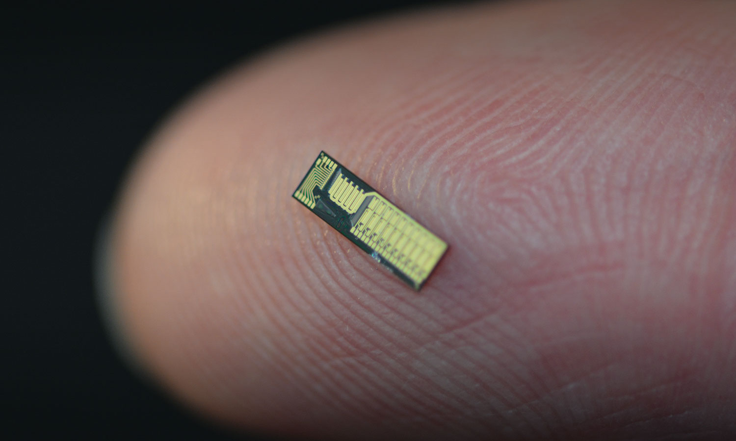
Unfortunately, the capacity of the current generation of optical devices hasn’t kept pace. Not only on-demand video streaming is to blame, but also the development of ‘The Internet of Things’ and advanced machine-to-machine communication will demand stable, secure, yet inexpensive solutions. This is where integrated photonic chips plays an important part; optical chips that can send and receive multiple light signals simultaneously, all within the same physical size as a chocolate bar.
EFFECT Photonics, a spin-off from the Technical University of Eindhoven (TU/e), saw a strong market need to bring its ‘Optical System-on-Chip’ technology to market in order to meet the soaring demand for bandwidth in cell towers and between data centers. EFFECT Photonics develops and delivers highly integrated optical components based on InP (Indium Phosphide), the material of choice for combining efficient laser light sources, waveguides, modulators, amplifiers, and photodiodes used in optical communication systems throughout the world. In 2013 they started building a demonstration model for this Dense Wavelength Division Multiplexing (DWDM) optical system based on integrated photonics, working closely with their customers such as data centers and telcos to define their requirements.
Each photonic chip can handle huge bandwidths of data in a far more condensed, energy efficient and cost-effective way than current optical devices. EFFECT Photonics’ current design improves the port density by a factor of 5 while lowering operational costs by up to 40%. Due to the exponential growth in data in the forthcoming years by a factor of 10, experts foresee a huge rise in energy demand from data centers and telecommunication services. Our current energy use while surfing the Internet already makes up 5% of all energy consumption worldwide, by 2020 this will be 20%. EFFECT Photonics’ ‘Optical System-on-Chip’ technology might just be the tipping point for Obama’s Climate Change Plan to succeed.
EFFECT Photonics is scaling up and opened a second facility in the United Kingdom, Torbay in 2015. Scaling up to manufacture in volume can be a complex challenge, however, EFFECT Photonics has set out to design for low cost manufacturing from the very beginning. Working together with several photonic innovators at their doorstep, like the TU/e and SMART Photonics, EFFECT Photonics is taking micro-photonics to a serious macro-economic business.