– LightwaveOnline

⚠️ Website Under Construction
– LightwaveOnline
EFFECT Photonics to Become the Most Highly Vertically Integrated, Independent Coherent Optical Module Vendor San…
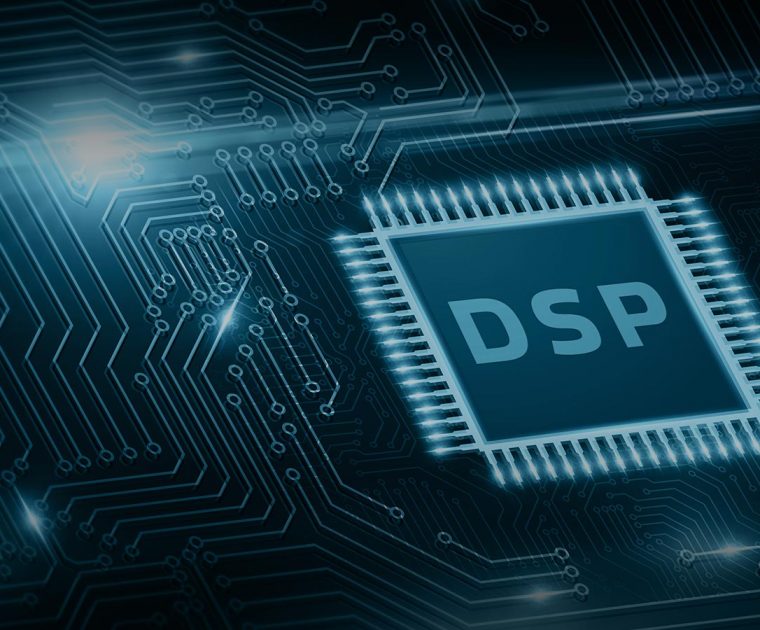
San Diego, United States America – Today at OFC (Optical Fiber Conference) 2022, EFFECT Photonics, a leading provider of highly integrated optical communication products is announcing that it signed a definitive agreement to acquire coherent optical digital signal processing (DSP) and forward error correction (FEC) technology as well as a highly experienced engineering team from global communications company, Viasat Inc. (NASDAQ: VSAT).
Viasat is a long-established player in DSP and FEC technology. With eight generations of design IP, they have a proven track record of delivering successful field deployments.
From this acquisition, EFFECT Photonics will now own the entire coherent technology stack of all optical functions, including a high-performance tunable laser, together with DSP and FEC. This will enable the Company to deliver on its ambition to make high performance coherent communications solutions widely accessible and affordable. Furthermore, it will enable longer term economic and environmentally sustainable communications due to the ability to deliver high-end performance and reach within a small footprint and with lower power consumption. This opens the way to drive coherent technology into new places, revolutionizing the way the world interconnects.
This transaction is expected to provide the following customer benefits:
EFFECT Photonics has also secured an additional $20M in Series-C funding bringing the total to $63M. Additionally, pursuant to the DSP acquisition agreement, Viasat will be joining EFFECT Photonics’ Supervisory Board and hold a minority interest in the Company.
“This is a significant step in accelerating our ambition to make coherent optical communications ubiquitous and further drive our product portfolio growth. We look forward to welcoming the team of highly skilled and experienced design architects and engineers who will be joining us to drive the development of energy efficient, high performance and affordable coherent solutions.
James Regan, CEO EFFECT Photonics.
With all the recent changes in the industry landscape, this means that EFFECT Photonics is the only independent vendor able to deliver both the active optical components and the DSP. This will offer the market more choice and the ability to source superior solutions“
“Given the trend of the fiber optic communications industry towards consolidation to provide vertically integrated end-to-end solutions, we believe that combining Viasat’s assets and capabilities with the unique integrated photonics capabilities of EFFECT Photonics will create substantially more market opportunities and better products. By investing in this Netherlands-headquartered company, we will also further expand our presence in Europe and be able to partner with EFFECT to bring state-of-the-art integrated photonics to Viasat’s own customers.”
Russell Fuerst, business area leader and vice president, Viasat.
–End of press release–
EFFECT Photonics delivers highly integrated optical communications products based on its Dense Wavelength Division Multiplexing (DWDM) optical System-on-Chip technology. The key enabling technology for DWDM systems is full monolithic integration of all photonic components within a single chip and being able to produce these in volume with high yield at low cost. With this capability, EFFECT Photonics is addressing the need for affordable DWDM solutions driven by the soaring demand for high bandwidth connections. EFFECT Photonics is headquartered in The Netherlands, with additional facilities in the UK, the US and Taiwan, and a worldwide network of sales partners. http://www.effectphotonics.com
Viasat is a global communications company that believes everyone and everything in the world can be connected. For more than 35 years, Viasat has helped shape how consumers, businesses, governments and militaries around the world communicate. Today, the Company is developing the ultimate global communications network to power high-quality, secure, affordable, fast connections to impact people’s lives anywhere they are—on the ground, in the air or at sea. To learn more about Viasat, visit: www.viasat.com, go to Viasat’s Corporate Blog, or follow the Company on social media at: Facebook, Instagram, LinkedIn, Twitter or YouTube.
Copyright © 2022 EFFECT Photonics. All rights reserved. Viasat, the Viasat logo and the Viasat signal are registered trademarks of Viasat, Inc. All other product or company names mentioned are used for identification purposes only and may be trademarks of their respective owners.
Tags: acquisition, coherent, coherent communication systems, coherent optical module vendor, DSP, FEC, forward error correction, high vertical integration, independent coherent optical module vendor, Integrated Photonics, optical digital signal processing, optical engine, tunable laser, Viasat
EFFECT Photonics is delighted to announce that it is on the list of 50 most…
EFFECT Photonics is delighted to announce that it is on the list of 50 most promising European Deep Tech start-ups as part of the EIC ScalingUp programme. A Selection Committee of experienced investors chose to include EFFECT Photonics from more than 3,000 candidates in a selection process covering several stages. These companies are considered the most promising EIC (European Innovation Council) deep tech companies that have the potential to achieve substantial growth, and to become world-scale companies or to realise a big exit or IPO.
“Through the EIC ScalingUp project the EIC supports high-growth, high potential companies with visionary ideas, disruptive technologies, and the ambition to grow exponentially in Europe and globally.”– Jean-David Malo, Director, European Innovation Council (EIC) and SMEs Executive Agency (EISMEA).
“We are honoured to be part of this select group. Our thanks go to the European Innovation Council, Tech Tour, DeepWave Ventures, Boston Consulting Group and bpifrance for the opportunity to further expand on our ambitions to make complex, powerful optical systems simpler and more accessible.”– James Regan, CEO EFFEFCT Photonics.
To learn more about the EIC ScalingUp programme, please click here.
To download the Top50 Publication, please click here.
About EFFECT Photonics
EFFECT Photonics delivers highly integrated optical communications products based on its Dense Wavelength Division Multiplexing (DWDM) optical System-on-Chip technology. The key enabling technology for DWDM systems is full monolithic integration of all photonic components within a single chip and being able to produce these in volume with high yield at low cost. With this capability, EFFECT Photonics is addressing the need for low cost DWDM solutions driven by the soaring demand for high bandwidth connections. EFFECT Photonics is headquartered in Eindhoven, The Netherlands, with additional R&D and manufacturing in South West UK, a subsidiary in Taiwan, a facility opening shortly outside Boston, and a worldwide network of sales partners.


Join EFFECT Photonics from March 7 to 9, 2023 at OFC in San Diego, California, the world’s largest event for optical networking and communications, to discover firsthand how our technology is transforming where light meets digital. Visit Booth #2423 to learn how EFFECT Photonics’ full portfolio of optical building blocks are enabling 100G coherent to the network edge and next-generation applications.
Build Your Own 100G ZR Coherent Module
At this year’s OFC, see how easy and affordable it can be to upgrade existing 10G links to a more scalable 100G coherent solution! Try your hand at constructing a 100G ZR coherent module specifically designed for the network edge utilizing various optical building blocks including tunable lasers, DSPs and optical subassemblies.
Tune Your Own PIC (Photonic Integrated Circuit)
Be sure to stop by Booth #2423 to tune your own PIC with EFFECT Photonics technology. In this interactive and dynamic demonstration, participants can explore first-hand the power of EFFECT Photonics solutions utilizing various parameters and product configurations.
Our experts are also available to discuss customer needs and how EFFECT Photonics might be able to assist. To schedule a meeting, please email marketing@effectphotonics.com
Tags: 100 ZR, 100G, 100gcoherent, access, access networks, bringing100Gtoedge, cloud, cloudedge, coherent, coherentoptics, datacenters, DSP, DSPs, EFFECT Photonics, Integrated Photonics, networkedge, ofc23, opticcommunications, Optics, photonic integration, Photonics, PIC, tunablelasers, wherelightmeetsdigital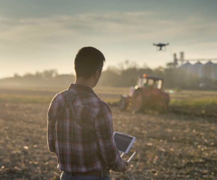
Precision farming is essential in a world with over 10 billion people by 2050 and…
Precision farming is essential in a world with over 10 billion people by 2050 and a food demand that is expanding at an exponential pace. The 2019 World Resources Report from the World Economic Forum warns that at the current level of food production efficiency, feeding the world in 2050 would require “clearing most of the world’s remaining forests, wiping out thousands more species, and releasing enough greenhouse gas emissions to exceed the 1.5°C and 2°C warming targets enshrined in the Paris Agreement – even if emissions from all other human activities were entirely eliminated.”
Technology can help the agrifood industry improve efficiency and meet these demands by combining robotics, machine vision, and small sensors to precisely and automatically determine the care needed by plants and animals in our food supply chain. This approach helps control and optimize food production, resulting in more sustainable crops, higher yields, and safer food.

Sensors based on integrated photonics can enable many of these precision farming applications. Photonic chips are lighter and smaller than other solutions so they can be deployed more easily in these agricultural use cases. The following article will provide examples of how integrated photonics and optical technology can add value to the agriculture and food industries.
The Netherlands is such a small country that if it were a US state, it would be among the ten smallest states, with a land area between West Virginia and Maryland. Despite its size, the Food and Agriculture Organization of the United Nations (FAO) ranked the Netherlands as the second largest exporter of food in the world by revenue in 2020, only behind the Americans and ahead of countries like Germany, China, or Brazil. These nations have tens or hundreds of times more arable land than the Dutch. Technology is a significant reason for this achievement, and the Dutch are arguably the most developed nation in the world regarding precision farming.
The hub of Dutch agrifood research and development is called the Food Valley, centered in the municipality of Wageningen in Gelderland province. In this area, many public and private R&D initiatives are carried out jointly with Wageningen University, a world-renowned leader in agricultural research.
When interviewed last year, Harrij Schmeitz, Director of the Fruit Tech Campus in Geldermalsen, mentions the example of a local fruit supplier called Fruitmasters. They employ basic cameras to snap 140 photographs of each apple that travels through the sorting conveyor, all within a few milliseconds. These photographs are used to automatically create a 3D model and help the conveyor line filter out the rotten apples before they are packaged for customers. This process was done manually in the past, so this new 3D mapping technology significantly improves efficiency.
These techniques are not just constrained to Gelderland, of course. Jacob van den Borne is a potato farmer from Reusel in the province of North Brabant, roughly a half-hour drive from EFFECT Photonics’ Eindhoven headquarters. Van den Borne’s farm includes self-driving AVR harvesters (shown in the video below), and he has been using drones in his farms since 2011 to photograph his fields and study the soil quality and farming yield.
The drone pictures are used to create maps of the fields, which then inform farming decisions. Van den Borne can study the status of the soil before farming, but even after crops have sprouted, he can study which parts of the field are doing poorly and need more fertilization. These measures prevent food waste and the overuse of fertilizer and pesticides. For example, Van den Borne’s farms have eliminated pesticide chemicals in their greenhouses while boosting their yield. The global average yield of potatoes per acre is around nine tons, but his farms yield more than 20 tons per acre!
If you want to know more about Van den Borne and his use of technology and data, you can read this article.
Artificial lighting is a frequent requirement of indoor plant production facilities to increase production and improve crop quality. Growers are turning to LED lighting because it is more efficient than traditional incandescent or fluorescent systems at converting electricity to light. LED lights are made through similar semiconductor manufacturing processes to photonics chips.
LED lighting also provides a greater variety of colors than the usual yellow/orange glow. This technology allows gardeners to pick colors that match each plant’s demands from seedlings through cultivation, unlike high-pressure sodium or other traditional lighting systems. Different colors of visible light create different chlorophyll types in plants, so LED lights can be set to specific colors to provide the best chlorophyll for each development stage.
For example, suppose you roam around the Westland municipality of the Netherlands. You might occasionally catch a purple glow in the night skies, which has nothing to do with UFOs or aliens wanting to abduct you. As explained by Professor Leo Marcelis of Wageningen University (see the above video), researchers have found that red light is very good for plant growth, and mixing it with five to ten percent blue light gives even better results. Red and blue are also the most energy-efficient colors for LEDs, which helps reduce energy consumption even more. As a result, the farmers can save on light and energy use while the environment profits too.
Modern farmers like Jacob van den Borne collect a large quantity of sensor data, which allows them to plan and learn how to provide plants with the perfect amount of water, light, and nutrients at the proper moment. Farmers can use these resources more efficiently and without waste thanks to this sensor information.
For example, Van den Borne uses wireless, Internet-of-Things sensors from companies like Sensoterra (video below) to gauge the soil’s water level. As we speak, researchers in the OnePlanet Research Center, a collaboration including the Imec R&D organization and Wageningen University, are developing nitrogen sensors that run on optical chips and can help keep nitrogen emissions in check.
These sensors will be connected to local servers and the internet for faster data transfer, so many of the issues and photonics solutions discussed in previous articles about the cloud edge and access networks are also relevant for agrifood sensors. Thus, improving optical communication networks will also impact the agrifood industry positively.
In a future of efficient high-tech and precision farming, optics and photonics will play an increasingly important role.
Optical sensors on a chip can be fast, accurate, small, and efficient. They will provide food producers with plenty of data to optimize their production processes and monitor the environmental impact of food production. Novel lighting methods can reduce the energy consumption of greenhouses and other indoor plant facilities. Meanwhile, photonics will also be vital to improving the capacity of the communications networks that these sensors run in.
With photonics-enabled precision processes, the agrifood industry can improve yields and supply, optimize resource use, reduce waste throughout the value chain, and minimize environmental impact.
Tags: atmosphere, demand, emissions, energy consumption, environment, future, high tech farming, high volume, Integrated Photonics, population growth, Precision agriculture, precision farming, process, resource, sensors, supply, waste
It seems like everybody agrees that photonics is one of the most promising sectors for…
It seems like everybody agrees that photonics is one of the most promising sectors for high-tech advancement. In this case, however, it is not the usual suspects, like the USA, Japan or China, that are leading the development. Instead, it is led by the tiny Netherlands, followed closely by the United Kingdom. Dutch newspapers including the Volkskrant and AD signalled the rising star and reported its origination from Eindhoven, sometimes described as the Silicon Valley of the Netherlands. It is no surprise that the fertile soil for its rapid growth was prepared by tech giant Philips and the renowned University of Eindhoven.
In January 2021, local newspaper Eindhovens Dagblad published an article to explain – in layman’s terms – the world of photonics and its applications by taking the reader on a seven-question journey. A résumé of the article follows.
What exactly is photonics?
Professor Martijn Heck of TU/e (Eindhoven University of Technology) describes it as “systems in which a laser sends a beam of light that is received by a detector”. By coding the light into ones and zeros, it can be used to transmit photos, TV images, sounds, and data from the internet. Glass fibre enables the laser light to travel large distances, if necessary.
What is the promise of photonics?
“All across the world, companies are working hard on the development of photonics and this field is expected to grow exponentially”, Professor Heck, Eindhoven University of Technology, Photonic Integration Group. “Thirty years ago, using technology developed by Philips, among others, the continents of the world were linked with glass fibres to establish telephone and video connections. Later, exchanges and data centres for TV and internet were connected with fibre optics. In recent years, fibre optics have entered into people’s houses. Technology is currently being developed to direct light to devices in the home. This can be achieved via fibre, but also by air through advances such as LiFi – an alternative to WiFi. In addition, many companies are working on incorporating photonics into the printed circuit boards and chips in various devices.”
How far has photonics developed?
According to Photon Delta, the Dutch organisation that supports, promotes and drives the Dutch photonics eco-system and the development of photonic chips, investments are starting to pay off. The number of participating companies is increasing and next year employment will rise from 315 to 550 employees – with turnover rising from 13 million to 60 million euros. Investments have quadrupled to 88 million euros. The TU/e was one of the drivers of Jeppix, an international collaboration network. Companies such as Smart Photonics and EFFECT Photonics are cooperating to help develop and produce photonic integrated products.
In the UK, the ecosystem has a lot to offer in the area of high-quality precision manufacturing. “That’s one of the key things we bring together in EFFECT Photonics – the high-tech from the PhotonDelta network combined with manufacturing experience from the UK, Boudewijn Docter, President EFFECT Photonics.
What advantages do photonics bring?
Laser light is as fast as… light. Nothing is faster. Moreover, light can be turned off and on very quickly. With a digital code, information can be sent very compactly. Another advantage is the lack of resistance. If you send the same information via copper wires, you are not only limited in speed and capacity, but you also have large losses. As a result, it costs a lot of energy. In data centres especially, photonics can save a lot of energy.
What role does photonics play in the self-driving car?
Electronics and communication devices in our cars will increasingly contain photonics, emphasizing the lidar phenomenon. In a lidar, a laser emits a beam of light in all directions and a sensor picks up its reflection. By measuring the minimal difference between sending and receiving, you can deduce the exact distance. This is how you create an image with depth, even in the dark. Waymo began Google’s first experimental self-driving cars had such a huge equipment on their roof that it cost about as much as the whole car. Now these devices are much smaller and can be deployed in many other applications, such as mobile phones.
Which other industries can already benefit from photonics?
Clearly, modern telecoms networks benefit from the ability to exchange enormous amounts of data, in internet usage for example. Healthcare is another good example. There are systems that enable doctors to shine a laser through the skin. By measuring the reflection of that laser with a sensor that distinguishes many colours, you get information about skin, blood vessels and blood. This can be used to make a diagnosis, for example, of skin cancer. Agriculture and horticulture could certainly reap benefits; the reflection of laser beams can also provide a lot of information about fruits and vegetables. There are already systems that can determine the colour, ripeness and location of an apple. By doing this, photonics can help in automatic harvesting of fruit and vegetable crops.
Article source: Dutch newspapers highlight opportunities for the photonics sector https://www.ed.nl/eindhoven/fotonica-hele-mensenlevens-flitsen-door-glasvezels~a85e306ef/
About EFFECT Photonics
EFFECT Photonics delivers highly integrated optical communications products based on its Dense Wavelength Division Multiplexing (DWDM) optical System-on-Chip technology. The key enabling technology for DWDM systems is full monolithic integration of all photonic components within a single chip and being able to produce these in volume with high yield at low cost. With this capability, EFFECT Photonics is addressing the need for low cost DWDM solutions driven by the soaring demand for high bandwidth connections between datacentres and back from mobile cell towers. Headquartered in Eindhoven, The Netherlands, with additional R&D and manufacturing in South West UK, with sales partners worldwide. www.effectphotonics.com
Tags: 5G, EFFECT Photonics, Integrated Photonics, PhotonDelta, Telecom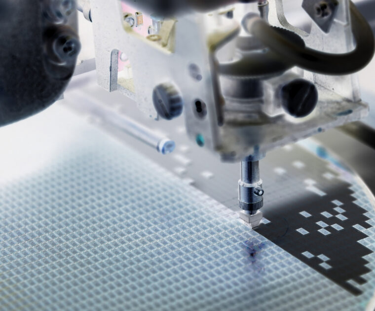
Working with a world-class high-volume foundry makes scaling up from low to high volume as…
Working with a world-class high-volume foundry makes scaling up from low to high volume as easy as putting a purchase order in place. Instead of having to buy equipment, develop processes, and train operators over many years, a fabless photonics developer can leverage foundries who already have these capabilities and knowledge.
Thanks to wafer scale technology, electronics has successfully driven down cost per transistor for many decades. This allowed the world to enjoy chips that every generation became smaller and provided exponentially more computing power for the same amount of money. This scale-up process is how everyone now has a computer processor in their pocket that is millions of times more powerful than the most advanced computers of the 1960s that landed men on the moon.
This progress in electronics integration is a key factor that brought down the size and cost of coherent transceivers, packing more bits than ever into smaller areas. However, photonics has struggled to keep up with electronics, and now the optics dominate the optical transceiver’s cost. If the transceiver cost curve does not continue to decrease, it will be difficult to achieve the goal of making coherent technology more accessible across the entire optical network. This will make it more difficult to provide the services needed by cloud providers and the growing 5G access networks.
As we mentioned in our previous article, photonics manufacturing must move into wafer-scale territory to provide faster, more affordable, and sustainable coherent transmission.
However, most photonic chip developers don’t have human and financial resources to own and operate their own wafer-scale photonic foundries. Fortunately, electronic chip developers have shown a more viable and cost-effective alternative: the fabless model.
Increasing the volume of photonics manufacturing is a big challenge. Some photonic chip developers choose to manufacture their chips in-house within their own fabrication facilities. This approach has some strong advantages, as it gives component manufacturers full control over their production process. By vertically integrating the whole chip design, manufacturing, and testing process within the same company, it’s often easier to try out new changes and innovations to the product.
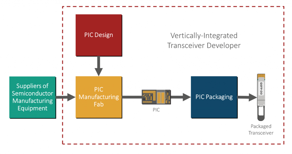
However, this approach has its trade-offs. If a vertically-integrated chip developer wants to scale up in volume, they must make a hefty investment in more equipment and personnel to do so. They must develop new fabrication process which not only need money, but also time to develop and train personnel. Especially in the case of an optical transceiver market that is not as big as that of consumer electronics, it’s hard not to wonder whether that initial investment is cost-effective.
Electronics manufacturing had a similar problem during their 1970s boom, with smaller chip start-ups facing almost insurmountable barriers to enter the market because of the massive capital expenditure (CapEx) required. Electronics solved this problem by moving into what we call a fabless model, with companies designing and selling the chips but outsourcing the manufacturing.
For example, transceiver DSP chip developers design the chip, but then outsource the actual fabrication to a large-volume manufacturing plant (usually called a foundry). This business model works by leveraging the design, research, development, and distribution networks of the fabless company, and the specialized manufacturing skill of the chip foundry.
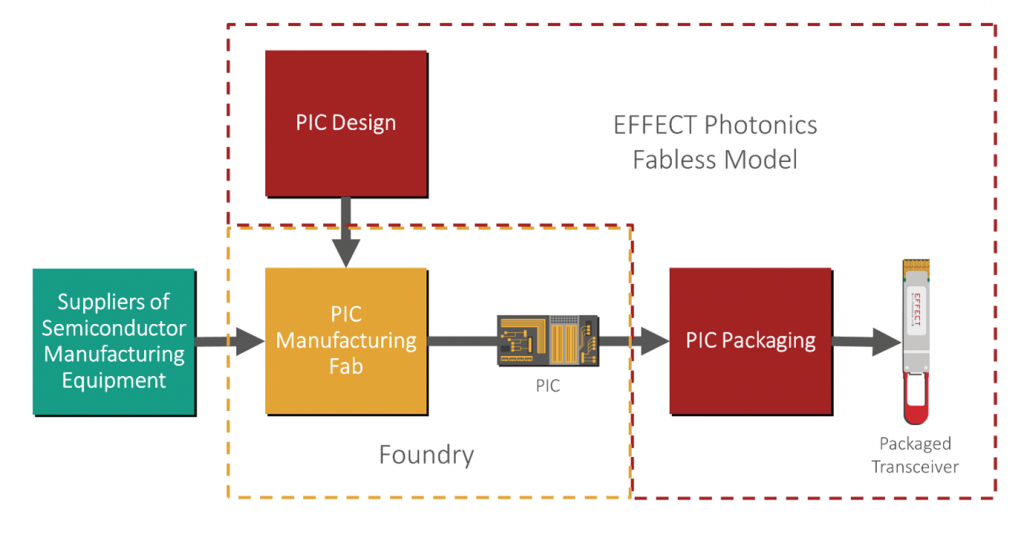
This model reduces the capital expenditure burden on the DSP developers, because instead of spending all the time and energy in scaling up their own facilities, they can work with a foundry that already did that investment and has the required manufacturing volume. In other words, instead going through a more costly, time-consuming process, the troubles of scaling up are outsourced and (from the perspective of the fabless company) become as simple as putting a purchase order in place. Furthermore, the fabless model also allows companies to concentrate their R&D resources on the end market. If photonics is to move into million-scale volumes, this is likely the way forward.
Even if an optical transceiver developer could move forward with the CapEx required for its own large-scale fab and a vertically-integrated model, market demand and operational expenses become the next pain point. Transceivers are a B2B market, and their demand is significantly smaller than of B2C consumer electronics. For example, LightCounting estimates that 55 million optical transceivers will be sold in 2021, while the International Data Corporation estimates that 1.4 billion smartphones will be sold in 2021. The latter figure is 25 times larger than that of the transceiver market.
The smaller demand of transceivers means that even if a vertically-integrated transceiver developer upgrades to a larger-scale manufacturing facility, it will likely have more manufacturing capacity than what their customers need. In such a situation, the facility could run at a reduced capacity. However, fabs are not only expensive to build, but also to operate. Unless they can be kept at nearly full utilization, operating expenses (OpEx) will become a drain on the finances of the facility owners.
This issue was something the electronics industry faced in the past, during the 1980s. Integrated electronics manufacturers had excess production capacity, and this situation paved the way for the fabless model too. The large-scale manufacturers ended up selling that excess capacity to smaller, fabless chip developers. Ultimately, the entire electronics industry relied increasingly on the fabless model, to the point where pure play foundries like the Taiwan Semiconductor Manufacturing Corporation (TSMC) appeared and focused entirely on manufacturing for other fabless companies.
In this scenario, everyone ended up winning. The foundries serviced multiple companies and could run their facilities at full capacity, while the fabless companies could outsource manufacturing and reduce their expenditures.
The other advantage of pure play foundries is that they not only have state-of-the art equipment but also the best personnel and technical expertise. Even if a vertically-integrated developer transceiver can make the required CapEx to scale up their facilities, developing processes and training people inevitably takes years, delaying the return on investment even further.
By working with an established and experienced foundry, fabless companies take advantage of the highly trained and experience personnel of these facilities. These operators, technicians, and engineers have worked day in, day out with their equipment for years and already developed processes that are finely tuned to their equipment. Thanks to their work, fabless transceiver developers do not have to reinvent the wheel and come up with their own processes, saving valuable time and many, many headaches.
To make transceivers more accessible to world and connect more people together, transceiver developers need to reach production scales in the millions. At EFFECT Photonics, we believe that the way to achieve this goal is by having photonics follow the blueprint laid out by the electronics industry. Using a fabless model, we can reduce the capital expenditure and scale up more quickly and with fewer risks.
Working with a world-class high-volume foundry makes scaling up from low to high volume as easy as putting a purchase order in place. Instead of having to buy equipment, develop processes, and train operators over many years, a fabless photonics developer can leverage foundries who already have these capabilities and knowledge.
Tags: coherent, coherent optics, external foundries, foundries, Integrated Photonics, LightCounting, optical transceivers, photonic integration, Photonics, photonicwafer, pluggables, Transceivers, wafer
Coherent transmission has become a fundamental component of optical networks to address situations where direct…
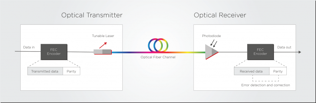
Coherent transmission has become a fundamental component of optical networks to address situations where direct detect technology cannot provide the required capacity and reach.
While direct detect transmission only uses the amplitude of the light signal, coherent optical transmission manipulates three different light properties: amplitude, phase, and polarization. These additional degrees of modulation allow for faster optical signals without compromising the transmission distance. Furthermore, coherent technology enables capacity upgrades without replacing the expensive physical fiber infrastructure on the ground.
The digital signal processor (DSP) is the electronic heart of coherent transmission systems. The fundamental function of the DSP is encoding the electronic digital data into the amplitude, phase, and polarization of the light signal and decoding said data when the signal is received. The DSP does much more than that, though: it compensates for impairments in the fiber, performs analog-to-digital conversions (and vice versa), corrects errors, encrypts data, and monitors performance. And recently, DSPs are taking on more advanced functions such as probabilistic constellation shaping or dynamic bandwidth allocation, which enable improved reach and performance.
Given its vital role in coherent optical transmission, we at EFFECT Photonics want to provide an explainer of what goes on inside the DSP chip of our optical transceivers.
Even though we colloquially call the chip a “DSP”, it is an electronic engine that performs much more than just signal processing. Some of the different functions of this electronic engine (diagram below) are:
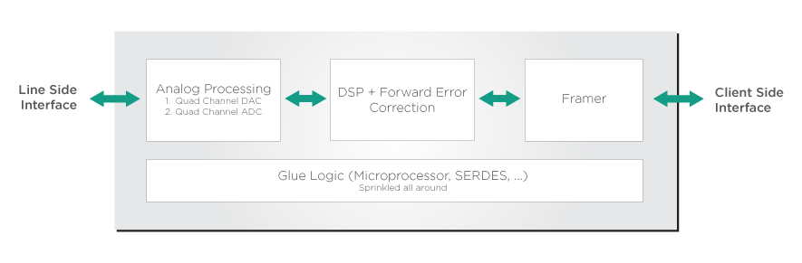
We must highlight that each of these blocks has its own specialized circuitry and algorithms, so each is a separate piece of intellectual property. Therefore, developing the entire electronic engine requires ownership or access to each of these intellectual properties.
Having clarified first all the different parts of a transceiver’s electronic engine, we can now talk more specifically about the actual DSP block that encodes/decodes the data and compensates for distortions and impairments in the optical fiber. We will describe some of the critical functions of the DSP in the order in which they happen during signal transmission. Receiving the signal would require these functions to occur in the opposite order, as shown in the diagram below.
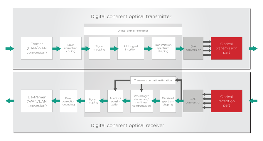
When transmitting, the signal goes through the digital-to-analog conversion after this whole DSP sequence. When receiving the signal, it goes through the inverse analog-to-digital conversation and then through the DSP sequence.
This is an oversimplification, but we can broadly classify the two critical areas of improvement for DSPs into two categories.
The entire field of communication technology can arguably be summarized with a single question: how can we transmit more information into a single frequency-limited signal over the longest possible distance?
DSP developers have many tools in their kit to answer this question. For example, they can transmit more data using more states in their quadrature-amplitude modulation process. The simplest kind of QAM (4-QAM) uses four different states (usually called constellation points), combining two different intensity levels and two different phases of light.
By using more intensity levels and phases, more bits can be transmitted in one go. State-of-the-art commercially available 400ZR transceivers typically use 16-QAM, with sixteen different constellation points that arise from combining four different intensity levels and four phases. However, this increased transmission capacity comes at a price: a signal with more modulation orders is more susceptible to noise and distortions. That’s why these transceivers can transmit 400Gbps over 100km but not over 1000km.
One of the most remarkable recent advances in DSPs to increase the reach of light signals is probabilistic constellation shaping (PCS). In the typical 16-QAM modulation used in coherent transceivers, each constellation point has the same probability of being used. This is inefficient since the outer constellation points that require more power have the same probability as the inner constellation points that require lower power.
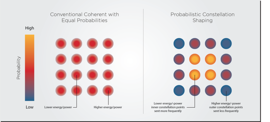
PCS uses the low-power inner constellation points more frequently, and the outer constellation points less frequently, as shown in Figure 5. This feature provides many benefits, including improved tolerance to distortions and easier system optimization to specific bit transmission requirements. If you want to know more about it, please read the explainers here and here.
Increases in transmission reach and efficiency must be balanced with power consumption and thermal management. Energy efficiency is the biggest obstacle in the roadmap to scale high-speed coherent transceivers into Terabit speeds.
Over the last two decades, power ratings for pluggable modules have increased as we moved from direct detection to more power-hungry coherent transmission: from 2W for SFP modules to 3.5 W for QSFP modules and now to 14W for QSSFP-DD and 21.1W for OSFP form factors. Rockley Photonics researchers estimate that a future electronic switch filled with 800G modules would draw around 1 kW of power just for the optical modules.
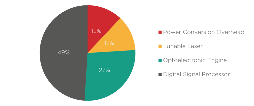
Around 50% of a coherent transceiver’s power consumption goes into the DSP chip. Scaling to higher bandwidths leads to even more losses and energy consumption from the DSP chip, and its radiofrequency (RF) interconnects with the optical engine. DSP chips must therefore be adaptable and smart, using the least amount of energy to encode/decode information. You can learn more about this subject in one of our previous articles. The interconnects with the optical engine are another area that can see further optimization, and we discuss these improvements in our article about optoelectronic co-design.
In summary, DSPs are the heart of coherent communication systems. They not only encode/decode data into the three properties of a light signal (amplitude, phase, polarization) but also handle error correction, analog-digital conversation, Ethernet framing, and compensation of dispersion and nonlinear distortion. And with every passing generation, they are assigned more advanced functions such as probabilistic constellation shaping.
There are still many challenges ahead to improve DSPs and make them transmit even more bits in more energy-efficient ways. Now that EFFECT Photonics has incorporated talent and intellectual property from Viasat’s Coherent DSP team, we hope to contribute to this ongoing research and development and make transceivers faster and more sustainable than ever.
Tags: 100G, 5G, 6G, access, access networks, aggregation, backhaul, capacity, coherent, DWDM, fronthaul, Integrated Photonics, live events, metro, midhaul, mobile, mobile access, mobile networks, network, optical networking, optical technology, photonic integrated chip, photonic integration, Photonics, PIC, PON, programmable photonic system-on-chip, solutions, technology, VR, WDM
Cable networks, just like any other telecom network in the world, had to adapt to…
Cable networks, just like any other telecom network in the world, had to adapt to the rising demand for data. During the 90s and 00s, these requirements led to the rise of hybrid fiber-coaxial (HFC) networks: optical fibers travel from the cable company hub and terminate into optical nodes, while coaxial cable connects the last few hundreds of meters from the optical node to nearby houses. These connections mainly were asymmetric, with customers having several times more bandwidth to download data than to upload.
In the past decade, the way we use the Internet has changed. With the rise of social media, online gaming, video calls, and independent content creation such as video blogging, users need more upstream bandwidth than ever. These new requirements have led to quick progress in the DOCSIS standards that regulate data transmission over coaxial cables. For example, the latest DOCSIS 4.0 standards allow full-duplex transmission with symmetrical upstream and downstream channels. Meanwhile, fiber-to-the-home (FTTH) systems—with fiber arriving directly to the customer premises—are also becoming widespread and allowing Gigabit connections that are faster than HFC networks.
Despite these upgrades in the transport mediums and standards, cable networks have experienced surprisingly few upgrades in their architectures. They still rely on centralized architectures in which the network operator’s headend performs almost all functionalities of both the physical layer (PHY) and medium access control layer (MAC). This means that the headend must modulate and demodulate data, convert between analog and digital, perform error corrections, provide cable modem termination system (CMTS) services, and do some resource allocation and flow control.
However, as traffic demands grow, cable providers need to deliver more and more bandwidth to their optical nodes and customer premises. The headend equipment is getting more congested, consuming more power, and running out of ports to handle more fiber connections. This solution centralized on the headend is struggling to scale up with increased demand. As it often happens in the telecom sector, operators need to figure out ways to deliver more bandwidth to more customers without spending significantly more money.
These issues are the reason why cable providers are moving into distributed access architectures (DAA) that can spread functionalities across access network nodes and reduce the port congestion and equipment required at the headend. Remote PHY has become increasingly popular among providers because it separates the PHY layer from the traditional cable headend and pushes its functions (such as modulation or digital-analog conversion) into the optical fiber access nodes of the network.
This shift can enhance the performance, capacity, and reliability of fixed access networks by using more digital transmission. It also reduces the complexity and power consumption of the headend, which previously translated into higher costs due to the required cooling.
Furthermore, separating PHY and MAC layers makes it easier to virtualize headends and their network functions, which significantly cuts expenses due to the use of commercial-off-the-shelf (COTS) equipment compared to more specialized equipment. Virtualization also allows deploying new services and applications more quickly to users and migrating workloads to optimize power consumption and reduce energy costs. On top of that, Remote PHY achieves all of these benefits while keeping the existing HFC infrastructure!
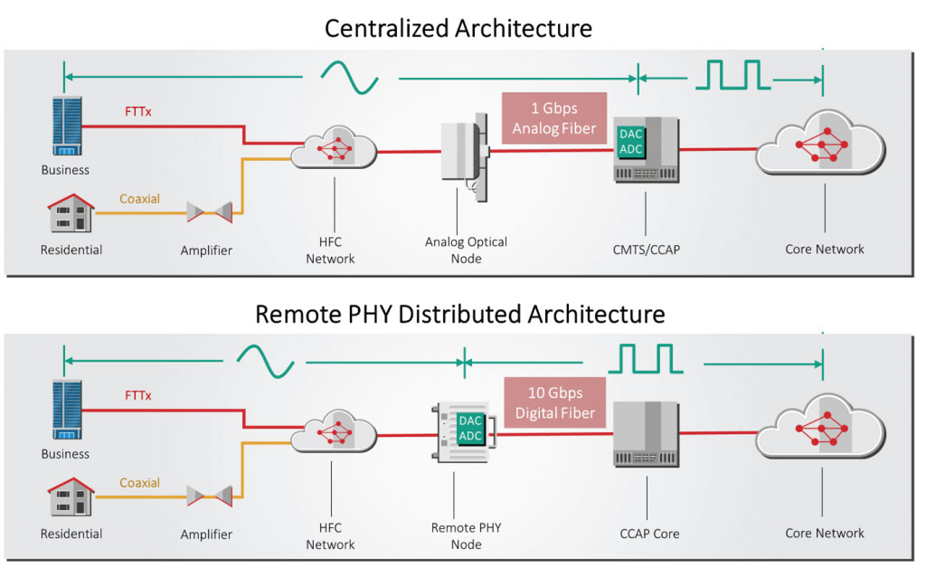
One of the most significant upgrades provided by Remote PHY networks is digital transmission deeper into the access network. In Remote PHY, data and video signals are kept in a digital format beyond the core headend, all the way into the upgraded optical node, where the signal is then converted into analog RF format. The fiber links between the headend and the access node that were previously analog will become digital fiber connections over Ethernet.
Since digital signals are more noise-tolerant than analog signals, the network benefits from this increased digital transmission length. Analog and radiofrequency signals now travel smaller distances to reach customer premises, so the signal accumulates less noise and boosts its signal-to-noise ratio. This improvement potentially allows the delivery of higher bandwidth signals to customers, including an increase in upstream bandwidth. Furthermore, the reliability of the link between the headend and the new optical node increases due to the greater robustness of digital links. These advances in reliability and performance make digital optics more affordable to buy and maintain than analog optics, reducing the costs for the network operators.
Let’s provide a very simplified example of how it all comes together. A network operator wants to increase their bandwidth and serve more customers, but their traditional centralized headend is already crowded with eight analog optical fiber links of 1Gbps each. There is no room to upgrade.
By installing Remote PHY technology in both the headend and the node, those analog links can be replaced by higher-capacity 10G digital links. The increased capacity at the headend allows for more optical node splits, while the new digital-to-analog conversion capability of the nodes allows them to care of more coaxial splits, all to serve new areas and customers.
The tremendous progress in electronic and photonic integration made Dense Wavelength Division Multiplex (DWDM) technology affordable and available to access networks, and this technology is quickly becoming a workhorse in this network domain. The availability of affordable DWDM transceivers made the deployment of Remote PHY even more powerful.
With Remote PHY improving the capacity of the headend, cable access networks had more bandwidth to serve more customers. However, some ways of using that bandwidth are more efficient than others. Operators can do extra node splits for customers by using their dark fibers and more grey transceivers, but that solution doesn’t scale in so cost-effectively due to the installation and maintenance of a new fiber link. Another option is time division multiplexing (TDM), which multiplexes the data of different node channels into specific time slots. This solution allows operators to carry different node channels in a single fiber but has speed, latency, and security trade-offs. A single time-multiplexed channel cannot transmit at the same speed and latency as a dedicated channel, and the data of all node channels are in the same multiplexed optical link, so the nodes and their customers can’t have fully secure channels to themselves.
DWDM solutions, on the other hand, can avoid the speed and security trade-offs by multiplexing extra channels into different wavelengths of light. Instead of several TDM channels “splitting” the 10G bandwidth among themselves, the DWDM channels can each transmit at 10G. And since each WDM channel has its own wavelength, the channels are transmitted independently from each other, allowing users to have secure channels.
Without sharing an optical link as in TDM, DWDM channels can also provide bidirectional communication (upstream and downstream) with less electronic processing than TDM channels. This feature is particularly beneficial for the modern Internet consumption patterns described earlier in the article.
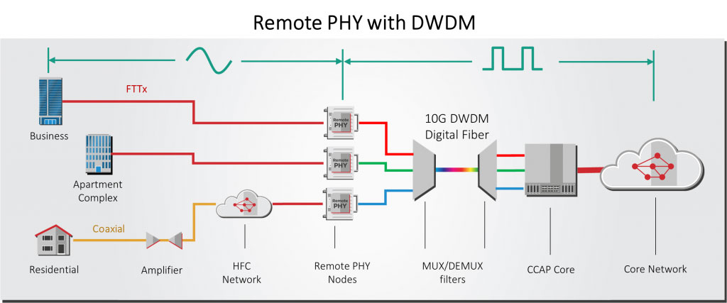
Let’s go back to our previous example of the upgraded headend with 10G digital fiber links. Thanks to DWDM technology, a single 10G port on this headend can support additional optical nodes in the network more cost-effectively than ever. Let’s say a new apartment complex was built, and the network operator needs to deploy a new node to service this new building. In the past, this deployment would have required lighting up a dark fiber and setting up an extra fiber link or using TDM technology with lower data rates, latency, and security. With DWDM, the new node can simply be carried through a different wavelength channel in the already existing fiber link. And as we will describe in our next article, autotuneability in DWDM transceivers makes their setup and maintenance even more affordable.
Cable networks need to serve more customers than ever with more symmetric upstream and downstream capacity, and they need to achieve this without changing their existing fiber and coaxial infrastructure. These goals become possible with the onset of Remote PHY and more accessible DWDM transceivers. By separating the MAC and PHY layer, Remote PHY reduces the load on the cable headend and allows for more virtualization of network functions, making it easier and more affordable to upgrade and manage the network. Meanwhile, DWDM enables connections from the headend to the Remote PHY nodes that serve tens of customers with a single fiber.
Tags: architectuyre, autotuneability, DWDM, fixed access networks, Integrated Photonics, optical transceivers, photonic integration, Photonics, pluggables, remote phy, Transceivers, tuneability
The increasing use of data and fiercely price-conscious and multimedia-hungry business subscribers can limit revenue…
The increasing use of data and fiercely price-conscious and multimedia-hungry business subscribers can limit revenue opportunities for the network provider industry. Providers must therefore look elsewhere to grow their customer base, open new revenue streams, and boost margins. So how can they adapt their business strategies and achieve growth objectives?
Just as operators scale up high-capacity data center interconnects to cope with these needs, providers can add Ethernet services for high-capacity services. These can offer a differentiated and competitive service to corporate customers, ranging from 1G to 100G and beyond. Not only will Ethernet services add a cost-effective alternative to existing services, but they also ensure business Ethernet offerings are set up to complement wide area networks and hybrid network services.
According to Ovum, the global enterprise Ethernet services market will grow at 10.7% CAGR, exceeding $70bn by 2020 (Ovum’s Ethernet Services Forecast, Sep 2015), and is now the de facto wide-area network data connectivity technology. Ethernet will be a significant portion of the data service market driven by enthusiasm for higher bandwidth services. This growth will continue as we adopt more cloud-based applications and enterprises embrace digital transformation. Business Ethernet solutions can be further boosted with tunable DWDM transceivers.
With applications and data volumes exploding in organizations of all types and sizes, there is an increasing need for 1GbE+ connections, with 10GbE+ connectivity for company headquarters and even 100GbE+ connections for data center connectivity. Specifically, demand is being driven by the proliferation of bandwidth-hungry applications. An MRI scan, for example, can be a 300GB file, which would take around 7 hours to download over a 100Mbps connection. Over a 10GbE link, that time falls to just 4 minutes and 28 seconds on a 100GbE link – this can be the difference between life and death when a consultant needs to make a time-critical decision on how to treat their patient best.
Enterprises know all about cost-containment and budget constraints. Virtual private networks (VPNs) based on legacy MPLS protocols have their place when delivering wide-area connectivity. These VPNs can offer any-to-any connectivity and scale to thousands of sites – but, at the higher speeds needed for high-bandwidth applications, they can be significantly more expensive than business Ethernet to deploy and maintain.
In addition, the MPLS routers needed for IP VPN have acquired more and more protocols and complexity over the last few decades. The cost of implementing all of these protocols, and securing them against attack, has driven leading service providers to demand a radically more straightforward way of building networks.
With business Ethernet, the network infrastructure and management can be unified under Ethernet protocol, making the network easier to plan, deploy and manage at scale. This means fewer routers, more remotely programmable services, and fewer truck rolls resulting in a lower cost per bit than comparable VPN solutions. These savings scale across 1GbE, 10GbE, and 100GbE connections with less CAPEX investment, helping to increase the predictability of delivery costs over time. WDM solutions can further boost this capacity.
Almost every organization uses the cloud in some capacity, whether for development and test resources or software-as-a-service applications. While the cost and flexibility of the cloud are compelling, many IT executives overlook the importance of fast, high-bandwidth wide-area connectivity to make cloud-based applications work as they should.
These needs might require businesses with huge traffic loads to upgrade to 25G, 100G, or even 400G speeds. These capacity needs would require coherent technology. Fortunately, advances in electronic and photonic integration have miniaturized coherent line card transponders into pluggable modules the size of a large USB stick.
Many of these business applications will require links between 25 Gbps and 100 Gbps that span several tens of kilometers to connect to the network provider’s headend. For these sites, the 400ZR pluggables that have become mainstream in datacom applications are not cost-effective when utilization is so low. This is where 100ZR technology comes into play.
100ZR is currently a marketing term for a short-reach (~80 km) coherent 100Gbps in a QSFP pluggable. Targeted at the metro edge and enterprise applications that do not require 400Gbps, 100ZR provides a lower-cost, lower-power pluggable that also benefits from compatibility with the large installed base of 50 GHz and legacy 100 GHz DWDM/ROADM line systems.
Businesses that need to aggregate many sites and branches into their networks will likely require tunable transceiver solutions to interconnect them. The number of available channels in tunable modules can quickly become overwhelming for technicians in the field. There will be more records to examine, more programming for tuning equipment, more trucks to load with tuning equipment, and more verifications to do in the field. These tasks can take a couple of hours just for a single node. If there are hundreds of nodes to install or repair, the required hours of labor will quickly rack up into the thousands and the associated costs into hundreds of thousands. Self-tuning modules significantly overcome these issues and make network deployment and maintenance more straightforward and affordable.
Self-tuning allows technicians to treat DWDM tunable modules the same way they would grey transceivers. There is no need for additional training for technicians to install the tunable module. There is no need to program tuning equipment. There is no need to obsessively check the wavelength records and tables to avoid deployment errors on the field. Technicians only need to follow the typical cleaning and handling procedures, plug the transceiver, and the device will automatically scan and find the correct wavelength once plugged. This feature can save providers thousands of person-hours in their network installation and maintenance and reduce the probability of human errors, effectively reducing capital and operational expenditures (OPEX).
With business Ethernet, one can set up super-fast connections for customers and connect their locations and end-users with any cloud-based services they use. Business Ethernet solutions can be further boosted with tunable DWDM transceivers. If business future-proof their networks with upgrades like 100ZR transceivers, they can scale up connectivity seamlessly to ensure that applications always provide an excellent end-user experience. That connectivity is never a limiting factor for customers’ cloud strategies. As the business sector seeks to upgrade to greater capacity and easier management, tunable and coherent transceivers will be vital in addressing their needs.
Tags: 5G, access, aggregation, backhaul, capacity, DWDM, fronthaul, Integrated Photonics, LightCounting, metro, midhaul, mobile, mobile access, network, optical networking, optical technology, photonic integrated chip, photonic integration, PIC, PON, programmable photonic system-on-chip, solutions, technology© 2026 EFFECT PHOTONICS All rights reserved. T&C of Website - T&C of Purchase - Privacy Policy - Cookie Policy - Supplier Code of Conduct