– Link Magazine

⚠️ Website Under Construction
– Link Magazine

Eindhoven, The Netherlands During King Willem-Alexander’s visit to the High Tech Campus in Eindhoven on…
During King Willem-Alexander’s visit to the High Tech Campus in Eindhoven on April 20, he gained insight into the value chain of integrated photonics in the Netherlands and Europe from various perspectives. This emerging chip technology is accelerating thanks to a €1.1 billion program led by PhotonDelta. With demonstrations at Holst Centre and roundtable discussions at PhotonDelta, the King learned about the essence of the technology, its applications, and its importance for the future of the Netherlands and Europe.
Ewit Roos, CEO of PhotonDelta, is very pleased with the day’s outcome.
Ewit Roos, CEO at PhotonDeltaThe King’s visit is a tremendous honor for the ecosystem. It underlines once again the importance of integrated photonics for our country. We told him about the applications of integrated photonics for innovations in medical diagnostics, autonomous driving, the agricultural sector, and data communications. PhotonDelta and Holst Centre are central to the development of this new value chain. For the King, this was certainly a wonderful opportunity to get the most complete picture possible of the quality of the unique position of the ecosystem and all the opportunities that still lie ahead.
Photonics is all about the interaction between light (photons) and matter. Through photonics, data can be transmitted at the speed of light, reducing energy consumption and increasing efficiency. Integrated photonic chips, considered a key technology worldwide, enable the development of smaller, faster, and energy-efficient devices. This will lead to innovations that will help solve the major challenges of our time and contribute to a healthy and sustainable future.
The Netherlands has recognized the opportunities of integrated photonics through the National Growth Fund. PhotonDelta, the ecosystem of organizations in photonic chip technology, has mobilized public and private investment totaling 1.1 billion euros through this fund to transform the Netherlands into a leader in the next generation of semiconductors.
The investment consists of 470 million euros through the growth fund, with the rest coming from other partners and stakeholders. It is all part of the Dutch government’s plan to strengthen the country’s position as a world leader in integrated photonics.
The King first visited Holst Centre, a collaboration between the research centers imec and TNO. Researchers from different disciplines develop new technology for photonic chips and prototypes that companies can use for their production process and new products.
The King was given a tour of Holst Centre’s laboratory and attended demonstrations of the application of photonics in various sectors. Representatives from Signify, EFFECT Photonics, Delta Diagnostics, Quix Quantum, and Lionix explained the different stages in the value chain. During this tour, the main focus was on the applications that help solve society’s critical challenges.
Integrated photonics is one of the pillars of Holst Centre’s strategy. By combining the expertise of imec and TNO, many aspects needed in the development and production process can be offered, such as design, prototyping, testing, and manufacturing. We combine the photonic microchip technology of imec in Belgium, the complementary photonic platforms in the Netherlands, the design expertise of imec in the Netherlands, and the optics and systems integration knowledge of TNO to help develop new sustainable solutions in different industries.
Kathleen Philips, director of imec at Holst Centre
The subsequent visit to PhotonDelta, also at the High Tech Campus, began with a presentation on the ecosystem. In recent years, PhotonDelta has grown this community from 12 to 60 stakeholders who together form a value chain that conceives, develops, and makes photonic chips and solutions based on them. The roundtable discussion covered topics such as industrialization, application technology, and European cooperation. Phix Photonics Assembly, Smart Photonics, and Trumpf Photonics Components addressed the challenges and possible solutions in scaling up the most crucial industrialization processes. Following this talk, Synopsys NL and NXP discussed the challenges around application strategies: creating a library of easy-to-use building blocks for new applications. Finally, the European playing field came into focus through PhotonDelta itself and the Ministry of Economic Affairs. This covered Europe’s ambitions around strategic autonomy and the impact of the European Chips Act. Photonic chips have been designated as a key technology by the European Commission. Security of supply for digital technology is the guiding principle in the Chips Act.
Strategic autonomy does not mean developing a copy of the global semiconductor value chain in Europe, but taking unique European positions in these chains where we can be ‘world-class’. This implies interdependence through quality and capacity rather than taking over one-to-one what is already happening elsewhere. Integrated photonics is one such position where Europe can excel.
Ton van Mol, Director TNO at Holst Centre
PhotonDelta is an ecosystem of organizations that conceive, develop and make solutions based on photonic chips. PhotonDelta supports the system by stimulating collaboration between stakeholders, providing funding, and connecting them to the market.
Holst Centre, a collaboration of imec and TNO, brings together expertise in wireless sensor technologies and flexible electronics under one roof. The sharing of specific knowledge in an open structure enables the alignment of research and innovation with societal issues in health and vitality, energy and climate, and mobility and industry 5.0.
# # #
More information:
PhotonDelta
Jorn Smeets, Chief Marketing Officer
M: 06 – 1147 8812
E: jorn@photondelta.com
W: www.photondelta.com
Imec at Holst Centre
Carolien van der Leegte, Communicatiemanager imec NL
M: 06 – 1760 4841
E: carolien.vanderleegte@imec.nl
W: www.holstcentre.com
W: www.imec-int.com
TNO at Holst Centre
Sara Joosten, Project Manager Marketing & Communications
M: 06 – 2915 6716
E: sara.joosten@tno.nl
W: www.holstcentre.com
W: www.tno.nl
EFFECT Photonics is a corporate member of the European Photonics Industry Consortium (EPIC), the industry…
EFFECT Photonics is a corporate member of the European Photonics Industry Consortium (EPIC), the industry association that promotes the sustainable development of organizations working in the field of photonics in Europe. EPIC fosters a vibrant photonics ecosystem by maintaining a strong network and acting as a catalyst and facilitator for technological and commercial advancement. EPIC publishes market and technology reports, organizes technical workshops and B2B roundtables, supports EU funding proposals, advocacy and lobbying, education and training activities, standards and roadmaps, pavilions at exhibitions. www.epic-assoc.com
Together with other members from the photonics related technologies, we at EFFECT Photonics are committed to actively contribute to the technological and commercial advancement of the integrated photonics industry globally. EFFECT Photonics delivers highly integrated optical communications products based on its Dense Wavelength Division Multiplexing (DWDM) optical System-on-Chip technology. The key enabling technology for DWDM systems is full monolithic integration of all photonic components within a single chip and being able to produce these in volume with high yield at low cost. With this capability, EFFECT Photonics is addressing the need for low cost DWDM solutions driven by the soaring demand for high bandwidth connections between datacenters and back from mobile cell towers. Headquartered in Eindhoven, The Netherlands, with additional R&D and manufacturing in South West UK, with sales partners worldwide. www.effectphotonics.com
This partnership is a significant addition to the already impressive member list of EPIC of more than 600 companies in 35 countries: https://www.epic-assoc.com/membership/epic-members/

Photonic integration will be a disruptive technology that will simplify network design and operation and…

The global optical transceiver market is expected to double in size by 2026, and coherent…
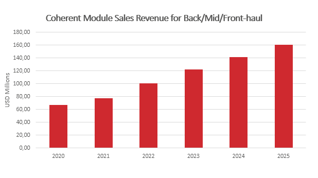
The global optical transceiver market is expected to double in size by 2026, and coherent pluggables will play a significant role in this growth as they will constitute roughly a third of those sales. While coherent is now an established solution in data center interconnects and long haul networks, it is also expected to start gaining ground in the access networks that connect mobile base stations and their controllers to the rest of the Internet. LightCounting forecasts that by 2025, coherent modules will generate 19% of all sales revenue, in an estimated market of $827 million, for transceivers in back-, mid-, and front-haul network segments. This is an increase in market share from 6% in 2021, as operators are expected to replace some of their direct detect modules with coherent ones in the coming years.
The numbers for coherent sales will only increase in the coming decade for two main reasons. First, electronic and photonic integration are making coherent pluggables economically viable and smaller (see one of our previous article on the subject). Second, the increasing data demands require access networks to increase their capacity beyond what direct detect can deliver. However, for coherent devices to become established in access networks, they must learn to live outdoors.
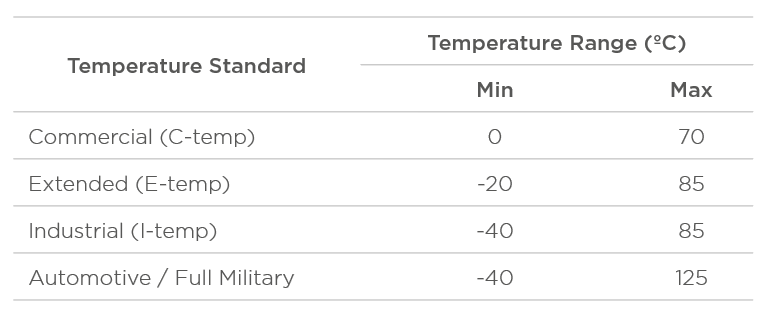
Coherent devices have traditionally lived in the controlled environments of data center machine rooms or network provider equipment rooms. These rooms have active temperature control, cooling systems, filters for dust and other particulates, airlocks, and humidity control. In these rooms, pluggable transceivers operate at a relatively stable temperature of around 50ºC, and they only need to survive in ambient temperatures within the commercial temperature range (C-temp) of 0 to 70ºC.
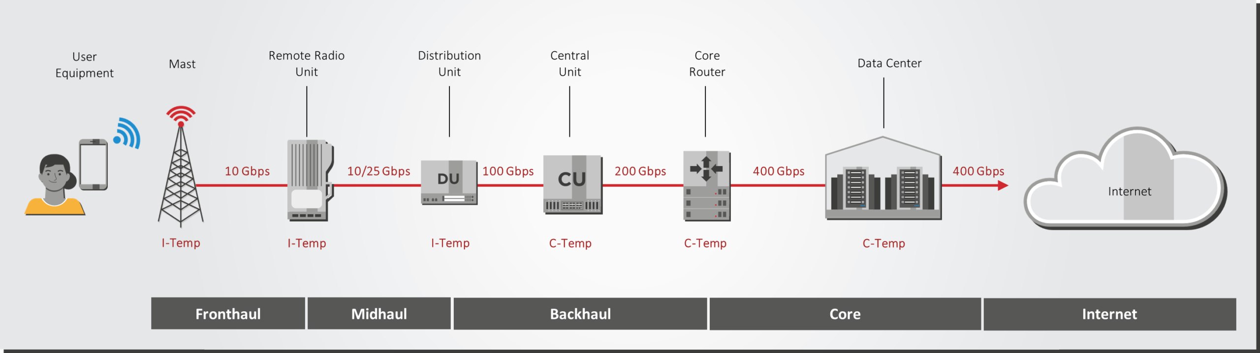
On the other hand, access networks feature uncontrolled outdoor environments at Mother Nature’s mercy and whims. It could be at the top of an antenna, on mountain ranges, inside traffic tunnels, or in the harsh winters of Northern Europe. Deployments at higher altitudes present additional problems. The air becomes less dense, so networking equipment cooling mechanisms don’t work as efficiently, so the device cannot tolerate case temperatures as high as it does at sea level. Transceivers should operate in the industrial temperature (I-temp) range of -40 to 85ºC degrees for these environments. Optics are also available in the extended temperature (e-temp) range, which can operate as hot as I-temp devices (85ºC) but cannot get any colder than -20ºC.
An expensive challenge for a network operator is having a product that cannot perform reliably in the uncontrolled environments of 5G deployments. With more bandwidth and computing power moving towards the network edges, coherent transceivers must endure potentially extreme conditions in outside environments. Since i-temp transceivers are more robust, they will survive for longer, and operators will ultimately buy fewer of them compared to c-temp modules. Therefore, the initial, somewhat more expensive investment in I-temp transceivers will pay off in the long run.
In addition, the growth of Internet-of-Things (IoT) applications makes reliability even more important. A network connection drop could be disastrous in many critical and business services, such as medical and self-driving car applications.
Making an I-temp transceiver means that every internal component—the integrated circuits, lasers, photodetectors—must also be I-temp compliant. EFFECT Photonics has already developed I-temp pluggable transceivers with direct detection, so we understand what standards must be followed to develop temperature-hardened coherent devices.
For example, our optical transceivers comply with the Telcordia GR-468 qualification, which describes how to test optoelectronic devices for reliability under extreme conditions. Our manufacturing facilities include capabilities for the temperature cycling and reliability testing needed to match Telcordia standards, such as temperature cycling ovens and chambers with humidity control.
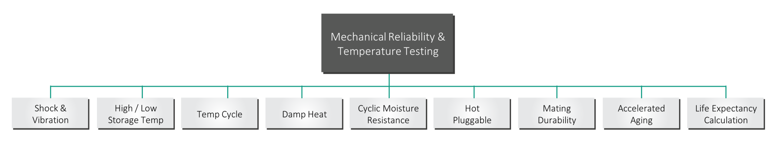
EFFECT Photonics transceivers also comply with the SFF-8472 standard that describes the Digital Diagnostics Monitoring (DDM) required for temperature-hardened transceivers to compensate for temperature fluctuations. Our proprietary NarroWave technology even allows network operators to read such device diagnostics remotely, avoiding additional truck rolls to check the devices on the field. These remote diagnostics give operators a full view of the entire network’s health from the central office.
One of our central company objectives is to bring the highest-performing optical technologies, such as coherent detection, all the way to the network edge. However, achieving this goal doesn’t just require us to focus on the optical or electronic side but also on meeting the mechanical and temperature reliability standards required to operate coherent devices outdoors. Fortunately, EFFECT Photonics can take advantage of its previous experience and knowledge in I-temp qualification for direct-detect devices as it prepares its new coherent product line.
If you would like to download this article as a PDF, then please click here.
Tags: access networks, coherent, coherent optics, commercial temperature, fiber networks, I-temp, industrial temperature, Integrated Photonics, LightCounting, NarroWave, network operators, optical transceivers, photonic integration, Photonics, pluggables, Transceivers
Direct Detection and Coherent: what is the difference between these technologies? What are their benefits…
Direct Detection and Coherent: what is the difference between these technologies? What are their benefits and limitations?
In the following video, we give a short explanation about these two technologies.
Firstly and foremost, Direct Detect and Coherent use different levels of information.
Direct Detection works by changing the amplitude of the light to transmit information. In this case, the achievable transmission distance depends on the speed of the data signal: at lower data rates, the transmission distance is more than 100 km, but as the speed increase, it exponentially gets shorter.
Coherent Optical Transmission uses three different properties of light: amplitude, phase, and polarization. This way, it is possible to increase the speed of the data signal, without compromising the transmission distance. With Coherent, it is possible to transmit information across long distances with very high data rates enabling operators to upgrade their networks without replacing the physical fiber infrastructure in the ground.
About EFFECT Photonics
EFFECT Photonics delivers highly integrated optical communications products based on its Dense Wavelength Division Multiplexing (DWDM) optical System-on-Chip technology. The key enabling technology for DWDM systems is full monolithic integration of all photonic components within a single chip and being able to produce these in volume with high yield at low cost. With this capability, EFFECT Photonics is addressing the need for low cost DWDM solutions driven by the soaring demand for high bandwidth connections between datacentres and back from mobile cell towers. EFFECT Photonics is headquartered in Eindhoven, The Netherlands, with additional R&D and manufacturing in South West UK, and a facility opening soon in the US.
http://www.effectphotonics.com
Tags: coherent, Coherent Detection, Direct Detect, Direct Detection, Integrated Photonics, Optical Coherent Technology, Optical Communication, optical networking, optical technology
Great achievement for EFFECT Photonics and TEGEMA!! On Monday, July 20, the 21 municipalities of…
Great achievement for EFFECT Photonics and TEGEMA!!
On Monday, July 20, the 21 municipalities of the Eindhoven Metropolitan Region (MRE) in the Netherlands awarded EFFECT Photonics and TEGEMA and for the important role both companies play in the development of integrated photonics. In the photo, Directors Pierre van Lamsweerde (Tegema) and Tim Koene (EFFECT Photonics) received the award of 50,000 euros from Jan Boersma of the municipality of Son and Breugel.
Full article in Dutch here: https://www.nu.nl/eindhoven/6065628/metropoolregio-overhandigt-twee-fotonicabedrijven-cheque-van-50000-euro.html
For more about our photonics technologies, visit: https://effectphotonics.com/technology/ultra-pure-light-sources/
Get in touch with us for further information by sending your request to: sales@effectphotonics.com

Before 2020, Apple made its computer processors with discrete components. In other words, electronic components…
Before 2020, Apple made its computer processors with discrete components. In other words, electronic components were manufactured on separate chips, and then these chips were assembled into a single package. However, the interconnections between the different chips produced losses and incompatibilities that made the device less efficient. After 2020, starting with Apple’s M1 processor, they now fully integrate all components on a single chip, avoiding losses and incompatibilities.
Apple’s fully integrated processor consumes a third of the power and lower costs than their older processors while still providing similar performance. EFFECT Photonics does something similar to what Apple did, but with optical components instead of electronic components. By integrating all the optical components (lasers, detectors, modulators, etc.) in a single system on a chip, we can minimize the losses and make the device more efficient. This approach is what we call photonic System-on-Chip (SoC).

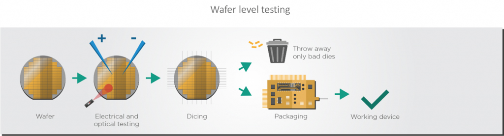
By integrating all optical components on a single chip, we also shift the complexity from the assembly process to the much more efficient and scalable semiconductor wafer process. Assembling and packaging a device by interconnecting multiple photonic chips increases assembly complexity and costs. On the other hand, combining and aligning optical components on a wafer at a high volume is much easier, which drives down the device’s cost. Testing is another aspect that becomes more efficient and scalable when manufacturing at the wafer level.
When faults are found earlier in the testing process, fewer resources and energy are spent processing defective chips. Ideally, testing should happen not only on the final, packaged transceiver but in the earlier stages of photonic SoC fabrication, such as measuring after wafer processing or cutting the wafer into smaller dies. Full photonic integration enables earlier optical testing on the semiconductor wafer and dies. By testing the dies and wafers directly before packaging, manufacturers need only discard the bad dies rather than the whole package, which saves time, and cost and is more energy-efficient and sustainable.

For example, EFFECT Photonics reaps these benefits in its production processes. 100% of electrical testing on the photonic SoCs happens at the wafer level, and our unique integration technology allows for 90% of optical testing on the wafer. The real-world applications of SoCs are practically limitless and priceless. Electronic SoCs are used in most, if not all, portable devices, such as smartphones, cameras, tablets, and other wireless technologies. SoCs are also frequently used in equipment involved in the Internet of Things, embedded systems, and, of course, photonics. Data center interconnects are an excellent example of an application that benefits from a photonic SoC approach. As DCIs demand higher performance and reach, it’s no longer sufficient to have a solution that integrates just some parts of a system.
That is why EFFECT Photonics’ business strategy aims to solve the interconnect challenges through a holistic photonic SoC approach that understands the interdependence of system elements. By combining the photonic SoC with highly optimized packaging with cost-effective electronics, we are building a high production volume platform that can meet the demands of the datacom sector.
Tags: DWDM, Integrated Photonics, network, optical networking, optical technology, photonic integrated chip, photonic integration, photonic system-on-chip, PIC, solutions, technology
EFFECT Photonics is pleased to announce the completion of its leadership team with the recent…
The advances in electronic and optical integration have brought down the size and cost of…
The advances in electronic and optical integration have brought down the size and cost of the coherent transceivers, packing more bits than ever into smaller areas. However, progress in the cost and bandwidth density of transceivers might slow down soon. Electronics has achieved amazing breakthroughs in the last two decades to continue increasing transistor densities and keeping Moore’s Law alive, but these achievements have come at a price. With each new generation of electronic processors, development costs increase and the price per transistor has stagnated.
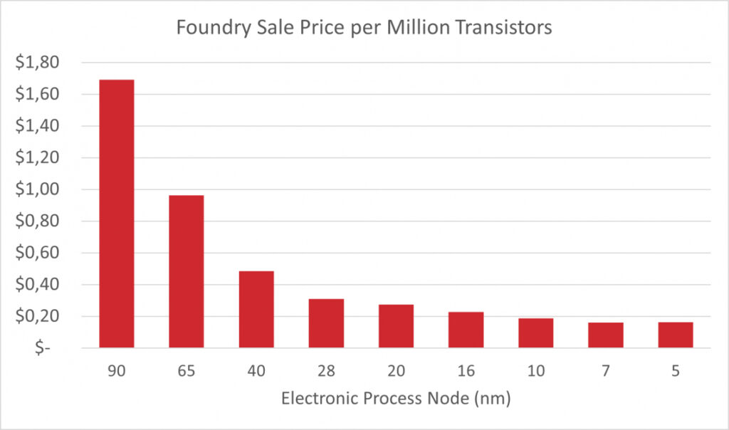
Due to these developments, electronic digital signal processor (DSP) chips will continue to improve in efficiency and footprint, but their price will stagnate and with it the price of optical transceivers. Without further improvements in the cost per bit, it will be difficult to achieve the goal of making coherent technology more accessible across the entire optical network. This will make it more difficult to provide the device volume and services needed by the growing 5G networks and cloud providers.
To make coherent transceivers more accessible, photonics has to step up now more than ever. With the cost of DSPs stagnating, photonic integration must take the lead in driving down the costs and size of optical transceivers. Integrating all optical components on a single chip makes it easier to scale up in volume, reach these size and cost targets, and ultimately provide faster, more affordable, and sustainable coherent transmission.
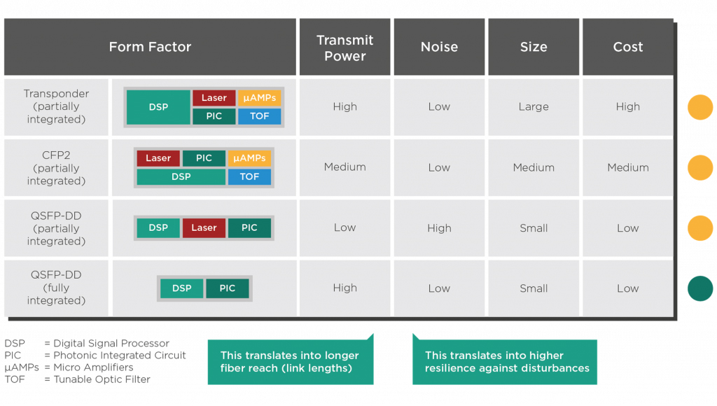
Full photonic integration allows us to combine active optical elements like the laser and the amplifer with passive elements, all on the same chip and enclosed in a simple, non-hermetic package. This process enables a much smaller device than combining several indivudally packaged elements. For example, by integrating all photonic functions on a single chip, including lasers and optical amplifiers, EFFECT Photonics’ pluggable transceiver modules can achieve transmit power levels similar to those of line card transponder modules while still keeping the smaller QSFP router pluggable form factor, power consumption, and cost.
Full integration technology increases the transmit power by minimizing the optical losses due to the use of more efficient optical modulators, fewer material losses compared to silicon, and the integration of the laser device on the same chip as the rest of the optical components. The semiconductor optical amplifiers (SOAs) used in fully integrated devices can also outperform the performance of micro-EDFAs for transmission distances of at least 80km.
As innovative as full photonic integration can be, it will have little impact if it cannot be manufactured at a high enough volume to satisfy the demands of mobile and cloud providers and drive down the cost per device. Wafer scale photonics manufacturing demands a higher upfront investment, but the resulting high-volume production line drives down the cost per device. This economy-of-scale principle is the same one behind electronics manufacturing, and the same must be applied to photonics.
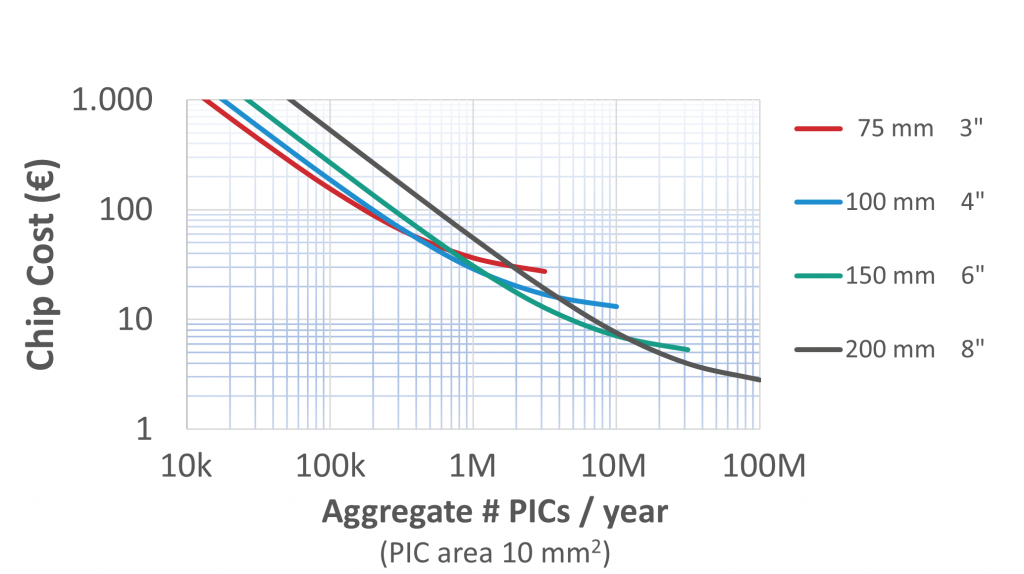
The more optical components we can integrate into a single chip, the more can the price of each component decrease. The more optical System-on-Chip (SoC) devices can go into a single wafer, the more can the price of each SoC decrease. Researchers at the Technical University of Eindhoven and the JePPIX consortium have done some modelling to show how this economy of scale principle would apply to photonics. If production volumes can increase from a few thousands of chips per year to a few millions, the price per optical chip can decrease from thousands of Euros to mere tens of Euros. This must be the goal for the optical transceiver industry.
Integrating all optical components on a single chip can make manufacturing and testing more efficient, sustainable, and easier to scale up. The price of photonic devices is not dominated by the manufacturing of the semiconductor chips, but by the device assembly and packaging. Assembling and packaging a device by interconnecting multiple photonic chips together leads to an increase in assembly complexity and therefore additional costs.
This situation happens frequently with the laser component, which is often manufactured on a separate chip and then interconnected to the other optical components which are on another chip. Integrating all components—including the laser—on a single chip shifts the complexity from the assembly process to the much more efficient and scalable semiconductor wafer process. For example, it’s much easier to combine optical components on a wafer at a high-volume than it is to align different chips together in the assembly process, and that drives down the cost of the device.
Testing is another aspect that becomes more efficient and scalable when manufacturing at the wafer level. When faults are found earlier in the testing process, fewer resources and energy are spent in process defective chips. Ideally, testing should happen not only on the final, packaged transceiver but in the earlier stages of PIC fabrication, such as measuring after wafer processing or cutting the wafer into smaller dies.
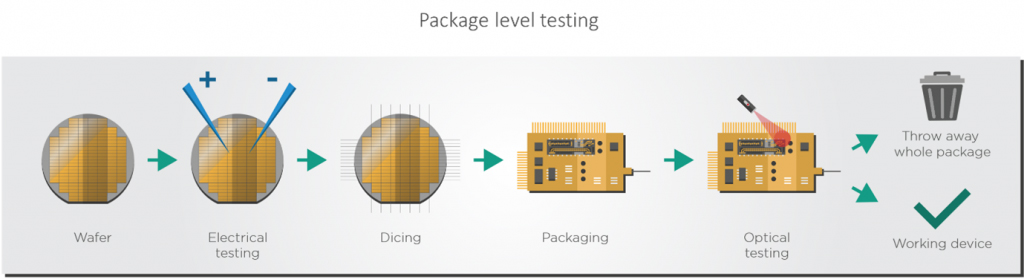
Full photonic integration enables earlier optical testing on the semiconductor wafer and dies. By testing the dies and wafers directly before packaging, manufacturers need only discard the bad dies rather than the whole package, which saves time, cost, and is more energy efficient and sustainable. For example, EFFECT Photonics reaps these benefits in its production processes. 100% of electrical testing on the PICs happens at the wafer level, and our unique integration technology allows for 90% of optical testing to also happen on the wafer.
Photonics is facing the next stage of its development. There have been many great breakthroughs that have allowed us to take photonic devices from the lab to real-world use cases. However, to have the biggest possible impact in society, we need to manufacture photonic devices at very high volumes to make them accessible to everyone. This requires us to think about production volumes in the scale of millions of units. At EFFECT Photonics, we believe that the way to achieve this goal is by following the blueprint laid out by our friends in the electronics industry. By integrating all optical components on a single chip, we can shift more complexity from the assembly to the wafer, allowing production to scale more efficiently and sustainably. In our next article, we will elaborate on another key factor of the electronics blueprint: the fabless development model.
Tags: coherent, coherent optics, Density, Integrated Photonics, LightCounting, network operators, optical transceivers, photonic integration, Photonics, pluggables, Transceivers, Wafer Scale Photonics© 2026 EFFECT PHOTONICS All rights reserved. T&C of Website - T&C of Purchase - Privacy Policy - Cookie Policy - Supplier Code of Conduct