– Link Magazine


– Link Magazine
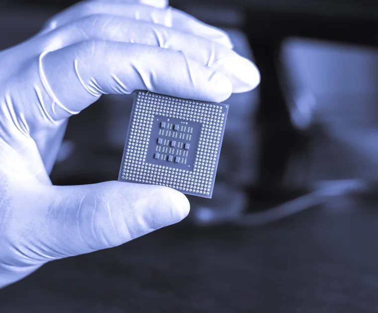
While packaging, assembly, and testing are only a small part of the cost of electronic…
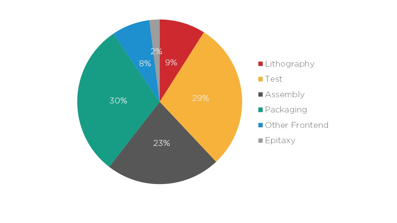
While packaging, assembly, and testing are only a small part of the cost of electronic systems, the reverse happens with photonic integrated circuits (PICs) and their subassemblies. Researchers at the Technical University of Eindhoven (TU/e) estimate that for most Indium Phosphide (InP) photonics devices, the cost of packaging, assembly, and testing can reach around 80% of the total module cost.
To trigger a revolution in the use of photonics worldwide, it needs to be as easy to manufacture and use as electronics. In the words of EFFECT Photonics’ Chief Technology Officer, Tim Koene: “We need to buy photonics from a catalog as we do with electronics, have datasheets that work consistently, be able to solder it to a board and integrate it easily with the rest of the product design flow.”
This article will explore three key avenues to improve optical subassemblies and packaging for photonic devices.
A key way to improve photonics manufacturing is to learn from electronics packaging, assembly, and testing methods that are already well-known and standardized. After all, building a new special production line is much more expensive than modifying an existing production flow.
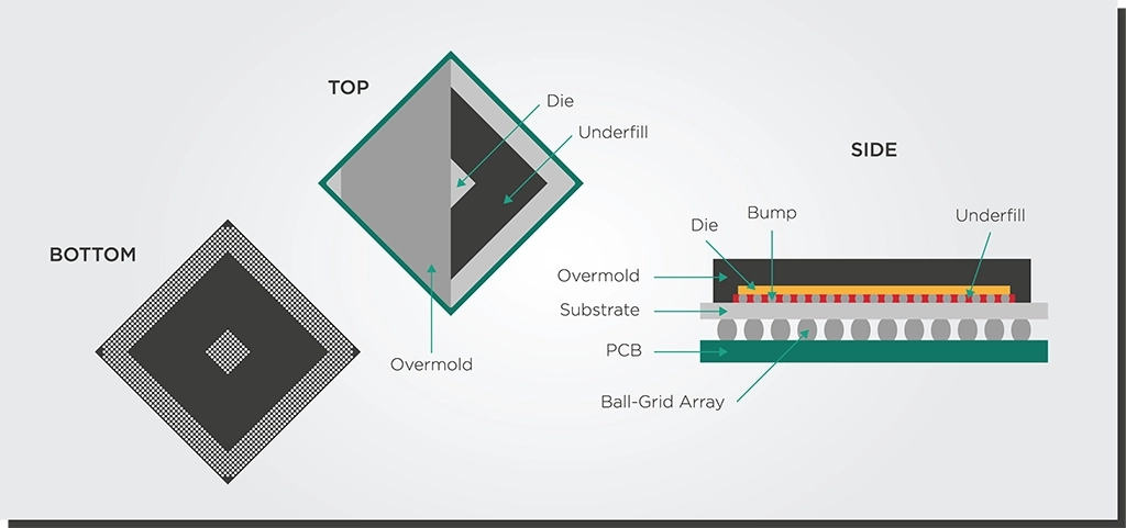
One electronic technique essential to transfer into photonics is ball-grid array (BGA) packaging. BGA-style packaging has grown popular among electronics manufacturers over the last few decades. It places the chip connections under the chip package, allowing more efficient use of space in circuit boards, a smaller package size, and better soldering.
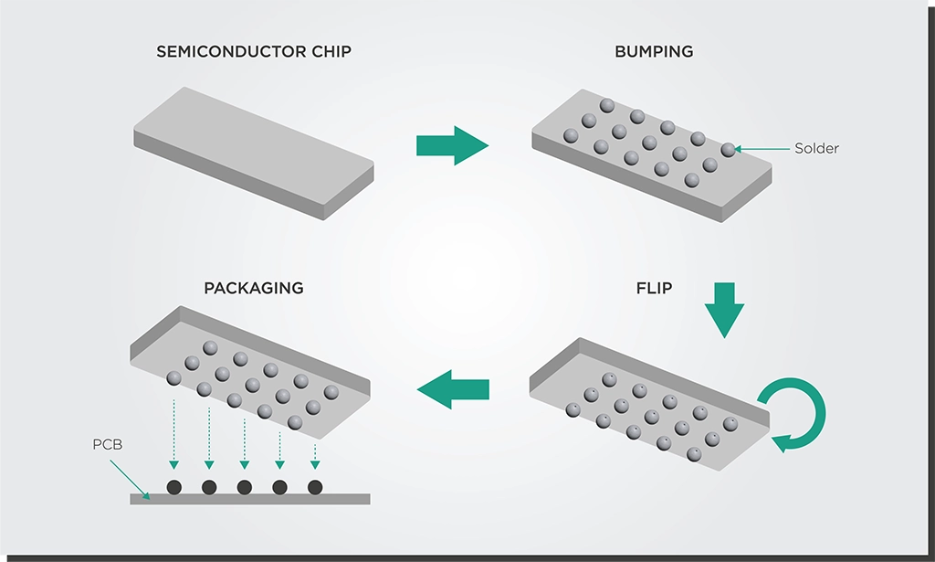
Another critical technique to move into photonics is flip-chip bonding. This process is where solder bumps are deposited on the chip in the final fabrication step. The chip is flipped over and aligned with a circuit board for easier soldering.
These might be novel technologies for photonics developers who have started implementing them in the last five or ten years. However, the electronics industry embraced these technologies 20 or 30 years ago. Making these techniques more widespread will make a massive difference in photonics’ ability to scale up and become as available as electronics.
Adopting BGA-style packaging and flip-chip bonding techniques will make it easier for PICs to survive this soldering process. There is ongoing research and development worldwide, including at EFFECT Photonics, to transfer more electronics packaging methods into photonics. PICs that can handle being soldered to circuit boards allow the industry to build optical subassemblies that are more accessible to the open market and can go into trains, cars, or airplanes.
Economics of scale is a crucial principle behind electronics manufacturing, and we must apply it to photonics too. The more components we can integrate into a single chip and the more chips we can integrate into a single wafer, the more affordable the photonic device becomes. If production volumes increase from a few thousand chips per year to a few million, the price per optical chip can decrease from thousands of Euros to mere tens of Euros. This must be the goal for the photonics industry in general.
By integrating all optical components on a single chip, we also shift the complexity from the assembly process to the much more efficient and scalable semiconductor wafer process. Assembling and packaging a device by interconnecting multiple photonic chips increases assembly complexity and costs. On the other hand, combining and aligning optical components on a wafer at a high volume is much easier, which drives down the device’s cost.
Deepening photonics integration will also have a significant impact on power consumption. Integrating all the optical components (lasers, detectors, modulators, etc.) on a single chip can minimize the losses and make devices such as optical transceivers more efficient. This approach doesn’t just optimize the efficiency of the devices themselves but also of the resource-hungry chip manufacturing process.
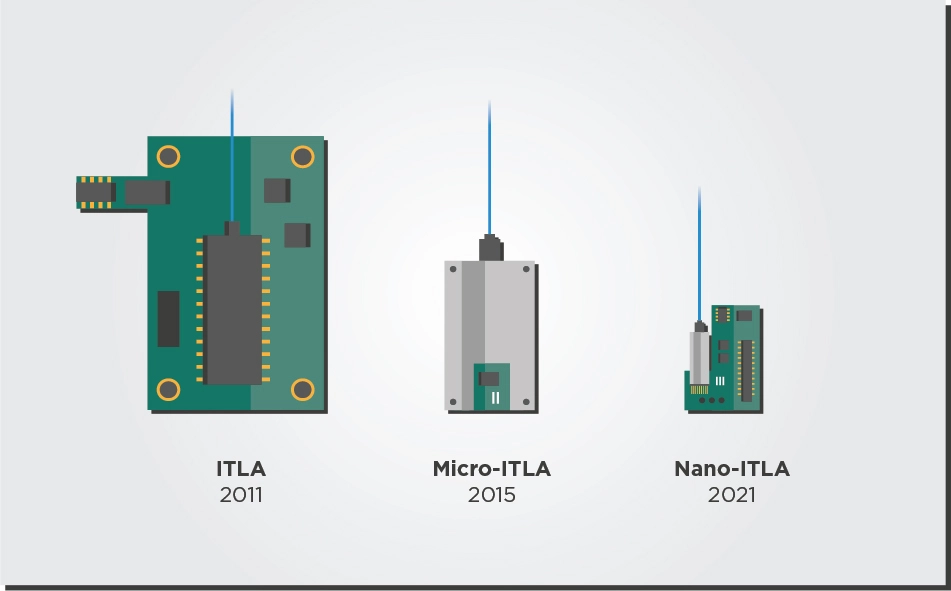
Over the last decade, technological progress in tunable laser packaging and integration has matched the need for smaller footprints. In 2011, tunable lasers followed the multi-source agreement (MSA) for integrable tunable laser assemblies (ITLAs). By 2015, tunable lasers were sold in the more compact Micro-ITLA form factor, which cut the original ITLA package size in half. And in 2019, laser developers (see examples here and here) announced a new Nano-ITLA form factor that reduced the size by almost half again.
Reducing the footprint of tunable lasers in the future will need even greater integration of their parts. For example, every tunable laser needs a wavelength locker component that can stabilize the laser’s output regardless of environmental conditions such as temperature. Integrating the wavelength locker component on the laser chip instead of attaching it externally would help reduce the laser package’s footprint and power consumption.
Another aspect of optimizing laser module footprint is allowing transceiver developers to mix and match their building blocks. For example, traditional ITLAs in transceivers contain the temperature control driver and power converter functions. However, the main transceiver board can usually provide these functions too. A setup in which the main board performs these driver and converter functions would avoid the need for redundant elements in both the main board and tunable laser.
Finally, the future of laser packaging will also involve packaging more multi-laser arrays. As explained in a previous article, multi-laser arrays will become increasingly necessary to increase link capacity in coherent systems. They will not need more slots in the router faceplate while avoiding the higher cost and complexity of increasing the speed with a single laser channel.
Improving subassemblies and packaging is vital for photonics to reach its potential. Photonics must learn from well-established, standardized electronics packaging techniques like BGA-style packaging and flip-chip bonding. By increasing integration, photonics can achieve economies of scale that make devices more affordable and energy efficient. In this context, improved integration and packaging of tunable lasers and arrays will be particularly important. Overall, these efforts will make photonics more accessible to the open market and make it as easy to manufacture and use as electronics.
Tags: Assembly, electronics, flip chip bonding, integration, Manufacturing, Packaging, Photonics, Subassemblies, testing
Photonics is one of the enabling technologies of the future. Light is the fastest information…
Photonics is one of the enabling technologies of the future. Light is the fastest information carrier in the universe and can transmit this information while dissipating less heat and energy than electrical signals. Thus, photonics can dramatically increase the speed, reach, and flexibility of communication networks and cope with the ever-growing demand for more data. And it will do so at a lower energy cost, decreasing the Internet’s carbon footprint. Meanwhile, fast and efficient photonic signals have massive potential for sensing and imaging applications in medical devices, automotive LIDAR, agricultural and food diagnostics, and more.
Given its importance, we should discuss the fabrication processes inside photonic semiconductor foundries.
Manufacturing semiconductor chips for photonics and electronics is one of the most complex procedures in the world. For example, back in his university days, EFFECT Photonics co-founder Boudewijn Docter described a fabrication process with 243 steps!
Yuqing Jiao, Associate Professor at the Eindhoven University of Technology (TU/e), explains the fabrication process in a few basic, simplified steps:
Real life is, of course, a lot more complicated and will require cycling through these steps tens of times, leading to processes with more than 200 total steps. Let’s go through these basic steps in a bit more detail.
1. Layer Epitaxy and Deposition: Different chip elements require different semiconductor material layers. These layers can be grown on the semiconductor wafer via a process called epitaxy or deposited via other methods, such as physical or chemical vapor deposition.
2. Lithography (i.e., printing): There are a few lithography methods, but the one used for high-volume chip fabrication is projection optical lithography. The semiconductor wafer is coated with aphotosensitive polymer film called a photoresist. Meanwhile, the design layout pattern is transferred to an opaque material called a mask. The optical lithography system projects the mask pattern onto the photoresist. The exposed photoresist is then developed (like photographic film) to complete the pattern printing.
3. Etching: Having “printed” the pattern on the photoresist, it is time to remove (or etch) parts of the semiconductor material to transfer the pattern from the resist into the wafer. Etching techniques can be broadly classified into two categories.
4. Cleaning and Surface Preparation: After etching, a series of steps will clean and prepare the surface before the next cycle.
Figure 5 summarizes how an InP photonic device looks after the steps of layer epitaxy, etching, dielectric deposition and planarization, and metallization.
After this fabrication process ends, the processed wafers are shipped worldwide to be tested and packaged into photonic devices. This is an expensive process we discussed in one of our previous articles.
The process of making photonic integrated circuits is incredibly long and complex, and the steps we described in this article are a mere simplification of the entire process. It requires tremendous knowledge in chip design, fabrication, and testing from experts in different fields worldwide. EFFECT Photonics was founded by people who fabricated these chips themselves, understood the process intimately and developed the connections and network to develop cutting-edge PICs at scale.
Tags: Agricultural, Carbon Footprint, Chip Material, Cleaning, Communication Networks, Deposition, Energy Cost, Epitaxy, Etching, Fabrication Process, Food Diagnostics, Integrated Photonics, LIDAR, Lithography, Manufacturing, Medical Devices, Metallization, Photonic Foundry, Photonics, Semiconductor, Sensing and Imaging, Surface Preparation
Article first published 15 June 2022, updated 18 May 2023. With the increasing demand for…
Article first published 15 June 2022, updated 18 May 2023.
With the increasing demand for cloud-based applications, datacom providers are expanding their distributed computing networks. Therefore, they and telecom provider partners are looking for data center interconnect (DCI) solutions that are faster and more affordable than before to ensure that connectivity between metro and regional facilities does not become a bottleneck.
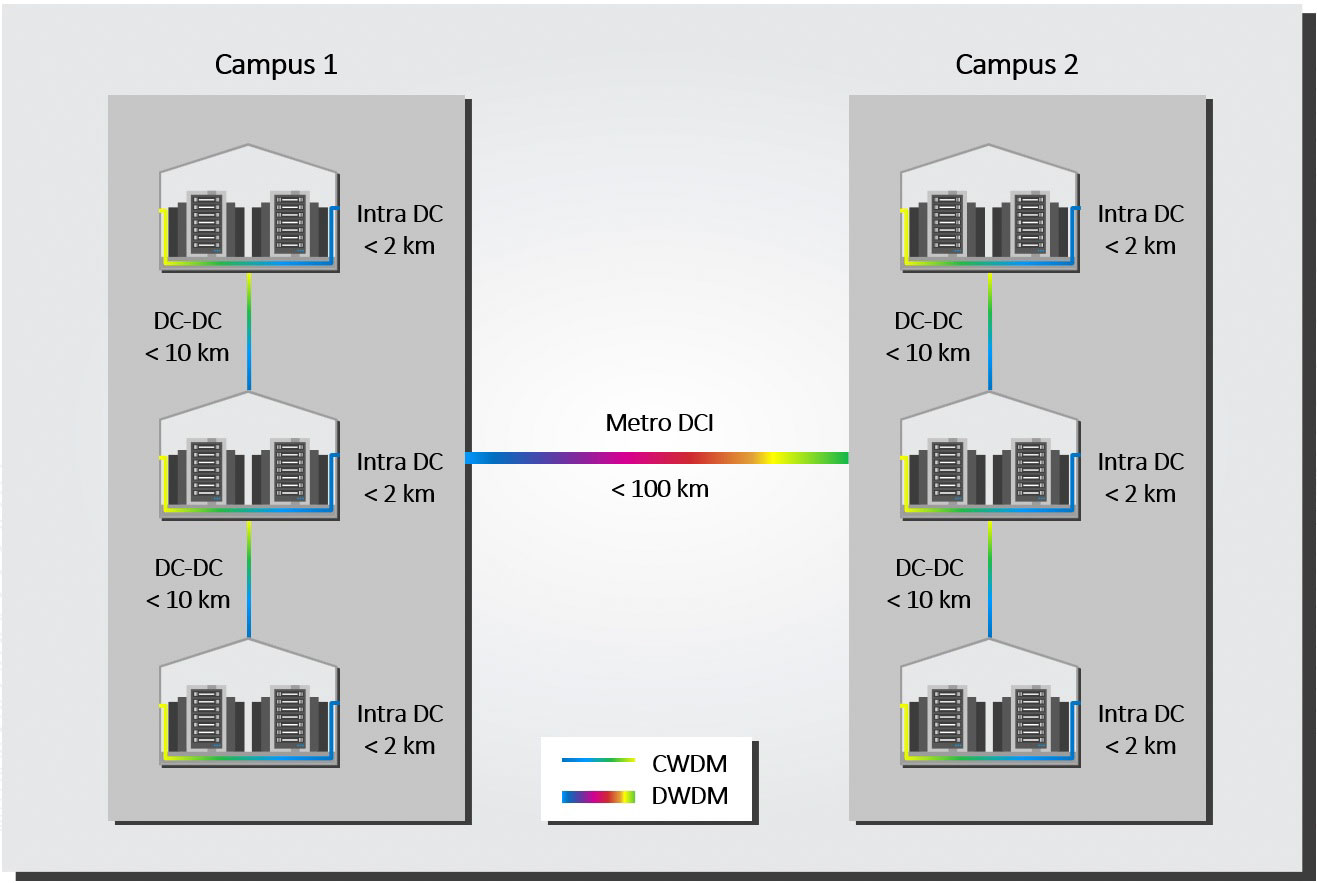
As shown in the figure below, we can think about three categories of data center interconnects based on their reach
Coherent 400ZR now dominates the metro DCI space, but in the coming decade, coherent technology could also play a role in shorter ranges, such as campus and intra-data center interconnects. As interconnects upgrade to Terabit speeds, coherent technology might start coming closer to direct detect power consumption and cost.
The advances in electronic and photonic integration allowed coherent technology for metro DCIs to be miniaturized into QSFP-DD and OSFP form factors. This progress allowed the Optical Internetworking Forum (OIF) to create a 400ZR multi-source agreement. With small enough modules to pack a router faceplate densely, the datacom sector could profit from a 400ZR solution for high-capacity data center interconnects of up to 80km. Operations teams found the simplicity of coherent pluggables very attractive. There was no need to install and maintain additional amplifiers and compensators as in direct detection: a single coherent transceiver plugged into a router could fulfill the requirements.
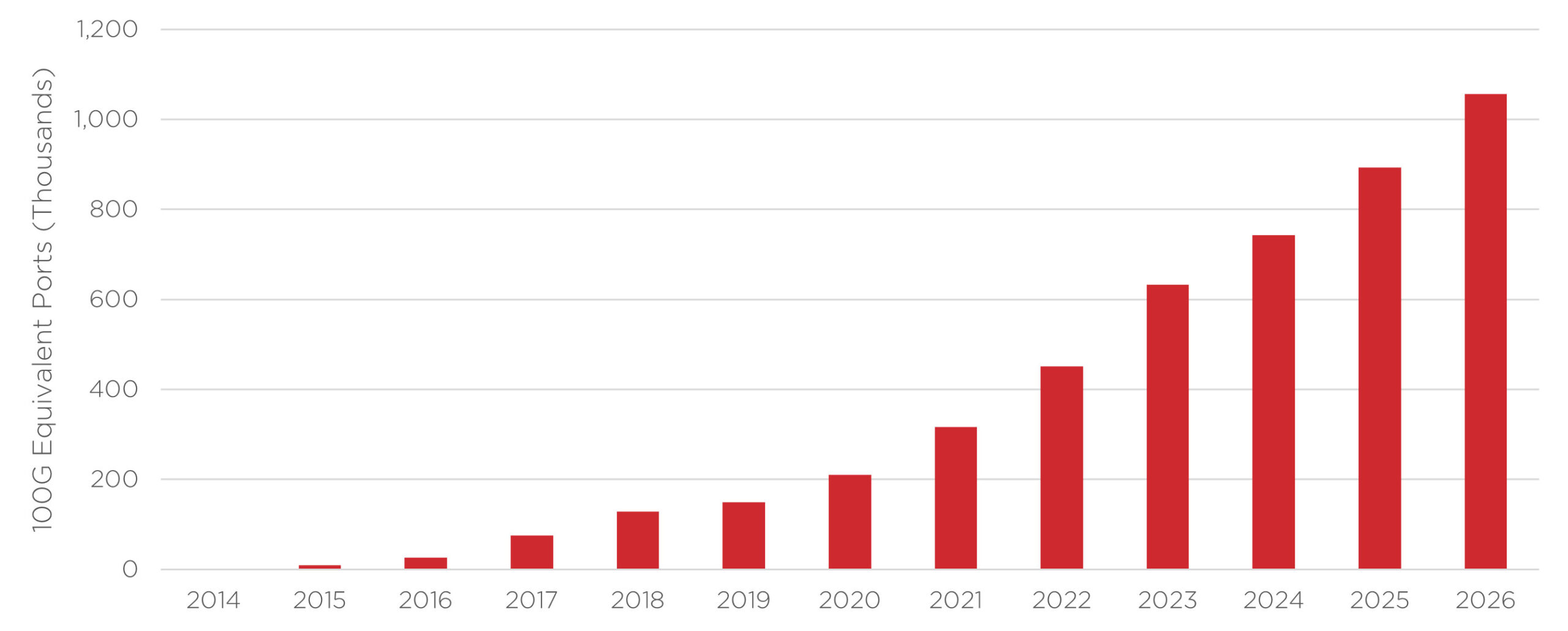
As an example of their success, Cignal AI forecasted that 400ZR shipments would dominate edge applications, as shown in Figure 2.
The campus DCI segment, featuring distances below 10 kilometers, was squarely in the domain of direct detect products when the standard speed of these links was 100Gbps. No amplifiers nor compensators were needed for these shorter distances, so direct detect transceivers are as simple to deploy and maintain as coherent ones.
However, as link bandwidths increase into the Terabit space, these direct detect links will need more amplifiers to reach 10 kilometers, and their power consumption will approach that of coherent solutions. The industry initially predicted that coherent solutions would be able to match the power consumption of PAM4 direct detect solutions as early as 800G generation. However, PAM4 developers have proven resourceful and have borrowed some aspects of coherent solutions without fully implementing a coherent solution. For example, ahead of OFC 2023, semiconductor solutions provider Marvell announced a 1.6Tbps PAM4 platform that pushes the envelope on the cost and power per bit they could offer in the 10 km range.
Following the coming years and how the PAM-4 industry evolves will be interesting. How many (power-hungry) features of coherent solutions will they have to borrow if they want to keep up in upcoming generations and speeds of 3.2 Tbps and beyond? Lumentum’s Chief Technology Officer, Brandon Collings, has some interesting thoughts on the subject in this interview with Gazettabyte.
Below Terabit speeds, direct detect technology (both NRZ and PAM-4) will likely dominate the intra-DCI space (also called data center fabric) in the coming years. In this space, links span less than 2 kilometers, and for particularly short links (< 300 meters), affordable multimode fiber (MMF) is frequently used.
Nevertheless, moving to larger, more centralized data centers (such as hyperscale) is lengthening intra-DCI links. Instead of transferring data directly from one data center building to another, new data centers move data to a central hub. So even if the building you want to connect to might be 200 meters away, the fiber runs to a hub that might be one or two kilometers away. In other words, intra-DCI links are becoming campus DCI links requiring their single-mode fiber solutions.
On top of these changes, the upgrades to Terabit speeds in the coming decade will also see coherent solutions more closely challenge the power consumption of direct detect transceivers. PAM-4 direct detect transceivers that fulfill the speed requirements require digital signal processors (DSPs) and more complex lasers that will be less efficient and affordable than previous generations of direct detect technology. With coherent technology scaling up in volume and having greater flexibility and performance, one can argue that it will also reach cost-competitiveness in this space.
Unsurprisingly, using coherent or direct detect technology for data center interconnects boils down to reach and capacity needs. 400ZR coherent is already established as the solution for metro DCIs. In campus interconnects of 10 km or less, PAM-4 products remain a robust solution up to 1.6 Tbps, but coherent technology is making a case for its use. Thus, it will be interesting to see how they compete in future generations and 3.2 Tbps.
Coherent solutions are also becoming more competitive as the intra-data center sector moves into higher Terabit speeds, like 3.2Tbps. Overall, the datacom sector is moving towards coherent technology, which is worth considering when upgrading data center links.
Tags: 800G, access networks, coherent, cost, cost-effective, Data center, distributed computing, edge and metro DCIs, integration, Intra DCI, license, metro, miniaturized, photonic integration, Photonics, pluggable, power consumption, power consumption SFP, reach, Terabit
The world is moving towards tunability. Datacom and telecom companies may increase their network capacity…
The world is moving towards tunability. Datacom and telecom companies may increase their network capacity without investing in new fiber infrastructure thanks to tunable lasers and dense wavelength division multiplexing (DWDM). Furthermore, the miniaturization of coherent technology into pluggable transceiver modules has enabled the widespread implementation of IP over DWDM solutions. Self-tuning algorithms have also contributed to the broad adoption of DWDM systems since they reduce the complexity of deployment and maintenance.
The tunable laser is a core component of all these tunable communication systems, both direct detection and coherent. The fundamental components of a laser are the following:
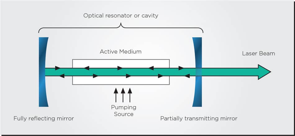
As light circulates throughout the resonator, it passes multiple times through the pumped gain medium, amplifying itself and building up power to become the highly concentrated and coherent beam of light we know as a laser.
There are multiple ways to tune lasers, but let’s discuss three common tuning methods. These methods can and are often used together.
With this short intro on how lasers work and can be tuned, let’s dive into some of the different tunable lasers used in communication systems.
Distributed Feedback (DFB) lasers are unique because they directly etch a grating onto the gain medium. This grating acts as a periodic mirror, forming the optical resonator needed to recirculate light and create a laser beam. These lasers are tunable by tuning the temperature of the gain medium and by filtering with the embedded grating.
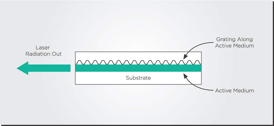
Compared to their predecessors, DFB lasers could produce very pure, high-quality laser light with lower complexity in design and manufacturing that could be easily integrated into optical fiber systems. These characteristics benefited the telecommunications sector, which needed lasers with high purity and low noise that could be produced at scale. After all, the more pure (i.e., lower linewidth) a laser is, the more information it can encode. Thus, DFB lasers became the industry’s solution for many years.
The drawback of DFB lasers is that embedding the grating element in the gain medium makes them more sensitive and unstable. This sensitivity narrows their tuning range and makes them less reliable as they age.
A simple way to improve the reliability compared to a DFB laser is to etch the grating element outside the gain medium instead of inside. This grating element (which in this case is called a Bragg reflector) acts as a mirror that creates the optical resonator and amplifies the light inside. This setup is called a distributed Bragg reflector (DBR) laser.
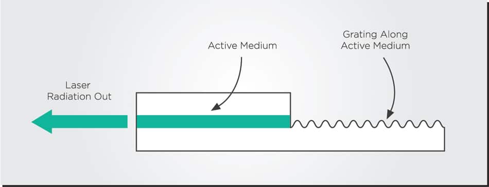
While, in principle, a DBR laser does not have a wider tuning range than a DFB laser, its tuning behavior is more reliable over time. Since the grating is outside the gain medium, the DBR laser is less sensitive to environmental fluctuations and more reliable as it ages. However, as coherent and DWDM systems became increasingly important, the industry needed a greater tuning range that DFB and DBR lasers alone could not provide.
Interestingly enough, one of the most straightforward ways to improve the quality and tunability of a semiconductor laser is to use it inside a second, somewhat larger resonator. This setup is called an external cavity laser (ECL) since this new resonator or cavity will use additional optical elements external to the original laser.
The main modification to the original semiconductor laser is that instead of having a partially reflective mirror as an output coupler, the coupler will use an anti-reflection coating to become transparent. This helps the original laser resonator capture more light from the external cavity.
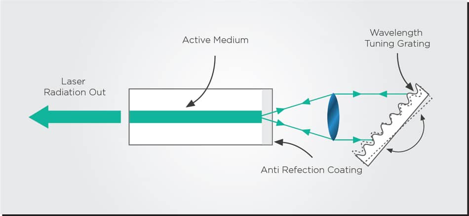
The new external resonator provides more degrees of freedom for tuning the laser. If the resonator uses a mirror, then the laser can be tuned by moving the mirror a bit and changing the length of the resonator. If the resonator uses a grating, it has an additional element to tune the laser by filtering.
ECLs have become the state-of-the-art solution in the telecom industry: they use a DFB or DBR laser as the “base laser” and external gratings as their filtering element for additional tuning. These lasers can provide a high-quality laser beam with low noise, narrow linewidth, and a wide tuning range. However, they came with a cost: manufacturing complexity.
ECLs initially required free-space bulk optical elements, such as lenses and mirrors, for the external cavity. One of the hardest things to do in photonics is coupling between free-space optics and a chip. This alignment of the free-space external cavity with the original laser chip is extremely sensitive to environmental disturbances. Therefore, their coupling is often inefficient and complicates manufacturing and assembly processes, making them much harder to scale in volume.
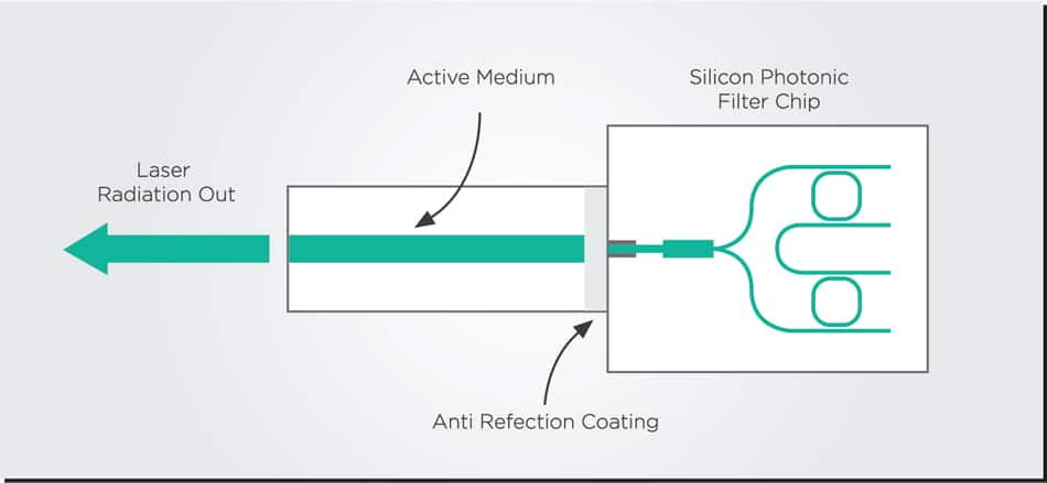
Laser developers have tried to overcome this obstacle by manufacturing the external cavity on a separate chip coupled to the original laser chip. Coupling these two chips together is still a complex problem for manufacturing but more feasible and scalable than coupling from chip to free space optics. This is the direction many major tunable laser developers will take in their future products.
As we explained in the introductory section, linear resonators are those in which light bounces back and forth between two mirrors. However, ring resonators take a different approach to feedback: the light loops multiple times inside a ring that contains the active medium. The ring is coupled to the rest of the optical circuit via a waveguide.
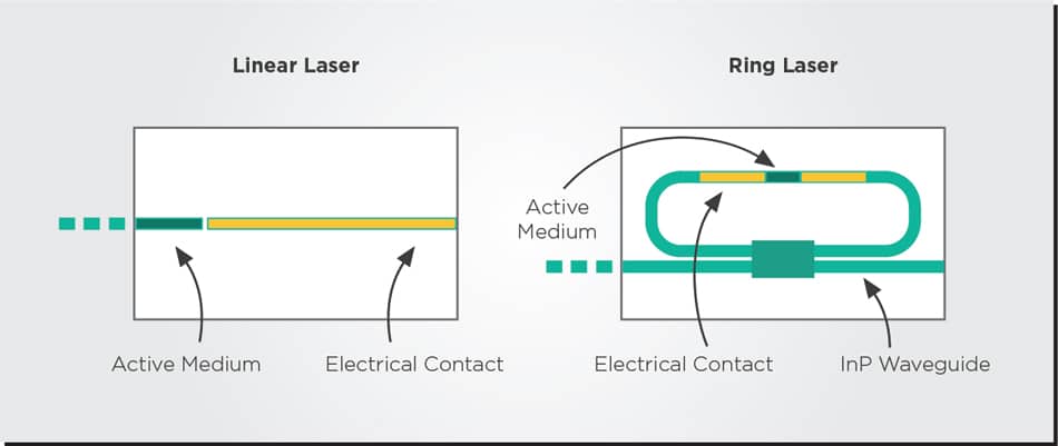
The power of the ring resonator lies in its compactness, flexibility, and integrability. While a single ring resonator is not that impressive or tunable, using multiple rings and other optical elements allows them to achieve performance and tunability on par with the state-of-the-art tunable lasers that use linear resonators.
Most importantly, these widely tunable ring lasers can be entirely constructed on a single chip of Indium Phosphide (InP) material. As shown in this paper from the Eindhoven University of Technology, these lasers can even be built with the same basic building blocks and processes used to make other elements in the InP photonic integrated circuit (PIC).
This high integration of ring lasers has many positive effects. It can avoid inefficient couplings and make the laser more energy efficient. Furthermore, it enables the development of a monolithically integrated laser module where every element is included on the same chip. This includes integrating the wavelength locker component on the same chip, an element most state-of-the-art lasers attach separately.
As we have argued in previous articles, the more elements can be integrated into a single chip, the more scalable the manufacturing process can become.
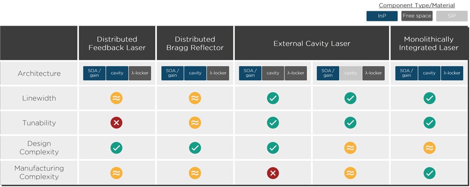
Factors such as output power, noise, linewidth, tuning range, and manufacturability are vital when deciding which kind of laser to use. A DFB or DBR laser should do the job if wide tunability is not required. Greater tuning range will require an external cavity laser, but if the device must be manufactured at a large volume, an external cavity made on a chip instead of free-space optics will scale more easily. The latter is the tunable laser solution the telecom industry is gravitating towards.
That being said, ring lasers are a promising alternative because they can enable a widely tunable and monolithically integrated laser with all elements, including wavelength locker, on the same chip. This setup is ideal for scaling into high production volumes.
Tags: EFFECT Photonics, Photonics
Today’s digital society depends heavily on securely transmitting and storing data. One of the oldest…
Today’s digital society depends heavily on securely transmitting and storing data. One of the oldest and most widely used methods to encrypt data is called RSA (Rivest-Shamir-Adleman – the surnames of the algorithm’s designers). However, in 1994 mathematician Peter Shor proved that an ideal quantum computer could find the prime factors of large numbers exponentially more quickly than a conventional computer and thus break RSA encryption within hours or days.
While practical quantum computers are likely decades away from implementing Shor’s algorithm with enough performance and scale to break RSA or similar encryption methods, the potential implications are terrifying for our digital society and our data safety.
Given these risks, arguably the most secure way to protect data and communications is by fighting quantum with quantum: protect your data from quantum computer hacking by using security protocols that harness the power of quantum physics laws. That’s what quantum key distribution (QKD) does.
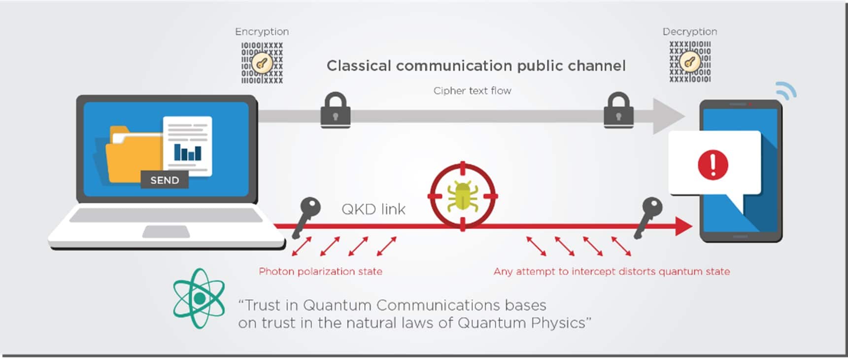
The quantum bits (qubits) used by QKD systems can be photons, electrons, atoms, or any other system that can exist in a quantum state. However, using photons as qubits will likely dominate the quantum communications and QKD application space. We have decades of experience manipulating the properties of photons, such as polarization and phase, to encode qubits. Thanks to optical fiber, we also know how to send photons over long distances with relatively little loss. Besides, optical fiber is already a fundamental component of modern telecommunication networks, so future quantum networks can run on that existing fiber infrastructure. All these signs point towards a new era of quantum photonics.
Photonic QKD devices have been, in some shape or form, commercially available for over 15 years. Still, factors such as the high cost, large size, and the inability to operate over longer distances have slowed their widespread adoption. Many R&D efforts regarding quantum photonics aim to address the size, weight, and power (SWaP) limitations. One way to overcome these limitations and reduce the cost per device would be to integrate every QKD function—generating, manipulating, and detecting photonic qubits—into a single chip.
Bringing quantum products from lab prototypes to fully realized products that can be sold on the market is a complex process that involves several key steps.
One of the biggest challenges in bringing quantum products to market is scaling up the technology from lab prototypes to large-scale production. This requires the development of reliable manufacturing processes and supply chains that can produce high-quality quantum products at scale. Quantum products must be highly performant and reliable to meet the demands of commercial applications. This requires extensive testing and optimization to ensure that the product meets or exceeds the desired specifications.
In addition, quantum products must comply with relevant industry standards and regulations to ensure safety, interoperability, and compatibility with existing infrastructure. This requires close collaboration with regulatory bodies and industry organizations to develop appropriate standards and guidelines.
Photonic integration is a process that makes these goals more attainable for quantum technologies. By taking advantage of existing semiconductor manufacturing systems, quantum technologies can more scale up their production volumes more easily.
One of the most significant advantages of integrated photonics is its ability to miniaturize optical components and systems, making them much smaller, lighter, and more portable than traditional optical devices. This is achieved by leveraging micro- and nano-scale fabrication techniques to create optical components on a chip, which can then be integrated with other electronic and optical components to create a fully functional device.
The miniaturization of optical components and systems is essential for the development of practical quantum technologies, which require compact and portable devices that can be easily integrated into existing systems. For example, compact and portable quantum sensors can be used for medical imaging, geological exploration, and industrial process monitoring. Miniaturized quantum communication devices can be used to secure communication networks and enable secure communication between devices.
Integrated photonics also allows for the creation of complex optical circuits that can be easily integrated with other electronic components, to create fully integrated opto-electronic quantum systems. This is essential for the development of practical quantum computers, which require the integration of a large number of qubits (quantum bits) with control and readout electronics.
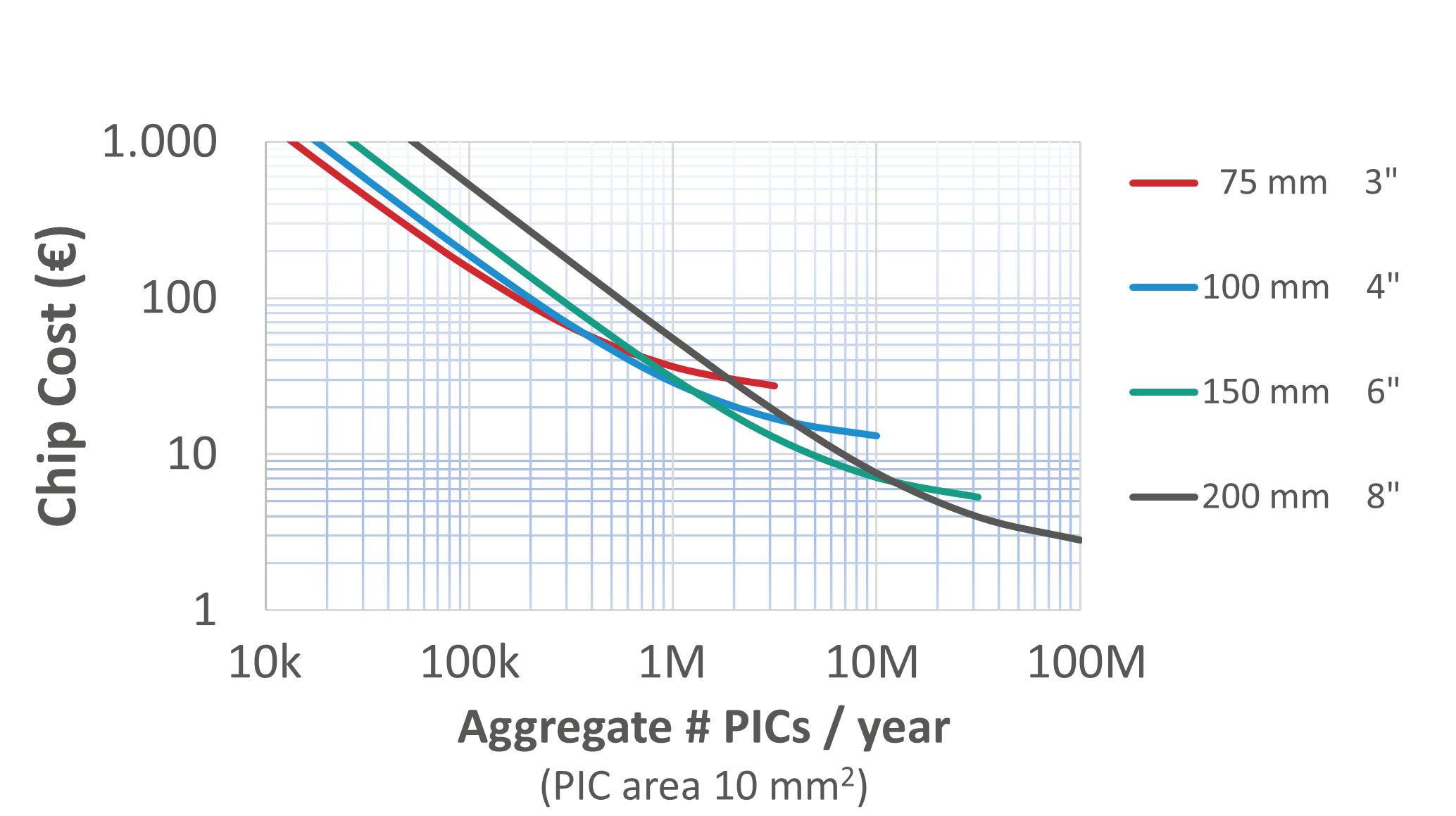
Wafer scale photonics manufacturing demands a higher upfront investment, but the resulting high-volume production line drives down the cost per device. This economy-of-scale principle is the same one behind electronics manufacturing, and the same must be applied to photonics. The more optical components we can integrate into a single chip, the more can the price of each component decrease. The more optical System-on-Chip (SoC) devices can go into a single wafer, the more can the price of each SoC decrease.
Researchers at the Technical University of Eindhoven and the JePPIX consortium have done some modelling to show how this economy of scale principle would apply to photonics. If production volumes can increase from a few thousands of chips per year to a few millions, the price per optical chip can decrease from thousands of Euros to mere tens of Euros. This must be the goal for the quantum photonics industry.
By integrating all optical components on a single chip, we also shift the complexity from the assembly process to the much more efficient and scalable semiconductor wafer process. Assembling and packaging a device by interconnecting multiple photonic chips increases assembly complexity and costs. On the other hand, combining and aligning optical components on a wafer at a high volume is much easier, which drives down the device’s cost.
Overall, bringing quantum products to market requires a multi-disciplinary approach that involves collaboration between scientists, engineers, designers, business professionals, and regulatory bodies to develop and commercialize a high-quality product that meets the needs of its target audience. Integrated photonics offers significant advantages in miniaturization and scale-up potential, which are essential in taking quantum technologies from the lab to the market.
Tags: Economy-of-scale, EFFECT Photonics, Integrated Photonics, miniaturization, Photonics, Photons, Quantum, Quantum products, Qubits, RSA encryption, Wafer Scale Photonics
The demand for data and other digital services is rising exponentially. From 2010 to 2020,…
The demand for data and other digital services is rising exponentially. From 2010 to 2020, Internet users worldwide doubled, and global internet traffic increased 12-fold. From 2020 to 2026, internet traffic will likely increase 5-fold. To meet this demand, datacom and telecom operators need constantly upgrade their transport networks.
The major obstacles in this upgrade path remain the power consumption, thermal management, and affordability of transceivers. Over the last two decades, power ratings for pluggable modules have increased as we moved from direct detection to more power-hungry coherent transmission: from 2W for SFP modules to 3.5 W for QSFP modules and now to 14W for QSSFP-DD and 21.1W for OSFP form factors. This power consumption increase seems incompatible with the power constraints of the network edge.
This article will review trends in data rate, power consumption, and footprint for transceivers in the network edge that aim to address these challenges.
Given the success of 400ZR pluggable coherent solutions in the market, discussions in the telecom sector about a future beyond 400G pluggables have often focused on 800G solutions and 800ZR. However, there is also increasing excitement about “downscaling” to 100G coherent products for applications in the network edge.
In the coming years, 100G coherent uplinks will become increasingly widespread in deployments and applications throughout the network edge. Some mobile access networks use cases must upgrade their existing 10G DWDM link aggregation into a single coherent 100G DWDM uplink. Meanwhile, cable networks and business services are upgrading their customer links from 1Gbps to 10Gbps, and this migration will be the significant factor that will increase the demand for coherent 100G uplinks. For carriers who provide converged cable/mobile access, these upgrades to 100G uplinks will enable opportunities to overlay more business services and mobile traffic into their existing cable networks.
You can read more about these developments in our previous article, When Will the Network Edge Go Coherent?
Data centers and 5G networks might be hot commodities, but the infrastructure that enables them runs even hotter. Electronic equipment generates plenty of heat; the more heat energy an electronic device dissipates, the more money and energy must be spent to cool it down. These power efficiency issues do not just affect the environment but also the bottom lines of communications companies.
As shown in the table below, the growth of data centers and wireless networks will continue to drive power consumption upwards.

These power constraints are even more pressing in the access network sector. Unlike data centers and the network core, access network equipment lives in uncontrolled environments with limited cooling capabilities. Therefore, every extra watt of pluggable power consumption will impact how vendors and operators design their cabinets and equipment.
These struggles are a major reason why QSFP28 form factor solutions are becoming increasingly attractive in the 100ZR domain. Their power consumption (up to 6 watts) is lower than that of QSFP-DD form factors (up to 14 Watts), which allows them to be stacked more densely in access network equipment rooms. Besides, QSFP28 modules are compatible with existing access network equipment, which often features QSFP28 slots.
Aside from the move to QSFP28 form factors for 100G coherent, EFFECT Photonics also believes in two other ways to reduce power consumption.
Moving toward smaller pluggable footprints should not necessarily be a goal, but as we mentioned in the previous section, it is a means toward the goal of lower power consumption. Decreasing the size of optical components and their interconnections means that the light inside the chip will travel a smaller distance and accumulate fewer optical losses.
Let’s look at an example of lasers. In the last decade, technological progress in tunable laser packaging and integration has matched the need for smaller footprints. In 2011, tunable lasers followed the multi-source agreement (MSA) for integrable tunable laser assemblies (ITLAs). The ITLA package measured around 30.5 mm in width and 74 mm in length. By 2015, tunable lasers were sold in the more compact Micro-ITLA form factor, which cut the original ITLA package size in half. And in 2019, laser developers (see examples here and here) announced a new Nano-ITLA form factor that reduced the size by almost half again.
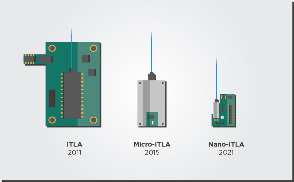
Reducing the footprint of tunable lasers in the future will need even greater integration of their parts. For example, every tunable laser needs a wavelength locker component that can stabilize the laser’s output regardless of environmental conditions such as temperature. Integrating the wavelength locker component on the laser chip instead of attaching it externally would help reduce the laser package’s footprint and power consumption.
Another potential future to reduce the size of tunable laser packages is related to the control electronics. The current ITLA standards include the complete control electronics on the laser package, including power conversion and temperature control. However, if the transceiver’s main board handles some of these electronic functions instead of the laser package, the size of the laser package can be reduced.
This approach means the reduced laser package would only have full functionality if connected to the main transceiver board. However, some transceiver developers will appreciate the laser package reduction and the extra freedom to provide their own laser control electronics.
The ever-increasing bandwidth demands in access networks force coherent pluggables to face the complex problem of maintaining a good enough performance while moving to lower cost and power consumption.
The move towards 100G coherent solutions in QSFP28 form factors will play a major role in meeting the power requirements of the access network sector. Further gains can be achieved with greater integration of optical components and co-designing the optics and electronic engines of the transceiver to reduce inefficiencies. Further gains in footprint for transceivers can also be obtained by eliminating redundant laser control functions in both the laser package and the main transceiver board.
Tags: 100G Coherent Products, 400ZR Pluggable Coherent Solutions, 5G Networks, 800G Solutions, 800ZR, Affordability, Coherent Transceivers, datacom, Direct Detection, EFFECT Photonics, Internet Traffic, network edge, OSFP Form Factors, Photonics, Pluggable Modules, power consumption, Power Efficiency, QSFP Modules, QSSFP-DD, Telecom Operators, Thermal Management
Data centers and 5G networks might be hot commodities, but the infrastructure that enables them…
Data centers and 5G networks might be hot commodities, but the infrastructure that enables them runs even hotter. Electronic equipment generates plenty of heat; the more heat energy an electronic device dissipates, the more money and energy must be spent to cool it down.
The Uptime Institute estimates that the average power usage effectiveness (PUE) ratio for data centers in 2022 is 1.55. This implies that for every 1 kWh used to power data center equipment, an extra 0.55 kWh—about 35% of total power consumption—is needed to power auxiliary equipment like lighting and, more importantly, cooling. While the advent of centralized hyperscale data centers will improve energy efficiency in the coming decade, that trend is offset by the construction of many smaller local data centers on the network edge to address the exponential growth of 5G services such as the Internet of Things (IoT).
These opposing trends are one of the reasons why the Uptime Institute has only observed a marginal improvement of 10% in the average data center PUE since 2014 (which was 1.7 back then). Such a slow improvement in average data center power efficiency cannot compensate for the fast growth of new edge data centers.
For all the bad reputation data centers receive for their energy consumption, though, wireless transmission generates even more heat than wired links. While 5G standards are more energy-efficient per bit than 4G, Huawei expects that the maximum power consumption of one of their 5G base stations will be 68% higher than their 4G stations. To make things worse, the use of higher frequency spectrum bands and new IoT use cases require the deployment of more base stations too.
Prof. Earl McCune from TU Delft estimates that nine out of ten watts of electrical power in 5G systems turn into heat. This Huawei study also predicts that the energy consumption of wireless access networks will increase even more quickly than data centers in the next ten years—more than quadrupling between 2020 and 2030.
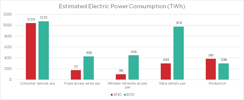
These power efficiency issues do not just affect the environment but also the bottom lines of communications companies. In such a scenario, saving even one watt of power per pluggable transceiver could quickly multiply and scale up into a massive improvement on the sustainability and profitability of telecom and datacom providers.
Let’s discuss an example to show how a seemingly small improvement of one Watt in pluggable transceiver power consumption can quickly scale up into major energy savings.
A 2020 paper from Microsoft Research estimates that for a metropolitan region of 10 data centers with 16 fiber pairs each and 100-GHz DWDM per fiber, the regional interconnect network needs to host 12,800 transceivers. This number of transceivers could increase by a third in the coming years since the 400ZR transceiver ecosystem supports a denser 75 GHz DWDM grid, so this number of transceivers would increase to 17,000. Therefore, saving a watt of power in each transceiver would lead to a total of 17 kW in savings.
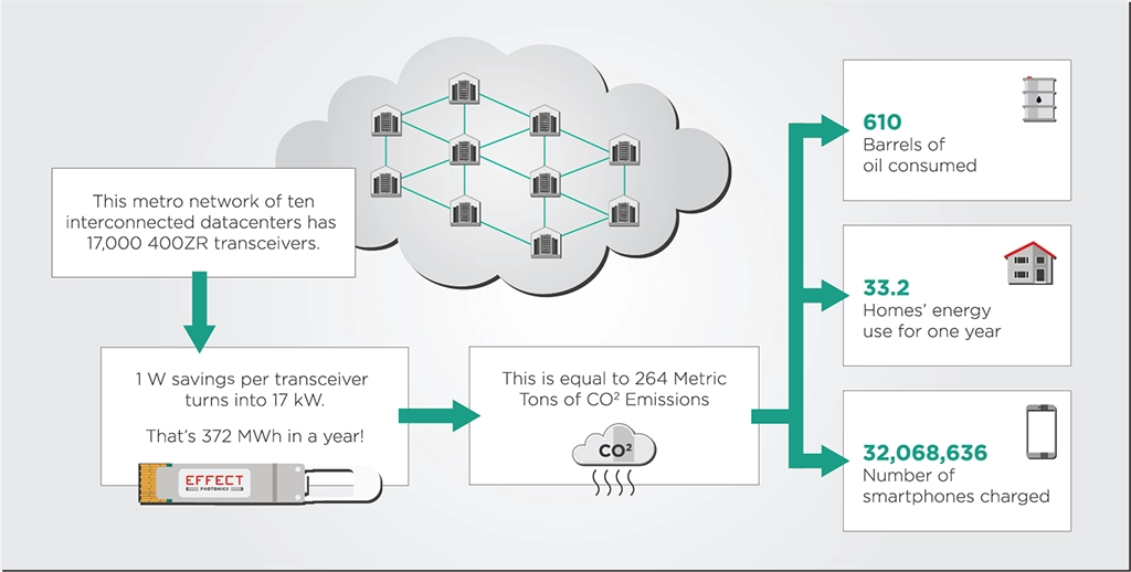
The power savings don’t end there, however. The transceiver is powered by the server, which is then powered by its power supply and, ultimately, the national electricity grid. On average, 2.5 Watts must be supplied from the national grid for every watt of power the transceiver uses. When applying that 2.5 factor, the 17 kW in savings we discussed earlier are, in reality, 42.5 kW. In a year of power consumption, this rate adds up to a total of 372 MWh in power consumption savings. According to the US Environmental Protection Agency (EPA), these amounts of power savings in a single metro data center network are equivalent to 264 metric tons of carbon dioxide emissions. These emissions are equivalent to consuming 610 barrels of oil and could power up to 33 American homes for a year.
Before 2020, Apple made its computer processors with discrete components. In other words, electronic components were manufactured on separate chips, and then these chips were assembled into a single package. However, the interconnections between the chips produced losses and incompatibilities that made their devices less energy efficient. After 2020, starting with Apple’s M1 processor, they fully integrate all components on a single chip, avoiding losses and incompatibilities. As shown in the table below, this electronic system-on-chip (SoC) consumes a third of the power compared to the processors with discrete components used in their previous generations of computers.
| 𝗠𝗮𝗰 𝗠𝗶𝗻𝗶 𝗠𝗼𝗱𝗲𝗹 | 𝗣𝗼𝘄𝗲𝗿 𝗖𝗼𝗻𝘀𝘂𝗺𝗽𝘁𝗶𝗼𝗻 | |
| 𝗜𝗱𝗹𝗲 | 𝗠𝗮𝘅 | |
| 2023, M2 | 7 | 5 |
| 2020, M1 | 7 | 39 |
| 2018, Core i7 | 20 | 122 |
| 2014, Core i5 | 6 | 85 |
| 2010, Core 2 Duo | 10 | 85 |
| 2006, Core Solo or Duo | 23 | 110 |
| 2005, PowerPC G4 | 32 | 85 |
| Table 1: Comparing the power consumption of a Mac Mini with an M1 and M2 SoC chips to previous generations of Mac Minis. [Source: Apple’s website] | ||
The photonics industry would benefit from a similar goal: implementing a photonic system-on-chip. Integrating all the optical components (lasers, detectors, modulators, etc.) on a single chip can minimize the losses and make devices such as optical transceivers more efficient. This approach doesn’t just optimize the efficiency of the devices themselves but also of the resource-hungry chip manufacturing process. For example, a system-on-chip approach enables earlier optical testing on the semiconductor wafer and dies. By testing the dies and wafers directly before packaging, manufacturers need only discard the bad dies rather than the whole package, which saves valuable energy and materials. You can read our previous article on the subject to know more about the energy efficiency benefits of system-on-chip integration.
Another way of improving power consumption in photonic devices is co-designing their optical and electronic systems. A co-design approach helps identify in greater detail the trade-offs between various parameters in the optics and electronics, optimizing their fit with each other and ultimately improving the overall power efficiency of the device. In the case of coherent optical transceivers, an electronic digital signal processor specifically optimized to drive an indium-phosphide optical engine directly could lead to power savings.
System-on-chip (SoC) approaches might reduce not only the footprint and energy consumption of photonic devices but also their cost. The economics of scale principles that rule the electronic semiconductor industry can also reduce the cost of photonic systems-on-chip. After all, SoCs minimize the footprint of photonic devices, allowing photonics developers to fit more of them within a single wafer, which decreases the price of each photonic system. As the graphic below shows, the more chips and wafers are produced, the lower the cost per chip becomes.
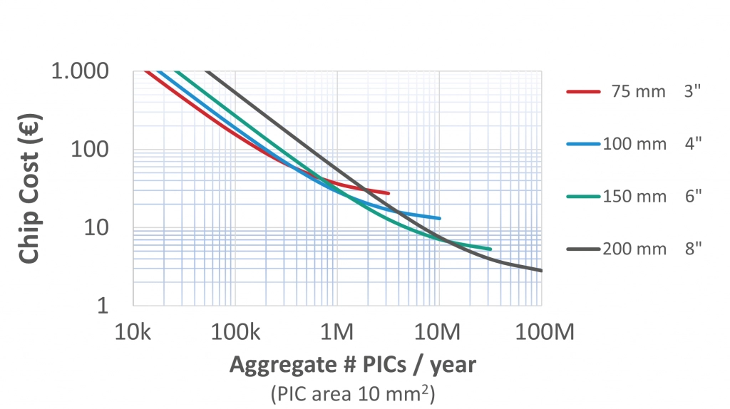
Integrating all optical components—including the laser—on a single chip shifts the complexity from the expensive assembly and packaging process to the more affordable and scalable semiconductor wafer process. For example, it’s much easier to combine optical components on a wafer at a high volume than to align components from different chips together in the assembly process. This shift to wafer processes also helps drive down the cost of the device.
With data and energy demands rising yearly, telecom and datacom providers are constantly finding ways to reduce their power and cost per transmitted bit. As we showed earlier in this article, even one watt of power saved in an optical transceiver can snowball into major savings that providers and the environment can profit from. These improvements in the power consumption of optical transceivers can be achieved by deepening the integration of optical components and co-designing them with electronics. Highly compact and integrated optical systems can also be manufactured at greater scale and efficiency, reducing their financial and environmental costs. These details help paint a bigger picture for providers: sustainability now goes hand-in-hand with profitability.
Tags: 5G, data centers, EFFECT Photonics, efficiency, energy consumption, Photonics, Sustainability, Transceivers
– Lightwave

Article first published 27 July 2022, updated 12 April 2023. Network carriers want to provide…
Article first published 27 July 2022, updated 12 April 2023.
Network carriers want to provide communications solutions in all areas: mobile access, cable networks, and fixed access to business customers. They want to provide this extra capacity and innovative and personalized connectivity and entertainment services to their customers.
Deploying only legacy direct detect technologies will not be enough to cover these growing bandwidth and service demands of mobile, cable, and business access networks with the required reach. In several cases, networks must deploy more 100G coherent dense wavelength division multiplexing (DWDM) technology to transmit more information over long distances. Several applications in the optical network edge could benefit from upgrading from 10G DWDM or 100G grey aggregation uplinks to 100G DWDM optics:
However, network providers have often stuck to their 10G DWDM or 100G grey links because the existing 100G DWDM solutions could not check all the required boxes. “Scaled-down” coherent 400ZR solutions had the required reach and tunability but were too expensive and power-hungry for many access network applications. Besides, ports in small to medium IP routers used in most edge deployments often do not support the QSFP-DD form factor commonly used in 400ZR modules but the QSFP28 form factor.
Fortunately, the rise of 100ZR solutions in the QSFP28 form factor is changing the landscape for access networks. “The access market needs a simple, pluggable, low-cost upgrade to the 10G DWDM optics that it has been using for years. 100ZR is that upgrade,” said Scott Wilkinson, Lead Analyst for Optical Components at market research firm Cignal AI. “As access networks migrate from 1G solutions to 10G solutions, 100ZR will be a critical enabling technology.”
In this article, we will discuss how the recent advances in 100ZR solutions will enable the evolution of different segments of the network edge: mobile midhaul and backhaul, business services, and cable.
The upgrade from 4G to 5G has shifted the radio access network (RAN) from a two-level structure with backhaul and fronthaul in 4G to a three-level structure with back-, mid-, and fronthaul:
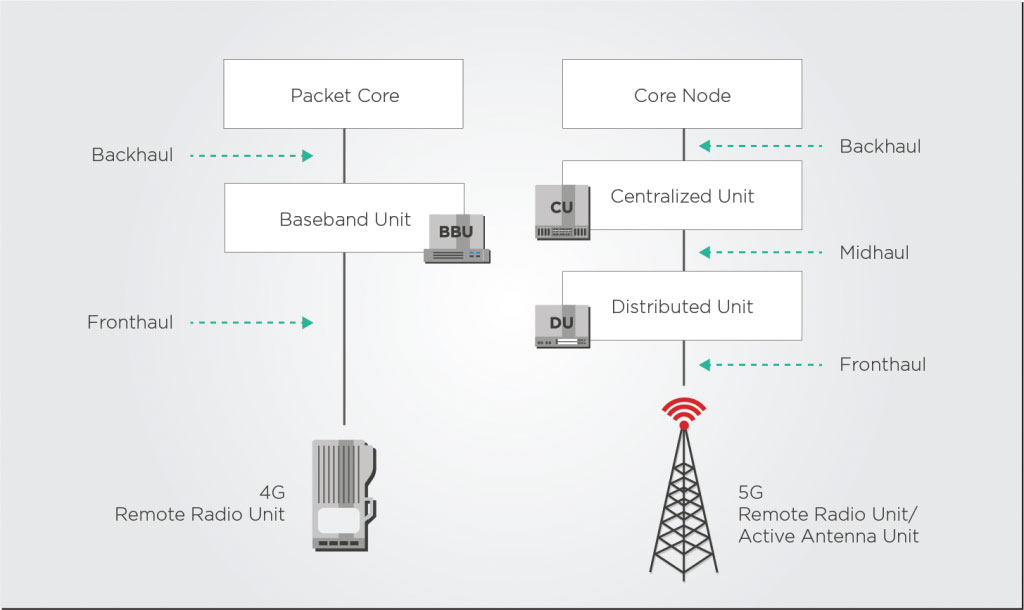
The initial rollout of 5G has already happened in most developed countries, with many operators upgrading their 1G SFPs transceiver to 10G SFP+ devices. Some of these 10G solutions had DWDM technology; many were single-channel grey transceivers. However, mobile networks must move to the next phase of 5G deployments, which requires installing and aggregating more and smaller base stations to exponentially increase the number of devices connected to the network.
These mature phases of 5G deployment will require operators to continue scaling fiber capacity cost-effectively with more widespread 10G DWDM SFP+ solutions and 25G SFP28 transceivers. These upgrades will put greater pressure on the aggregation segments of mobile backhaul and midhaul. These network segments commonly used link aggregation of multiple 10G DWDM links into a higher bandwidth group (such as 4x10G). However, this link aggregation requires splitting up larger traffic streams and can be complex to integrate across an access ring. A single 100G uplink would reduce the need for such link aggregation and simplify the network setup and operations. If you want to know more about the potential market and reach of this link aggregation upgrade, we recommend reading the recent Cignal AI report on 100ZR technologies.
According to Cignal AI’s 100ZR report, the biggest driver of 100ZR use will come from multiplexing fixed access network links upgrading from 1G to 10G. This trend will be reflected in cable networks’ long-awaited migration from Gigabit Passive Optical Networks (GPON) to 10G PON. This evolution is primarily guided by the new DOCSIS 4.0 standard, which promises 10Gbps download speeds for customers and will require several hardware upgrades in cable networks.
To multiplex these new larger 10Gbps customer links, cable providers and network operators need to upgrade their optical line terminals (OLTs) and Converged Cable Access Platforms (CCAPs) from 10G to 100G DWDM uplinks. Many of these new optical hubs will support up to 40 or 80 optical distribution networks (ODNs), too, so the previous approach of aggregating multiple 10G DWDM uplinks will not be enough to handle this increased capacity and higher number of channels.
Anticipating such needs, the non-profit R&D organization CableLabs has recently pushed to develop a 100G Coherent PON (C-PON) standard. Their proposal offers 100 Gbps per wavelength at a maximum reach of 80 km and up to a 1:512 split ratio. CableLabs anticipates C-PON and its 100G capabilities will play a significant role not just in cable optical network aggregation but in other use cases such as mobile x-haul, fiber-to-the-building (FTTB), long-reach rural scenarios, and distributed access networks.
Almost every organization uses the cloud in some capacity, whether for development and test resources or software-as-a-service applications. While the cost and flexibility of the cloud are compelling, its use requires fast, high-bandwidth wide-area connectivity to make cloud-based applications work as they should.
Similarly to cable networks, these needs will require enterprises to upgrade their existing 1G Ethernet private lines to 10G Ethernet, which will also drive a greater need for 100G coherent uplinks. Cable providers and operators will also want to take advantage of their upgraded 10G PON networks and expand the reach and capacity of their business services.
The business and enterprise services sector was the earliest adopter of 100G coherent uplinks, deploying “scaled-down” 400ZR transceivers in the QSFP-DD form factor since they were the solution available at the time. However, these QSFP-DD slots also support QSFP28 form factors, so the rise of QSFP 100ZR solutions will provide these enterprise applications with a more attractive upgrade with lower cost and power consumption. These QSFP28 solutions had struggled to become more widespread before because they required the development of new, low-power digital signal processors (DSPs), but DSP developers and vendors are keenly jumping on board the 100ZR train and have announced their development projects: Acacia, Coherent/ADVA, Marvell/InnoLight, and Marvell/OE Solutions. This is also why EFFECT Photonics has announced its plans to co-develop a 100G DSP with Credo Semiconductor that best fits 100ZR solutions in the QSFP28 form factor.
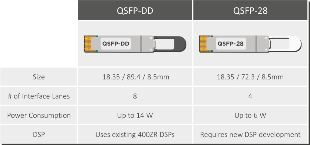
In the coming years, 100G coherent uplinks will become increasingly widespread in deployments and applications throughout the network edge. Some mobile access networks use cases must upgrade their existing 10G DWDM link aggregation into a single coherent 100G DWDM uplink. Meanwhile, cable networks and business services are upgrading their customer links from 1Gbps to 10Gbps, and this migration will be the major factor that will increase the demand for coherent 100G uplinks. For carriers who provide converged cable/mobile access, these upgrades to 100G uplinks will enable opportunities to overlay more business services and mobile traffic into their existing cable networks.
As the QSFP28 100ZR ecosystem expands, production will scale up, and these solutions will become more widespread and affordable, opening up even more use cases in access networks.
Tags: 5G, access, aggregation, backhaul, capacity, DWDM, fronthaul, Integrated Photonics, LightCounting, metro, midhaul, mobile, mobile access, network, optical networking, optical technology, photonic integrated chip, photonic integration, Photonics, PIC, PON, programmable photonic system-on-chip, solutions, technology© 2024 EFFECT PHOTONICS All rights reserved. T&C of Website - T&C of Purchase - Privacy Policy - Cookie Policy - Supplier Code of Conduct