EINDHOVEN- Over the years, The Netherlands has built up a strong reputation for academic and…
EINDHOVEN- Over the years, The Netherlands has built up a strong reputation for academic and industrial research in integrated photonics. This started in the 90s with several entities around Twente University working on glass-based optical channels, which later became the basis of the silicon-nitride-based Triplex platform developed by Lionix. Meanwhile, Philips was working on lasers for the first transatlantic optical fibre cables, which later became the basis of the Indium-Phosphide-based technology platform developed at TU (Technical University) Eindhoven. Two companies emerged from this TU Eindhoven photonics cluster: EFFECT Photonics and SMART Photonics. Where SMART Photonics focuses on making photonic chips for a wide range of customers from different application areas, and therefore pursues a foundry business model, EFFECT Photonics focuses instead on developing products purely for the telecommunications market, using external partners for the chip production – the so-called ‘fabless’ semiconductor model.
EFFECT Photonics started as a design house. Since its first venture capital investment in 2015, the company has been set on a course to develop its own products for the fibre-optic telecom market. Its focus is on medium-distance communications; typically this means distances of 10 to 100 km, where existing data links need to be upgraded from, for example, 10 Gb/s today to several hundreds of Gb/s tomorrow, to cope with the increased demand for data bandwidth that is expected from the introduction of 5G networks. Operators do not want to install new fibres, but prefer to use the existing fibre infrastructure more efficiently. EFFECT Photonics products achieve this by sending multiple colours of light through a single fibre, allowing multiple parallel streams of high-speed data to travel through the same network without interfering with each other. Customers do not need to change anything on the fibre itself: they just have to replace some equipment at the start and end of the fibre. Today’s optical chip technology allows the company to deliver this extra functionality without increasing the cost of the optics.
“When we started with EFFECT Photonics , the technology was very much still in its research phase” says Boudewijn Docter, President and co-founder of EFFECT Photonics. “The academics were working on new building blocks all the time, adding novel functions and features and publishing nice results, but not really taking the time to solidify the process and make a stronger, more reproducible baseline. Working on a new project is of course much more exciting! In addition, this is also the kind of work for which the universities can typically get their research funding. So when we started working on making a real product, we found out that first we had to go back to the basics to make sure we could make the fundamental building blocks more reproducible and better optimised for our application. It took us several years to get everything to the level where it needed to be to achieve sufficient performance from all building blocks, while being able to produce things in one process flow.”
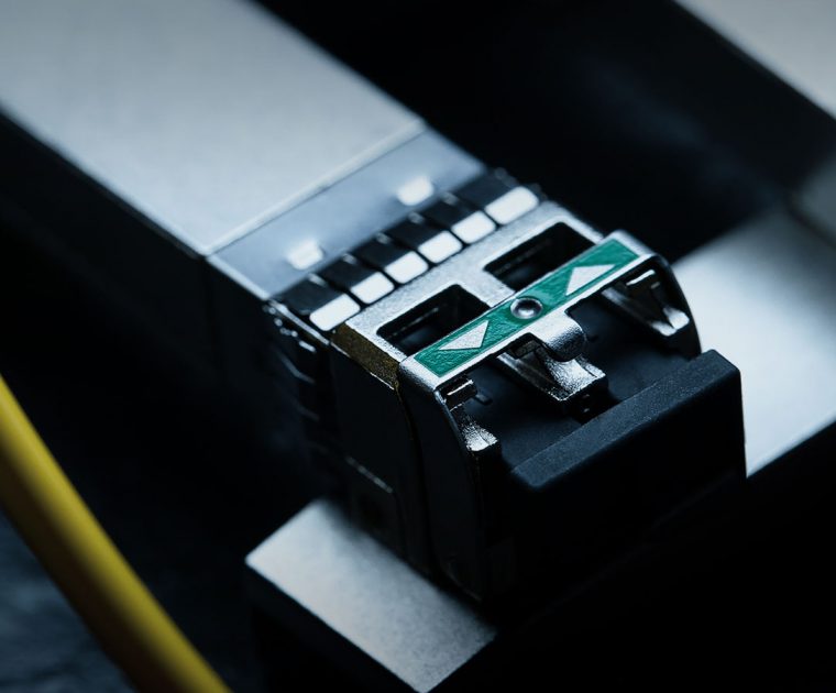
Although the optical chip is the core of the transceiver products that EFFECT Photonics makes, the innovation doesn’t stop there. The light still needs to get from the chip into the optical fibre, and the high-speed electrical data signals still need to get in and out of the chip as well. The present challenges in photonics packaging are much greater than in traditional electronics packaging. Not only is the fibre a fragile and sensitive component, but the alignments require sub-micrometre precision and the assembly needs to stay stable over widely varying ranges of temperature and other environmental conditions. “When we initially started this challenge, we first looked at external partners to work with, but in those days there were no specialised optical packing companies out there. There were a few players that could do single laser component packaging, but our chips don’t just need one or two optical fibres; they also need several tens of (high-speed) electrical connections to the chip. The solutions these parties came up with, all evolved from the basic laser package, were way too expensive for our application.” As a result, the company decided to set up shop in the UK where, together with a team of ex-Nortel employees, a packaging and assembly line was created which focused fully on PIC packaging for the telecommunication products. “The space inside an SFP transceiver is about the size of a USB stick. You really need to optimise every aspect to be able to fit everything in, make sure you stay within the power budget, and keep the cost down”, says Docter.
For the last two to three years, EFFECT Photonics has been focusing on getting ready for volume production. A lot of hours have been accumulated in climate chambers, testing the chips and sub-assemblies in high humidity and at high temperature to mimic an accelerated over-life degradation of the devices. “Our products need to be mounted on antennas for mobile data networks. These can be placed in remote locations where temperatures and humidity levels can fluctuate a lot. And if a product fails, it may not be so easy to get a technician out there to replace it, so we want to prevent that at all cost.
“Also, a lot of effort is being put into firmware and software testing. When the products roll off the assembly line, we need to make sure they perform on all channels, under all temperature conditions, and keep working over at least a lifespan of ten years. We need to calibrate and test the devices within 10 to 20 minutes, otherwise the cost of testing becomes too high. At the same time, we need to make sure that the firmware and calibration routines give us high enough yields. Once a customer qualifies our product, they also qualify our firmware version and therefore also the calibration routine. Changing that later on means requalifying the product, with all the strings attached. We can’t just send a software update six months later to fix some ‘stability’ issues.”
The first products are currently being qualified by customers in Europe, the US and Asia. Several field trials are under way, and the company is getting close to beginning to ship in volume. “We’ve had a very long-lasting relation with several of our customers. They have been tracking us since the very beginning, in 2011, and have seen our struggles with this new technology. Fortunately, almost everyone in the telecommunication business has a technical background and therefore understands the challenges and appreciates the time it takes to solve all the issues. This also means that they can see what the future potential is. We can now make tunable 10 Gb/s transceivers with this technology, but that is just the start. We have 25 Gb/s prototypes in the pipeline and have even demonstrated 100 Gb/s in the lab. Sure, there is plenty still to be done, but being able to show our successful transition from academic research into commercial production is a huge milestone!”
For more on our technology, visit: https://effectphotonics.com/stagingenvironment123/technology/
Get in touch with us for further information by sending your request to: sales@effectphotonics.com
FOTO CREDIT| BART VAN OVERBEEKE
Tags: Integrated Photonics, Photonics


