The Light Path to a Coherent Cloud Edge
Smaller data centers placed locally have the potential to minimize latency, overcome inconsistent connections, and store and compute data closer to the end user. These benefits are causing the global market for edge data centers to explode, with PWC predicting that it will nearly triple from $4 billion in 2017 to $13.5 billion in 2024.
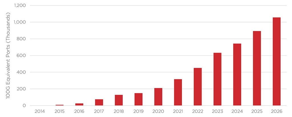
As edge data centers become more common, the issue of interconnecting them becomes more prominent. This situation motivated the Optical Internetworking Forum (OIF) to create the 400ZR and ZR+ standards for pluggable modules. With small enough modules to pack a router faceplate densely, the datacom sector could profit from a 400ZR solution for high-capacity data center interconnects of up to 80km. Cignal AI forecasts that 400ZR shipments will dominate the edge applications, as shown in the figure below.

The 400ZR standard has made coherent technology and dense wavelength division multiplexing (DWDM) the dominant solution in the metro data center interconnects (DCIs) space. Datacom provider operations teams found the simplicity of coherent pluggables very attractive. There was no need to install and maintain additional amplifiers and compensators as in direct detect technology. A single coherent transceiver plugged into a router could fulfill the requirements.
However, there are still obstacles that prevent coherent from becoming dominant in shorter-reach DCI links at the campus (< 10km distance) and intra-datacenter (< 2km distance) level. These spaces require more optical links and transceivers, and coherent technology is still considered too power-hungry and expensive to become the de-facto solution here.
Fortunately, there are avenues for coherent technology to overcome these barriers. By embracing multi-laser arrays, DSP co-design, and electronic ecosystems, coherent technology can mature and become a viable solution for every data center interconnect scenario.
The Promise of Multi-Laser Arrays
Earlier this year, Intel Labs demonstrated an eight-wavelength laser array fully integrated on a silicon wafer. These milestones are essential for optical transceivers because the laser arrays can allow for multi-channel transceivers that are more cost-effective when scaling up to higher speeds.
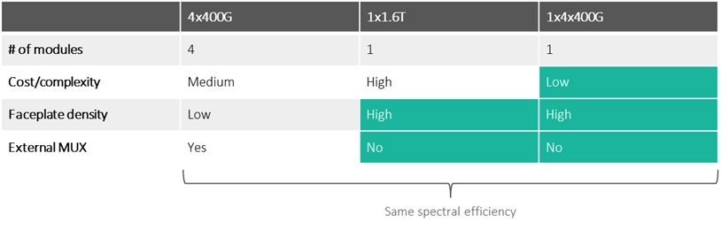
Let’s say we need an intra-DCI link with 1.6 Terabits/s of capacity. There are three ways we could implement it:
- Four modules of 400G: This solution uses existing off-the-shelf modules but has the largest footprint. It requires four slots in the router faceplate and an external multiplexer to merge these into a single 1.6T channel.
- One module of 1.6T: This solution will not require the external multiplexer and occupies just one plug slot on the router faceplate. However, making a single-channel 1.6T device has the highest complexity and cost.
- One module with four internal channels of 400G: A module with an array of four lasers (and thus four different 400G channels) will only require one plug slot on the faceplate while avoiding the complexity and cost of the single-channel 1.6T approach.

Multi-laser array and multi-channel solutions will become increasingly necessary to increase link capacity in coherent systems. They will not need more slots in the router faceplate while simultaneously avoiding the higher cost and complexity of increasing the speed with just a single channel.
Co-designing DSP and Optical Engine for Efficiency and Performance
Transceiver developers often source their DSP, laser, and optical engine from different suppliers, so all these chips are designed separately from each other. This setup reduces the time to market and simplifies the research and design processes but comes with trade-offs in performance and power consumption.
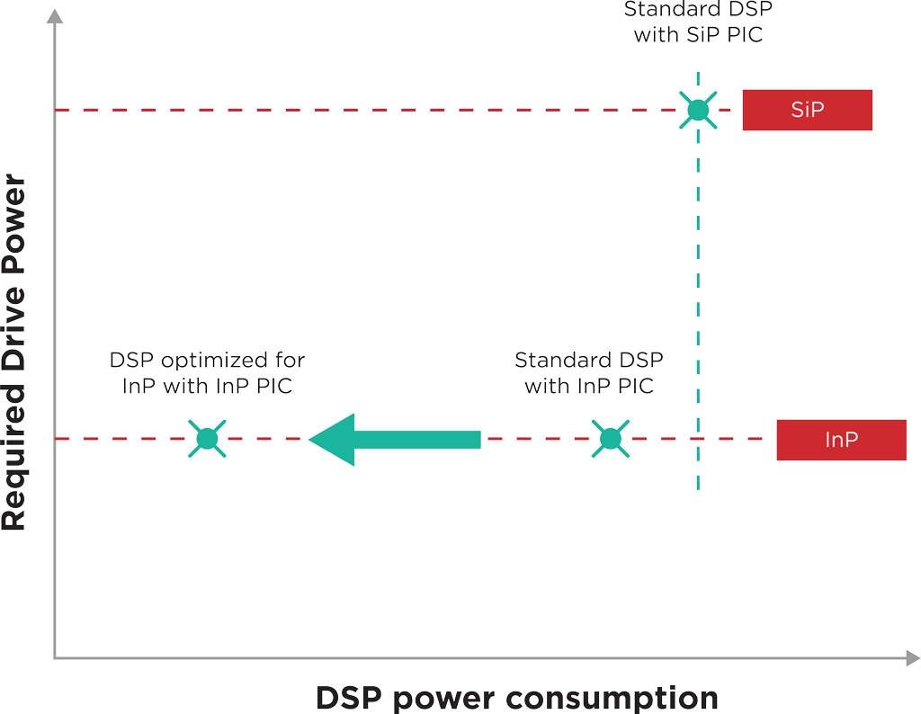
In such cases, the DSP is like a Swiss army knife: a jack of all trades designed for different kinds of optical engines but a master of none. For example, current DSPs are designed to be agnostic to the material platform of the photonic integrated circuit (PIC) they are connected to, which can be Indium Phosphide (InP) or Silicon. Thus, they do not exploit the intrinsic advantages of these material platforms. Co-designing the DSP chip alongside the PIC can lead to a much better fit between these components.
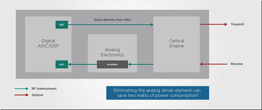
To illustrate the impact of co-designing PIC and DSP, let’s look at an example. A PIC and a standard platform-agnostic DSP typically operate with signals of differing intensities, so they need some RF analog electronic components to “talk” to each other. This signal power conversion overhead constitutes roughly 2-3 Watts or about 10-15% of transceiver power consumption.

However, the modulator of an InP PIC can run at a lower voltage than a silicon modulator. If this InP PIC and the DSP are designed and optimized together instead of using a standard DSP, the PIC could be designed to run at a voltage compatible with the DSP’s signal output. This way, the optimized DSP could drive the PIC directly without needing the RF analog driver, doing away with most of the power conversion overhead we discussed previously.

Additionally, the optimized DSP could also be programmed to do some additional signal conditioning that minimizes the nonlinear optical effects of the InP material, which can reduce noise and improve performance.
Driving Scale Through Existing Electronic Ecosystems
Making coherent optical transceivers more affordable is a matter of volume production. As discussed in a previous article, if PIC production volumes can increase from a few thousand chips per year to a few million, the price per optical chip can decrease from thousands of Euros to mere tens of Euros. Achieving this production goal requires photonics manufacturing chains to learn from electronics and leverage existing electronics manufacturing processes and ecosystems.
While vertically-integrated PIC development has its strengths, a fabless model in which developers outsource their PIC manufacturing to a large-scale foundry is the simplest way to scale to production volumes of millions of units. Fabless PIC developers can remain flexible and lean, relying on trusted large-scale manufacturing partners to guarantee a secure and high-volume supply of chips. Furthermore, the fabless model allows photonics developers to concentrate their R&D resources on their end market and designs instead of costly fabrication facilities.
Further progress must also be made in the packaging, assembly, and testing of photonic chips. While these processes are only a small part of the cost of electronic systems, the reverse happens with photonics. To become more accessible and affordable, the photonics manufacturing chain must become more automated and standardized. It must move towards proven and scalable packaging methods that are common in the electronics industry.
If you want to know more about how photonics developers can leverage electronic ecosystems and methods, we recommend you read our in-depth piece on the subject.
Takeaways
Coherent transceivers are already established as the solution for metro Data Center Interconnects (DCIs), but they need to become more affordable and less power-hungry to fit the intra- and campus DCI application cases. Fortunately, there are several avenues for coherent technology to overcome these cost and power consumption barriers.
Multi-laser arrays can avoid the higher cost and complexity of increasing capacity with just a single transceiver channel. Co-designing the optics and electronics can allow the electronic DSP to exploit the intrinsic advantages of specific photonics platforms such as indium phosphide. Finally, leveraging electronic ecosystems and processes is vital to increase the production volumes of coherent transceivers and make them more affordable.
By embracing these pathways to progress, coherent technology can mature and become a viable solution for every data center interconnect scenario.
