The Power of Integrated Photonic LIDAR
Outside of communications applications, photonics can play a major role in sensing and imaging applications. The most well-known of these sensing applications is Light Detection and Ranging (LIDAR), which is the light-based cousin of RADAR systems that use radio waves.
To put it in a simple way: LIDAR involves sending out a pulse of light, receiving it back, and using a computer to study how the environment changes that pulse. It’s a simple but quite powerful concept.

If we send pulses of light to a wall and listen to how long it takes for them to come back, we know how far that wall is. That is the basis of time-of-flight (TOF) LIDAR. If we send a pulse of light with multiple wavelengths to an object, we know where the object is and whether it is moving towards you or away from you. That is next-gen LIDAR, known as FMCW LIDAR. These technologies are already used in self-driving cars to figure out the location and distance of other cars. The following video provides a short explainer of how LIDAR works in self-driving cars.
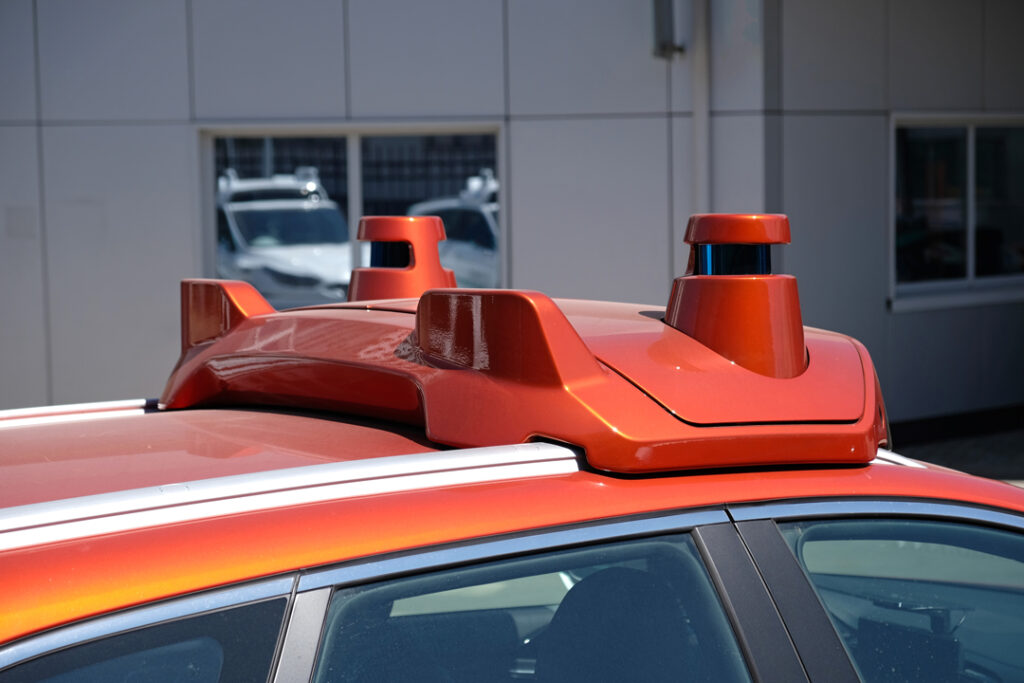
Despite their usefulness, the wider implementation of LIDAR systems is limited by their size, weight, and power (SWAP) requirements. Or, to put it bluntly, they are bulky and expensive. For example, maybe you have seen pictures and videos of self-driving cars with a large LIDAR sensor and scanner on the roof of the car, as in the image below.
Making LIDAR systems more affordable and lighter requires integrating the optical components more tightly and manufacturing them at a higher volume. Unsurprisingly, this sounds like a problem that could be solved by integrated photonics.
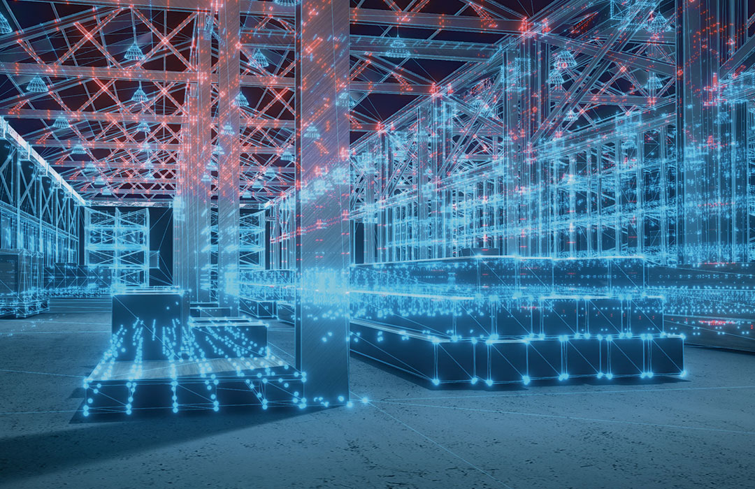
Replacing Bulk LIDAR with “LIDAR on Chip”
Back in 2019, Tesla CEO Elon Musk famously said that “Anyone relying on LIDAR is doomed”. And his scepticism had some substance to it. LIDAR sensors were clunky and expensive, and it wasn’t clear that they would be a better solution than just using regular cameras with huge amounts of visual analysis software. However, the incentive to dominate the future of the automotive sector was too big, and a technology arms race had already begun to miniaturize LIDAR systems into a single photonic chip.
Let’s provide a key example. A typical LIDAR system will require a mechanical system that moves the light source around to scan the environment. This could be as simple as a 360-rotating LIDAR scanner or using small scanning mirrors to steer the beam. However, an even better solution would be to create a LIDAR scanner with no moving parts that could be manufactured at a massive scale on a typical semiconductor process.
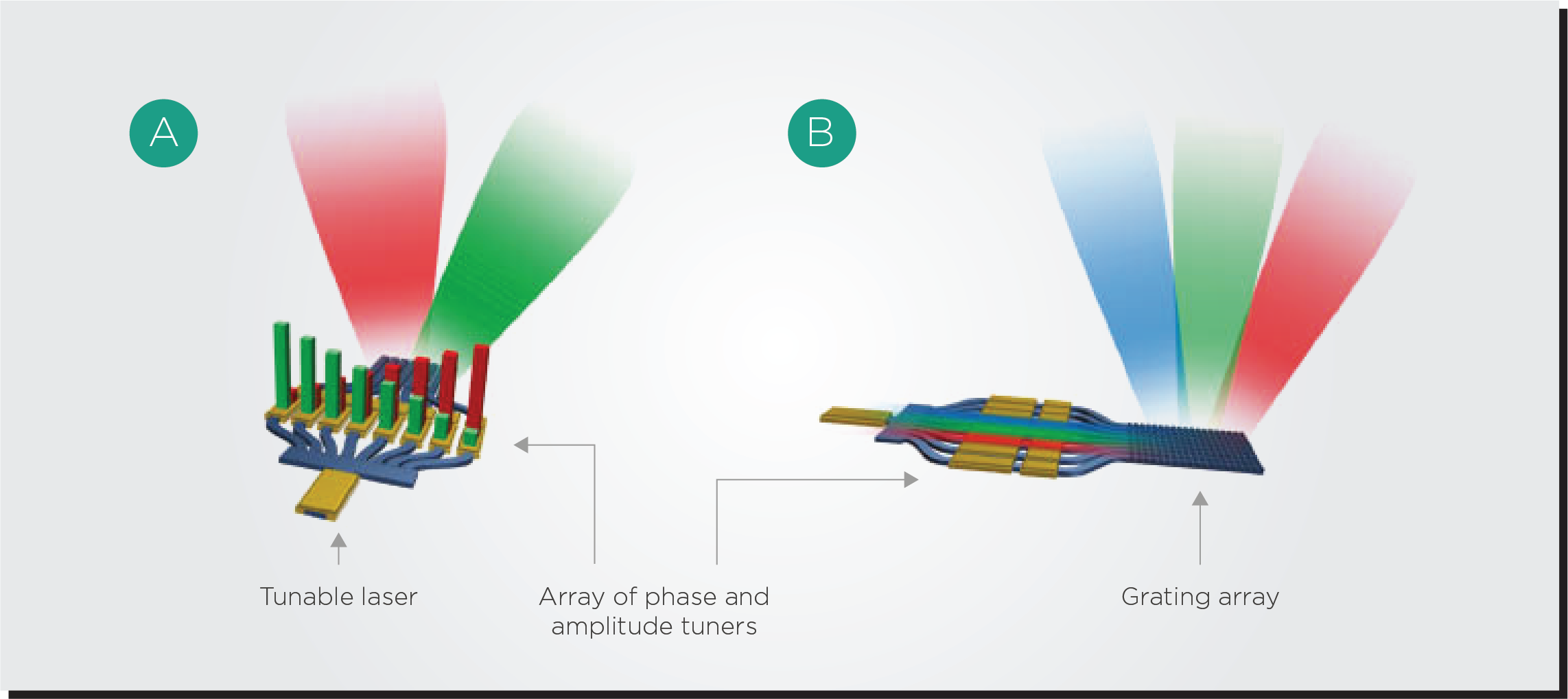
This is where optical phased arrays (OPAs) systems come in. An OPA system splits the output of a tunable laser into multiple channels and puts different time delays on each channels. The OPA will then recombine the channels, and depending on the time delays assigned, the resulting light beam will come out at a different angle. In other words, an OPA system can steer a beam of light from a semiconductor chip without any moving parts.
There is still plenty of development required to bring OPAs into maturity. Victor Dolores Calzadilla, a researcher from the Eindhoven University of Technology (TU/e) explains that “The OPA is the biggest bottleneck for achieving a truly solid-state, monolithic lidar. Many lidar building blocks, such as photodetectors and optical amplifiers, were developed years ago for other applications, like telecommunication. Even though they’re generally not yet optimized for lidar, they are available in principle. OPAs were not needed in telecom, so work on them started much later. This component is the least mature.”
Economics of Scale in LIDAR Systems
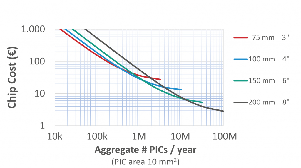
Wafer scale photonics manufacturing demands a higher upfront investment, but the resulting high-volume production line drives down the cost per device. This economy-of-scale principle is the same one behind electronics manufacturing, and the same must be applied to photonics. The more optical components we can integrate into a single chip, the more can the price of each component decrease. The more optical System-on-Chip (SoC) devices can go into a single wafer, the more can the price of each SoC decrease.
Researchers at the Technical University of Eindhoven and the JePPIX consortium have done some modelling to show how this economy of scale principle would apply to photonics. If production volumes can increase from a few thousands of chips per year to a few millions, the price per optical chip can decrease from thousands of Euros to mere tens of Euros. This must be the goal for LIDAR and automotive industry.
By integrating all optical components on a single chip, we also shift the complexity from the assembly process to the much more efficient and scalable semiconductor wafer process. Assembling and packaging a device by interconnecting multiple photonic chips increases assembly complexity and costs. On the other hand, combining and aligning optical components on a wafer at a high volume is much easier, which drives down the device’s cost.
Using Proven Photonics Technologies for Automotive Standards
Another challenge for photonics technologies is that they need to move from into parameters and specifications in the automotive sector that are often harsher than the telecom/datacom sector. For example, a target temperature range of −40°C to 125°C is often required, which is much broader than the typical industrial temperature range used in the telecom sector. The packaging of the PIC and its coupling to fiber and free space is particularly sensitive to these temperature changes.
| Temperature Standard | Temperature Range (°C) | |
| Min | Max | |
| Commercial (C-temp) | 0 | 70 |
| Extended (E-temp) | -20 | 85 |
| Industrial (I-temp) | -40 | 85 |
| Automotive / Full Military | -40 | 125 |
Fortunately, a substantial body of knowledge already exists to make integrated photonics compatible with harsh environments like those of outer space. After all, photonic integrated circuits (PICs) use similar materials to their electronic counterparts, which have already been qualified for space and automotive applications. Commercial solutions, such as those offered by PHIX Photonics Assembly, Technobis IPS, and the PIXAPP Photonic Packaging Pilot Line, are now available.
Takeaways
Photonics technology must be built on a wafer-scale process that can produce millions of chips in a month. When we can show the market that photonics can be as easy to use as electronics, that will trigger a revolution in the use of photonics worldwide.
The broader availability of photonic devices will take photonics into new applications, such as those of LIDAR and the automotive sector. With a growing integrated photonics industry, LIDAR can become lighter, avoid moving parts, and be manufactured in much larger volumes that reduce the cost of LIDAR devices. Integrated photonics is the avenue for LIDAR to become more accessible to everyone.